

Page 1
1
LTC4001
4001f
■
Handheld Battery-Powered Devices
■
Handheld Computers
■
Charging Docks and Cradles
■
Digital Cameras
■
Smart Phones
2A Single Cell Li-Ion Battery Charger
2A Synchronous
Buck Li-Ion Charger
■
Low Power Dissipation
■
2A Maximum Charge Current
■
No External MOSFETs, Sense Resistor or Blocking
Diode Required
■
Remote Sensing at Battery Terminals
■
Programmable Charge Termination Timer
■
Preset 4.2V Float Voltage with ±0.5% Accuracy
■
Programmable Charge Current Detection/Termination
■
Automatic Recharge
■
Thermistor Input for Temperature Qualified Charging
■
Compatible with Current Limited Wall Adapters
■
Low Profile 16-Lead (4mm × 4mm) QFN Package
Power Loss vs V
BAT
Charging (PWM Mode)
FEATURES
DESCRIPTIO
U
APPLICATIO S
U
TYPICAL APPLICATIO
U
The LTC®4001 is a 2A Li-Ion battery charger intended for
5V wall adapters. It utilizes a 1.5MHz synchronous buck
converter topology to reduce power dissipation during
charging. Low power dissipation, an internal MOSFET and
sense resistor allow a physically small charger that can be
embedded in a wide range of handheld applications. The
LTC4001 includes complete charge termination circuitry,
automatic recharge and a ±1% 4.2V float voltage. Input
short-circuit protection is included so no blocking diode is
required.
Battery charge current, charge timeout and end-of-charge
indication parameters are set with external components.
Additional features include shorted cell detection, temperature qualified charging and overvoltage protection. The
LTC4001 is available in a low profile (0.75mm) 16-lead
(4mm × 4mm) QFN package.
, LT, LTC and LTM are registered trademarks of Linear Technology Corporation.
All other trademarks are the property of their respective owners.
+
PROG
EN
FAULT
NTC
CHRG
PGND
PV
IN
V
INSENSE
BAT
BATSENS
IDET TIMER
274Ω
0.22µF
10µF
4001 TA01a
4.2V
Li-Ion
10µF
V
IN
4.5V TO 5.5V
0.1µF
SS
SW SENSE
LTC4001
1.5µH
GNDSENS
V
BAT
(V)
3
TOTAL APPLICATION CIRCUIT POWER
DISSIPATION (W)
0.75
1.00
1.25
4
4001 TA01b
0.50
0.25
0
3.25
3.5
3.75
4.25
VIN = 5V
2A CHARGER
Page 2
2
LTC4001
4001f
Consult LTC Marketing for parts specified with wider operating temperature ranges.
ABSOLUTE AXI U RATI GS
WWWU
PACKAGE/ORDER I FOR ATIO
UU
W
(Note 1)
LTC4001EUF
ORDER PART NUMBER UF PART MARKING
4001
T
JMAX
= 125°C, θJA = 37°C/W
EXPOSED PAD (PIN 17) IS GND, MUST BE SOLDERED TO PCB
16 15 14 13
5 6 7 8
TOP VIEW
17
UF PACKAGE
16-LEAD (4mm × 4mm) PLASTIC QFN
9
10
11
12
4
3
2
1BAT
SENSE
PGND
GNDSENS
PROG
NTC
FAULT
V
INSENSE
BATSENS
TIMERSSIDET
SW
EN
CHRG
PV
IN
SYMBOL PARAMETER CONDITIONS MIN TYP MAX UNITS
V
IN
Supply Voltage (Note 2) 4 5.5 V
I
IN
PVIN Connected to V
INSENSE
, PROG and IDET 2 mA
Pins Open, Charger On
Shutdown, EN = V
IN
50 µA
V
FLOATVBAT
Regulated Float Voltage Measured from BATSENS to GNDSENS
●
4.158 4.2 4.242 V
4.179 4.2 4.221 V
I
BAT
Current Mode Charge Current R
PROG
= 549Ω, V
BAT
= 3.5V 1.8 2 2.2 A
R
PROG
= 1.10k, V
BAT
= 3.5V 0.9 1 1.1 A
Shutdown, EN = V
IN
±5 µA
I
TRIKL
Trickle Charge Current V
BAT
= 2V 35 50 65 mA
V
TRIKL
Trickle Charge Threshold V
BAT
Rising 3.05 3.1 3.20 V
V
BAT
Falling 2.85 3.0 3.05 V
V
UVL
VIN Undervoltage Lockout Voltage VIN Rising, Measured from V
INSENSE
to GNDSENS 2.7 2.82 V
∆V
UVL
VIN Undervoltage Lockout Hysteresis Measured from V
INSENSE
to GNDSENS 100 mV
V
ASD
Automatic Shutdown Threshold V
INSENSE
– V
BATSENS
Rising (Turn-On), V
BATSENSE
= 4V 200 250 300 mV
Voltage V
INSENSE
– V
BATSENS
Falling (Turn-Off), V
BATSENSE
= 4V 15 30 60 mV
f
OSC
Oscillator Frequency 1.3 1.5 1.7 MHz
D Maximum Duty Factor 100 %
R
PFET
R
DS(ON)
of P-Channel MOSFET Measured from PVIN to SW 127 mΩ
R
NFET
R
DS(ON)
of N-Channel MOSFET Measured from SW to PGND 121 mΩ
The ● denotes specifications which apply over the full operating temperature range, otherwise specifications are TA = 25°C.
V
IN
= 5V, VEN = 0V, R
PROG
= 549Ω, R
IDET
= 549Ω, unless otherwise specified.
ELECTRICAL CHARACTERISTICS
Order Options Tape and Reel: Add #TR
Lead Free: Add #PBF Lead Free Tape and Reel: Add #TRPBF
Lead Free Part Marking: http://www.linear.com/leadfree/
PVIN, V
INSENSE
t < 1ms, DC < 1% .................................... –0.3V to 7V
Steady State ............................................ –0.3V to 6V
SW, SENSE, BAT, BATSENS, SS, FAULT, CHRG, EN,
NTC, PROG, IDET, TIMER Voltage .............. – 0.3V to 6V
Operating Temperature Range (Note 3) .. –40°C to 85°C
Operating Junction Temperature
(Note 5) ............................................... – 40°C to 125°C
Storage Temperature Range ................ –65°C to 125°C
Page 3
3
LTC4001
4001f
SYMBOL PARAMETER CONDITIONS MIN TYP MAX UNITS
t
TIMER
Timer Accuracy C
TIMER
= 0.22µF ±10 %
V
EN
Enable Input Threshold Voltage VEN Rising 0.6 0.8 1 V
∆V
EN
Enable Input Hysteresis 100 mV
V
PROG
PROG Pin Voltage R
PROG
= 549Ω 1.213 V
V
IDET
IDET Pin Voltage R
IDET
= 549Ω 1.213 V
I
IDET
IDET Threshold R
IDET
= 549Ω 150 200 250 mA
I
CHRG
CHRG Pin Weak Pull-Down Current V
CHRG
= 1V 15 30 50 µA
V
CHRG
CHRG Pin Output Low Voltage I
CHRG
= 5mA 0.2 0.4 V
V
OL
FAULT Pin Output Low Voltage 1mA Load 0.4 V
V
OH
FAULT Pin Output High Voltage 1mA Load 4.6 V
V
RECHRG
Recharge Battery Threshold Voltage V
FLOAT
– V
RECHRG VBAT
Falling 50 100 135 mV
t
RB
Recharge Filter Time Constant 4 ms
t
RECHRG
Recharge Time Percent of Total Charge Time 50 %
t
TRIKL
Low-Battery Trickle Charge Time Percent of Total Charge Time, V
BAT
< 2.8V, 25 %
Measured Using BATSENS and GNDSENS Pins
I
SS
Soft-Start Ramp Current V
BAT
< V
FLOAT
– 100mV, V
BAT
Across BATSENS 6 12.8 16 µA
and GNDSENS Pins
V
COLD
NTC Pin Cold Temperature Fault From NTC to GNDSENS Pin
Threshold Rising Threshold 0.74 V
INSENSE
V
Falling Threshold 0.72 V
INSENSE
V
V
HOT
NTC Pin Hot Temperature Fault From NTC to GNDSENS Pin
Threshold Falling Threshold 0.29 V
INSENSE
V
Rising Threshold 0.30 V
INSENSE
V
V
DIS
NTC Disable Threshold (Falling) From NTC to GNDSENS Pin 0.015 • 0.02 • 0.025 • V
V
INSENSEVINSENSEVINSENSE
∆V
DIS
NTC Disable Hysteresis From NTC to GNDSENS Pin 0.01 • V
INSENSE
V
The ● denotes specifications which apply over the full operating temperature range, otherwise specifications are TA = 25°C.
V
IN
= 5V, VEN = 0V, R
PROG
= 549Ω, R
IDET
= 549Ω, unless otherwise specified.
ELECTRICAL CHARACTERISTICS
Note 1: Stresses beyond those listed under Absolute Maximum Ratings
may cause permanent damage to the device. Exposure to any Absolute
Maximum Rating condition for extended periods may affect device
reliability and lifetime.
Note 2: Operation with current limited wall adapters is allowed down to the
undervoltage lockout threshold.
Note 3: The LTC4001E is guaranteed to meet performance specifications
from 0°C to 85°C. Specifications over the –40°C to 85°C operating
temperature range are assured by design, characterization and correlation
with statistical process controls.
Note 4: T
J
is calculated from the ambient temperature TA and power
dissipation P
D
according to the following formula:
T
J
= TA + (PD • 37°C/W)
Note 5: This IC includes overtemperature protection that is intended to
protect the device during momentary overload. Junction temperature will
exceed 125°C when overtemperature protection is active. Continuous
operation above the specified maximum operating junction temperature
my impair device reliability.
Page 4
4
LTC4001
4001f
TYPICAL PERFOR A CE CHARACTERISTICS
UW
Oscillator Frequency vs V
IN
Oscillator Frequency
vs Temperature
Dissipation of Figure 8 Circuit
vs I
BAT
PROG Pin Characteristic
(V
PROG
vs I
PROG
)
Dissipation of Figure 8 Circuit
vs V
IN
Trickle Charge Current vs V
BAT
V
FLOAT
and Recharge Battery
Threshold Voltage vs Temperature
Output Charging Characteristic
Showing Constant Current and
Constant Voltage Operation
(T
A
= 25°C unless otherwise noted)
VIN (V)
3
PERCENT VARIATION (%)
–0.25
0
0.25
4.5
5.5
4001 G01
–0.50
–0.75
–1.00
3.5 4 5
0.50
0.75
1.00
6
V
BAT
= 3.2V
V
SS
= 1V
I
PROG
(mA)
0
0.8
1.0
15
4001 G05
0.6
0.4
510 20
0.2
0
1.2
V
PROG
(V)
VIN = 5V
V
BAT
= 3.2V V
BAT
= 4V
V
BAT
= 3.5V
V
BAT
= 3.7V
V
BAT
(V)
0
0
I
BAT
(A)
0.5
1.0
1.5
2.0
0.5 1 1.5 2
4001 G06
2.5 3 3.5 4
V
BAT
(V)
0
40
I
BAT
(mA)
45
50
55
0.5 1 1.5 2
4001 G07
2.5 3
VIN = 5.5V
VIN = 5V
VIN = 4V
VIN = 4.5V
TEMPERATURE (°C)
–50
FREQUENCY VARIATION FROM 25°C (%)
0.4
0.6
0.8
110
4001 G02
0.2
0
–0.2
–30 –10 10
30 50
70 90 130
150
VIN = 5V
V
BAT
= 3.2V
V
SS
= 1V
I
BAT
(mA)
500
TOTAL APPLICATION CIRCUIT POWER
DISSIPATION (W)
0.50
0.75
4001 G03
0.25
0
1000
1500
2000
1.25
1.00
V
IN
= 5V
V
BAT
= 4V
VIN (V)
4.25
1.0
1.2
1.4
5.25
4001 G04
0.8
0.6
4.5 4.75 5 5.5
0.4
0.2
0
TOTAL APPLICATION CIRCUIT POWER
DISSIPATION (W)
I
BAT
= 2A
V
BAT
= 4V
I
BAT
= 1.5A
I
BAT
= 1A
I
BAT
= 500mA
TEMPERATURE (°C)
4.0
FLOAT AND RECHARGE VOLTAGES (V)
4.1
4.2
4.3
–10 30 70 110
4001 G08
150–30–50 10 50 90 130
V
FLOAT
V
RECHARGE
(V
BAT
FALLING)
Page 5
5
LTC4001
4001f
TYPICAL PERFOR A CE CHARACTERISTICS
UW
Soft-Start (PWM Mode)
IDET Threshold vs R
IDET
for
R
PROG
= 549Ω
UU
U
PI FU CTIO S
BAT (Pin 1): Battery Charger Output Terminal. Connect a
10µF ceramic chip capacitor between BAT and PGND to
keep the ripple voltage small.
SENSE (Pin 2): Internal Sense Resistor. Connect to external inductor.
PGND (Pin 3): Power Ground.
GNDSENS (Pin 4): Ground Sense. Connect this pin to the
negative battery terminal. GNDSENS provides a Kelvin
connection for PGND and must be connected to PGND
schematically.
SW (Pin 5): Switch Node Connection. This pin connects to
the drains of the internal main and synchronous power
MOSFET switches. Connect to external inductor.
EN (Pin 6): Enable Input Pin. Pulling the EN pin high places
the LTC4001 into a low power state where the BAT drain
current drops to less than 3µA and the supply current is
reduced to less than 50µA. For normal operation, pull the
pin low.
CHRG (Pin 7): Open-Drain Charge Status Output. When
the battery is being charged, CHRG is pulled low by an
internal N-channel MOSFET. When the charge current
drops below the IDET threshold (set by the R
IDET
programming resistor) for more than 5milliseconds, the N-channel
MOSFET turns off and a 30µA current source is connected
from CHRG to ground. (This signal is latched and is reset
by initiating a new charge cycle.) When the timer runs out
or the input supply is removed, the current source will be
disconnected and the CHRG pin is forced to a high impedance state. A temperature fault causes this pin to blink.
PV
IN
(Pin 8): Positive Supply Voltage Input. This pin
connects to the power devices inside the chip. V
IN
ranges
from 4V to 5.5V for normal operation. Operation down to
the undervoltage lockout threshold is allowed with current
limited wall adapters. Decouple with a 10µF or larger
surface mounted ceramic capacitor.
V
INSENSE
(Pin 9): Positive Supply Sense Input. This pin
connects to the inputs of all input comparators (UVL, V
IN
to V
BAT
). It also supplies power to the controller portion of
this chip. When the BATSENS pin rises to within 30mV of
V
INSENSE
, the LTC4001 enters sleep mode, dropping IIN to
50µA. Tie this pin directly to the terminal of the PV
IN
decoupling capacitor.
CHRG Pin Temperature Fault
Behavior (Detail)
0
INPUT
CURRENT (I
IN
)
0.5A/DIV
INDUCTOR
CURRENT (I
L
)
0.5A/DIV
SOFT-START
VOLTAGE (V
SS
)
1V/DIV
EN PIN (V
EN
)
5V/DIV
0
0
0
2ms/DIVV
BAT
= 3.5V
V
IN
= 5V
4001 G09
R
IDET
(Ω)
300
IDET (mA)
200
250
300
1100
4001 G10
150
100
0
500
700
900
400 1200
600
800
1000
50
400
350
CHRG
1V/DIV
TIME (20µs/DIV)
4001 G11
Page 6

6
LTC4001
4001f
FAULT (Pin 10): Battery Fault. This pin is a logic high if a
shorted battery is detected or if a temperature fault is
detected. A temperature fault occurs with the temperature
monitor circuit enabled and the thermistor temperature is
either below 0°C or above 50°C (typical).
NTC (Pin 11): Input to the NTC (Negative Temperature
Coefficient) Thermistor Temperature Monitoring Circuit.
Under normal operation, tie a thermistor from the NTC pin
to the GNDSENS pin and a resistor of equal value from NTC
to VIN. When the voltage on this pin is above 0.74VIN (Cold,
0°C) or below 0.29V
IN
(Hot, 50°C), charging is disabled
and the CHRG pin blinks. When the voltage on NTC comes
back between 0.74V
IN
and 0.29VIN, the timer continues
where it left off and charging resumes. There is approximately 3°C of temperature hysteresis associated with
each of the input comparators. If the NTC function is not
used connect the NTC pin to GNDSENS. This will disable
all of the NTC functions. NTC should never be pulled above
VIN.
PROG (Pin 12): Charge Current Program. The R
PROG
resistor connects from this pin to GNDSENS, setting the
current:
R
k
I
PROG
BAT AMPS
=
1 110.
()
where I
BAT
is the high rate battery charging current.
UU
U
PI FU CTIO S
IDET (Pin 13): Charge Rate Detection Threshold. Connecting a resistor, R
IDET
to GNDSENS programs the charge
rate detection threshold. If R
IDET
= R
PROG
, CHRG provides
an I
BAT
/10 indication. For other thresholds see the Appli-
cations Information section.
SS (Pin 14): Soft-Start/Compensation. Provides soft-start
function and compensation for the float voltage control
loop and compensation for the charge current control
loop. Tie a soft-start/compensation capacitor between this
pin and GNDSENS.
TIMER (Pin 15): Timer Capacitor. The timer period is set
by placing a capacitor, C
TIMER
, to GNDSENS. Set C
TIMER
to:
C
TIMER
= Time (Hrs) • 0.0733 (µF)
where time is the desired charging time.
Connect this pin to IDET to disable the timer. Connect this
pin to GNDSENS to end battery charging when I
BAT
drops
below the IDET charge rate threshold.
BATSENS (Pin 16): Battery Sense Input. An internal resistor divider sets the final float voltage at this pin. The
resistor divider is disconnected in sleep mode or when
EN = H to reduce the battery drain current. Connect this pin
to the positive battery terminal.
Exposed Pad (Pin 17): Ground. This pin must be soldered
to the PCB ground (PGND) for electrical contact and rated
thermal performance.
Page 7
7
LTC4001
4001f
BLOCK DIAGRA
W
BATTERY
OVERVOLTAGE
COMPARATOR
VOLTAGE
REFERENCE
+
–
UNDERVOLTAGE
COMPARATOR
FLOAT VOLTAGE
ERROR AMP
RECHARGE
COMPARATOR
LOW-BATTERY
COMPARATOR
SHUTDOWN
COMPARATOR
OVERCURRENT
COMPARATOR
CURRENT
REVERSAL
COMPARATOR
+
–
+
–
CHARGE CURRENT
ERROR AMP
PROG
ERROR
AMP
PROG SHORT
COMPARATOR
+
–
IDET
COMPARATOR
+
–
1.2V
150mV
GNDSENS
4001 BD
+
–
+
–
SOFT-START
COPMPARATOR
+
–
1.1V
1.2V
LOW CURRENT
V
IN
GOOD
RECHARGE
DISCHARGE SS
PROG SHORTED
SS LOW
OVERVOLTAGE
CHIP OVER TEMP
CHIP
OVERTEMP
COMPARATOR
CONNECT
PWM ON
TRICKLE ON
OVERCURRENT
SHUTDOWN
LOW BATTERY
+
–
+
–
+
–
4
PROGIDET
12
13
GND
17
50mA
BAT
9
V
INSENSE
16
BATSENSSENSE
2
SW
5
+
–
1
+
–
+
–
PGND
DRIVER
PWM
COMPARATOR
OSCILLATOR
Q
S
SS
RD
3
PV
IN
8
11
CLK
RAMP
+
–
TFAULT
NTC
NTC
COMPARATOR
15
TIMER
TIMER
10
FAULT
LOGIC
FAULT
7
CHRG
CHRG
6
EN
EN
14
SS
Page 8

8
LTC4001
4001f
OPERATIO
U
The LTC4001 is a constant current, constant voltage
Li-Ion battery charger based on a synchronous buck
architecture. Low power dissipation makes continuous
high rate (2A) battery charging practical. The battery DC
charge current is programmed by a resistor R
PROG
(or a
DAC output current) at the PROG pin. The final battery float
voltage is internally set to 4.2V.
Charging begins when the VIN voltage rises above the
UVLO level (approximately 2.75V), V
IN
is 250mV greater
than the battery voltage and EN is low. At the beginning of
the charge cycle, if the battery voltage is less than the
trickle charge threshold, 3V, the charger goes into trickle
charge mode and delivers approximately 50mA to the
battery using a linear charger. If the battery voltage stays
low for more than one quarter of the charge time, the
battery is considered faulty, the charge cycle is terminated
and the FAULT pin produces a logic high output.
When the battery voltage exceeds the trickle charge threshold, the low rate linear charger is turned off and the high
rate PWM charger ramps up (based on the SS pin capacitance) reaching its full-scale constant current (set via the
PROG pin). When the battery approaches the float voltage,
the charge current will start to decrease. When the charge
current drops below the charge rate detection threshold
(set via the IDET pin) for more than 5ms, an internal
comparator turns off the internal pull-down N-channel
MOSFET at the CHRG pin, and connects a weak current
source (30µA typical) to ground to indicate a near end-of-
charge condition.
Total charge time is set by an external capacitor connected
to the timer pin. After timeout occurs, the charge cycle is
terminated and the CHRG pin is forced to a high impedance state. To restart the charge cycle, remove and reapply
the input voltage, or momentarily shut the charger down
via the EN pin. Also, a new charge cycle will begin if the
battery voltage drops below the recharge threshold voltage (100mV below the float voltage). A recharge cycle
lasts only one-half of the normal charge time.
A negative temperature coefficient (NTC) thermistor located close to the battery pack can be used to monitor
battery temperature and suspend charging when battery
temperature is outside the 0°C to 50°C window. A temperature fault drives the FAULT pin high and makes the
CHRG pin blink. When the input voltage (V
IN
) is present,
the charger can be shut down by pulling the EN pin up.
IDET Blanking
The IDET comparator provides an end-of-charge indication by sensing when battery charge current is less than
the IDET threshold. To prevent a false end-of-charge
indication from occurring during soft-start, this comparator is blanked until the battery voltage approaches the float
voltage.
Automatic Battery Recharge
After the charge cycle is completed and if both the battery
and the input power supply (wall adapter) are still connected, a new charge cycle will begin if the battery voltage
drops below 4.1V due to self-discharge or external loading. This will keep the battery near maximum capacity at all
times without manually restarting the charge cycle.
In some applications such as battery charging in GPRS
cellphones, large load current transients may cause battery voltage to momentarily drop below the recharge
threshold. To prevent these transients from initiating a
recharge cycle when it is not needed, the output of the
recharge comparator is digitally qualified. Only if the
battery voltage stays below the recharge threshold for at
least 4ms will battery recharging occur. (GPRS qualification is available even if timeout is disabled.)
Undervoltage Lockout and Automatic Shutdown
Internal undervoltage lockout circuits monitor V
IN
and
keep the charger circuits shut down until V
IN
rises above
the undervoltage lockout threshold (3V). The UVLO has a
built-in hysteresis of 100mV. Furthermore, to protect
against reverse current, the charger also shuts down if V
IN
is less than V
BAT
. If automatic shutdown is tripped, V
IN
must increase to more than 250mV above V
BAT
to allow
charging.
Page 9

9
LTC4001
4001f
OPERATIO
U
Overvoltage, Chip Overtemperature and Short-Circuit
Current Protection
The LTC4001 includes overvoltage, chip overtemperature
and several varieties of short-circuit protection.
A comparator turns off both chargers (high rate and
trickle) if battery voltage exceeds the float voltage by
approximately 5%. This may occur in situations where the
battery is accidentally disconnected while battery charging is underway.
A comparator continuously monitors on-chip temperature
and will shut off the battery charger when chip temperature
exceeds approximately 160°C. Battery charging will be
enabled again when temperature drops to approximately
150°C.
Short-circuit protection is provided in several different
ways. First, a hard short on the battery terminals will
cause the charge to enter trickle charge mode, limiting
charge current to the trickle charge current (typically
50mA). Second, PWM charging is prevented if the high
rate charge current is programmed far above the 2A
maximum recommended charge current (via the PROG
pin). Third, an overcurrent comparator monitors the peak
inductor current.
Page 10
10
LTC4001
4001f
APPLICATIO S I FOR ATIO
WUUU
Soft-Start and Compensation Capacitor Selection
The LTC4001 has a low current trickle charger and a
PWM-based high current charger. Soft-start is used whenever the high rate charger is initially turned on, preventing
high start-up current. Soft-start ramp rate is set by the
internal 12.8µA pull-up current and an external capacitor.
The control range on the SS pin is approximately 0.3V to
1.6V. With a 0.1µF capacitor, the time to ramp up to
maximum duty cycle is approximately 10ms.
The external capacitor on the SS pin also sets the compensation for the current control loop and the float voltage
control loop. A minimum capacitance of 10nF is required.
Charge Current and IDET Programming
The LTC4001 has two different charge modes. If the
battery is severely depleted (battery voltage less than
2.9V) a 50mA trickle current is initially used. If the battery
voltage is greater than the trickle charge threshold, high
rate charging is used.
This higher charge current is programmable and is approximately 915 times the current delivered by the PROG
pin. This current is usually set with an external resistor
from PROG to GNDSENS, but it may also be set with a
current output DAC connected to the PROG pin. The
voltage on the PROG pin is nominally 1.213V.
For 2A charge current:
R
V
A
PROG
= ≅Ω
915 1 213
2
554 9•..
The IDET threshold (a charge current threshold used to
determine when the battery is nearly fully charged) is
programmed in much the same way as the PROG pin,
except that the IDET threshold is 91.5 times the current
delivered by the IDET pin. This current is usually set with
an external resistor from IDET to ground, but it may also
be set with a current output DAC. The voltage on the PROG
pin is nominally 1.213V.
For 200mA IDET current (corresponding to C/10 for a
2AHr battery):
R
V
A
IDET
= ≅Ω
91 5 1 213
02
554 9
.•.
.
.
1.10kΩ programs approximately 100mA and 274Ω approximately 400mA.
For applications where IDET is set to one tenth of the high
rate charge current, and slightly poorer charger current
and IDET threshold accuracy is acceptable, the PROG and
IDET pins may be tied together and a single resistor, R1,
can program both (Figure 1).
R
I
CHARGE
1
457 5 1 213
=
.•.
and
IDET
I
CHARGE
=
10
Figure 1. Programming Charge Current and IDET Threshold
with a Single Resistor
PROG
LTC4001
IDET
R1
274Ω FOR 2A
GNDSENS
4001 F01
Page 11
11
LTC4001
4001f
The equations for calculating R1 (used in single resistor
programming) differ from the equations for calculating
R
PROG
and R
IDET
(2-resistor programming) and reflect the
fact that the current from both the IDET and PROG pins
must flow through a single resistor R1 when a single
programming resistor is used.
CHRG Status Output Pin
When a charge cycle starts, the CHRG pin is pulled to
ground by an internal N-channel MOSFET which is capable
of driving an LED. When the charge current drops below
the end-of-charge (IDET) threshold for at least 4ms, and
the battery voltage is close to the float voltage, the N-channel
MOSFET turns off and a weak 30µA current source to
ground is connected to the CHRG pin. This weak pulldown remains until the charge cycle ends. After charging
ends, the pin will become high impedance. By using two
different value resistors, a microprocessor can detect
three states from this pin (charging, end-of-charge and
charging stopped). See Figure 2.
To detect the charge mode, force the digital output pin,
OUT, high and measure the voltage on the CHRG pin. The
N-channel MOSFET will pull the pin low even with a 2k pullup resistor. Once the charge current drops below the endof-charge threshold, the N-channel MOSFET is turned off
and a 30µA current source is connected to the CHRG pin.
The IN pin will then be pulled high by the 2k resistor
connected to OUT. Now force the OUT pin into a high
impedance state, the current source will pull the pin low
through the 390k resistor. When charging stops, the
CHRG pin changes to a high impedance state and the 390k
resistor will then pull the pin high to indicate charging has
stopped.
Charge Termination
Battery charging may be terminated several different ways,
depending on the connections made to the TIMER pin. For
time-based termination, connect a capacitor between the
TIMER pin and GNDSENS (C
TIMER
= Time(Hrs) 0.0733µF).
Charging may be terminated when charge current drops
below the IDET threshold by tying TIMER to GNDSENS.
Finally, charge termination may be defeated by tying
TIMER to IDET. In this case, an external device can
terminate charging by pulling the EN pin high.
Battery Temperature Detection
When battery temperature is out of range (either too hot or
too cold) charging is temporarily halted and the FAULT pin
is driven high. In addition, if the battery is still charging at
a high rate (greater than the IDET current) when a temperature fault occurs, the CHRG pin NMOS turns on and off
at approximately 50kHz, alternating between a high and
low duty factor at an approximate rate of 1.5Hz (Figure 3).
This provides a low rate visual indication (1.5Hz) when
driving an LED from the CHRG pin while providing a fast
temperature fault indication (20useconds typical) to a
microprocessor by tying the CHRG pin to an interrupt line.
Serrations within this pulse are typically 500ns wide.
APPLICATIO S I FOR ATIO
WUUU
Figure 2. Microprocessor Interface
Figure 3. CHRG Temperature Fault Waveform
LTC4001
V
IN
V
DD
IN
OUT
µPROCESSOR
CHRG
R2
2k
R1
390k
4001 F02
20µs
4001 F03
667ms
Page 12

12
LTC4001
4001f
The battery temperature is measured by placing a negative
temperature coefficient (NTC) thermistor close to the
battery pack. To use this feature, connect the NTC thermistor, R
NTC
, between the NTC pin and GNDSENS and the
resistor, R
NOM
, from the NTC pin to V
INSENSE
. R
NOM
should be a 1% resistor with a value equal to the value of
the chosen NTC thermistor at 25°C. The LTC4001 goes
into hold mode when the resistance, R
HOT
, of the NTC
thermistor drops to 0.41 times the value of R
NOM
. For
instance for R
NTC
= 10k. (The value for a Vishay
NTHS0603N02N1002J thermistor at 25°C) hold occurs at
approximately 4.1k, which occurs at 50°C. The hold mode
freezes the timer and stops the charge cycle until the
thermistor indicates a return to a valid temperature. As the
temperature drops, the resistance of the NTC thermistor
rises. The LTC4001 is designed to go into hold mode when
the value of the NTC thermistor increases to 2.82 times the
value of R
NOM
. This resistance is R
COLD
. For the Vishay 10k
thermistor, this value is 28.2k, which corresponds to
approximately 0°C. The hot and cold comparators each
have approximately 3°C of hysteresis to prevent oscillation about the trip point. Grounding the NTC pin disables
the NTC function.
Thermistors
The LTC4001 NTC trip points were designed to work with
thermistors whose resistance temperature characteristics
follow Vishay Dale’s “R-T Curve 2.” However, any thermistor whose ratio of R
COLD
to R
HOT
is about 7 will also
work (Vishay Dale R-T Curve 2 shows a ratio of R
COLD
to
R
HOT
of 2.815/0.4086 = 6.89).
Power conscious designs may want to use thermistors
whose room temperature value is greater than 10k. Vishay
Dale has a number of values of thermistor from 10k to
100k that follow the “R-T Curve 1.” Using these as indicated in the NTC Thermistor section will give temperature
trip points of approximately 3°C and 47°C, a delta of 44°C.
This delta in temperature can be moved in either direction
by changing the value of R
NOM
with respect to R
NTC
.
Increasing R
NOM
will move the trip points to higher tem-
peratures. To calculate R
NOM
for a shift to lower tempera-
ture for example, use the following equation:
R
R
RatC
NOM
COLD
NTC
=°
2 81525.
•
where R
COLD
is the resistance ratio of R
NTC
at the desired
cold temperature trip point. If you want to shift the trip
points to higher temperatures use the following equation:
R
R
RatC
NOM
HOT
NTC
=°
0 4086
25
.
•
where R
HOT
is the resistance ratio of R
NTC
at the desired
hot temperature trip point.
Here is an example using a 100k R-T Curve 1 thermistor
from Vishay Dale. The difference between trip points is
44°C, from before, and we want the cold trip point to be
0°C, which would put the hot trip point at 44°C. The R
NOM
needed is calculated as follows:
R
R
RatC
kk
NOM
COLD
NTC
=°
==
2 815
25
3 266
2 815
100 116
.
•
.
.
•
The nearest 1% value for R
NOM
is 115k. This is the value
used to bias the NTC thermistor to get cold and hot trip
points of approximately 0°C and 44°C respectively. To
extend the delta between the cold and hot trip points a
resistor, R1, can be added in series with R
NTC
(see
Figure 4). The values of the resistors are calculated as
follows:
R
RR
RRRR
NOM
COLD HOT
COLD HOT HOT
=
=
()
–
.–.
.
.–.
•––
2 815 0 4086
1
0 4086
2 815 0 4086
APPLICATIO S I FOR ATIO
WUUU
Page 13
13
LTC4001
4001f
where R
NOM
is the value of the bias resistor, R
HOT
and
R
COLD
are the values of R
NTC
at the desired temperature
trip points. Continuing the example from before with a
desired hot trip point of 50°C:
R
RR
k
k k is nearest
Rk
k k is nearest
NOM
COLD HOT
==
()
=
=
()
⎛
⎝
⎜
⎞
⎠
⎟
=
–
.–.
•. –.
.–.
., %
•
.
.–.
• . –. –.
., . %
2 815 0 4086
100 3 2636 0 3602
2 815 0 4086
120 8 121 1
1 100
0 4086
2 815 0 4086
3 266 0 3602 0 3602
13 3 13 3 1
The final solution is as shown if Figure 4 where R
NOM
=
121k, R1 = 13.3k and R
NTC
= 100k at 25°C.
Input and Output Capacitors
The LTC4001 uses a synchronous buck regulator to provide high battery charging current. A 10µF chip ceramic
APPLICATIO S I FOR ATIO
WUUU
capacitor is recommended for both the input and output
capacitors because it provides low ESR and ESL and can
handle the high RMS ripple currents. However, some high
Q capacitors may produce high transients due to selfresonance under some start-up conditions, such as connecting the charger input to a hot power source. For more
information, refer to Application Note 88.
EMI considerations usually make it desirable to minimize
ripple current in the battery leads, and beads or inductors
may be added to increase battery impedance at the 1.5MHz
switching frequency. Switching ripple current splits between the battery and the output capacitor depending on
the ESR of the output capacitor and the battery impedance.
If the ESR of the output capacitor is 0.1Ω and the battery
impedance is raised to 2Ω with a bead or inductor, only 5%
of the ripple current will flow in the battery. Similar
techniques may also be applied to minimize EMI from the
input leads.
Figure 4. Extending the Delta Temperature
TOO COLD
LTC4001 NTC BLOCK
TOO HOT
0.29 • V
INSENSE
0.74 • V
INSENSE
R
NOM
121k
V
INSENSE
0.02 • V
INSENSE
NTC ENABLE
4001 F04
–
+
–
+
–
+
R1
13.3k
R
NTC
100k
9
NTC
11
GNDSENS
4
Page 14

14
LTC4001
4001f
Inductor Selection
A high (1.5MHz) operating frequency was chosen for the
buck switcher in order to minimize the size of the inductor.
However, take care to use inductors with low core losses
at this frequency. A good choice is the IHLP-2525AH-01
from Vishay Dale.
To calculate the inductor ripple current:
∆ =I
V
V
V
Lf
L
BAT
BAT
IN
–
•
2
where V
BAT
is the battery voltage, VIN is the input voltage,
L is the inductance and f is the PWM oscillator frequency
(typically 1.5MHz). Maximum inductor ripple current occurs at maximum VIN and V
BAT
= VIN/2.
Peak inductor current will be:
I
PK
= I
BAT
+ 0.5 • ∆I
L
where I
BAT
is the maximum battery charging current.
When sizing the inductor make sure that the peak current
will not exceed the saturation current of the inductors.
Also, ∆IL should never exceed 0.4(I
BAT
) as this may
interfere with proper operation of the output short-circuit
protection comparator. 1.5µH provides reasonable induc-
tor ripple current in a typical application. With 1.5µH and
2A charge current:
∆ =
µ
=I
V
V
V
HMHz
A
LP
285
285
55
15 15
061
2
.–
.
.
.•.
.
-P
and
I
PK
= 2.31A
APPLICATIO S I FOR ATIO
WUUU
Remote Sensing
For highest float voltage accuracy, tie GNDSENS and
BATSENS directly to the battery terminals. In a similar
fashion, tie BAT and PGND directly to the battery terminals. This eliminates IR drops in the GNDSENS and
BATSENS lines by preventing charge current from flowing
in them.
Operation with a Current Limited Wall Adapter
Wall adapters with or without current limiting may be used
with the LTC4001, however, lowest power dissipation
battery charging occurs with a current limited wall adapter.
To use this feature, the wall adapter must limit at a current
smaller than the high rate charge current programmed
into the LTC4001. For example, if the LTC4001 is programmed to charge at 2A, the wall adapter current limit
must be less than 2A.
To understand operation with a current limited wall adapter,
assume battery voltage, V
BAT
, is initially below V
TRIKL
, the
trickle charge threshold (Figure 5). Battery charging begins at approximately 50mA, well below the wall adapter
current limit so the voltage into the LTC4001 (VIN) is the
wall adapter’s rated output voltage (V
ADAPTER
). Battery
voltage rises eventually reaching V
TRIKL
. The linear charger
shuts off, the PWM (high rate) charger turns on and a softstart cycle begins. Battery charging current rises during
the soft-start cycle causing a corresponding increase in
wall adapter load current. When the wall adapter reaches
current limit, the wall adapter output voltage collapses and
the LTC4001 PWM charger duty cycle ramps up to 100%
(the topside PMOS switch in the LTC4001 buck regulator
stays on continuously). As the battery voltage approaches
V
FLOAT
, the float voltage error amplifier commands the
PWM charger to deliver less than I
LIMIT
. The wall adapter
exits current limit and the V
IN
jumps back up to V
ADAPTER
.
Page 15
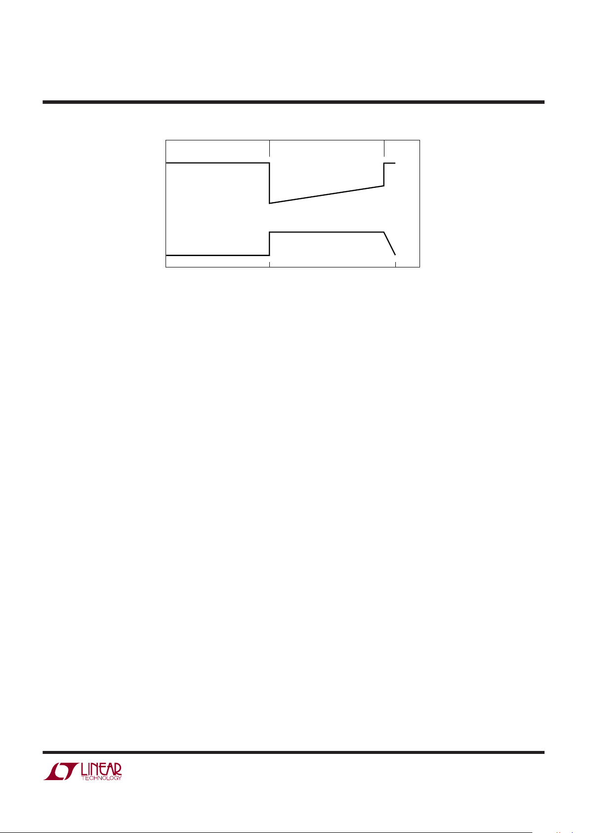
15
LTC4001
4001f
Battery charging current continues to drop as the V
BAT
rises, dropping to zero at V
FLOAT.
Because the voltage drop
in the LTC4001 is very low when charge current is highest,
power dissipation is also very low.
Thermal Calculations (PWM and Trickle Charging)
The LTC4001 operates as a linear charger when conditioning (trickle) charging a battery and operates as a high rate
buck battery charger at all other times. Power dissipation
should be determined for both operating modes.
For linear charger mode:
PD = (VIN – V
BAT
) • I
TRIKL
+ VIN • I
IN
where IIN is VIN current consumed by the IC.
Worst-case dissipation occurs for V
BAT
= 0, maximum VIN,
and maximum quiescent and trickle charge current. For
example with 5.5V maximum input voltage and 65mA
worst case trickle charge current, and 2mA worst-case
chip quiescent current:
P
D
= (5.5 – 0) • 65mA + 5.5 • 2mA = 368.5mW
LTC4001 power dissipation is very low if a current limited
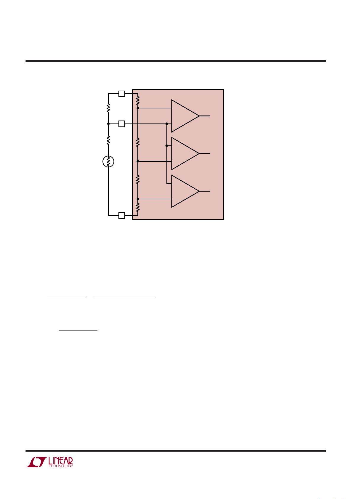
wall adapter is used and allowed to enter current limit.
When the wall adapter is in current limit, the voltage drop
across the LTC4001 charger is:
V
DROP
= I
LIMIT
• R
PFET
where I
LIMIT
is the wall adapter current limit and R
PFET
is
the on resistance of the topside PMOS switch.
The total LTC4001 power dissipation during current limited charging is:
PD = (V
BAT
+ V
DROP
) • (IIN + IP) + V
DROP
• I
LIMIT
where I
IN
is the chip quiescent current and IP is total
current flowing through the IDET and PROG programming
pins. Maximum dissipation in this mode occurs with the
highest V
BAT
that keeps the wall adapter in current limit
(which is very close to V
FLOAT
), highest quiescent current
I
IN
, highest PMOS on resistance R
PFET
, highest I
LIMIT
and
highest programming current I
P
.
Assume the LTC4001 is programmed for 2A charging and
200mA IDET and that a 1.5A wall adapter is being used:
I
LIMIT
= 1500mA, R
PFET
= 127mΩ, I
IN
= 2mA, IP = 4mA and
V
BAT
≈ V
FLOAT
= 4.242V
then:
V
DROP
= 1500mA • 127mΩ = 190.5mV
and:
P
D
= (4.242V + 0.1905V) • (2mA + 4mA) + 0.1905V
• 1500mA = 312mW
Power dissipation in buck battery charger mode may be
estimated from the dissipation curves given in the Typical
Performance Characteristics section of the data sheet.
This will slightly overestimate chip power dissipation
because it assumes all loss, including loss from external
components, occurs within the chip.
APPLICATIO S I FOR ATIO
WUUU
Figure 5. Charging Characteristic
LINEAR CHARGING
V
ADAPTER
V
IN
V
TRIKL
V
FLOAT
4001 F05
V
BAT
I
BAT
I
TRICKLE
WALL ADAPTER IN CURRENT LIMIT
V
BAT
+ V
DROP
I
LIMIT
PWM
CHARGING
Page 16

16
LTC4001
4001f
APPLICATIO S I FOR ATIO
WUUU
Insert the highest power dissipation figure into the following equation to determine maximum junction temperature:
T
J
= TA + (PD • 37°C/W)
The LTC4001 includes chip overtemperature protection. If
junction temperature exceeds 160°C (typical), the chip
will stop battery charging until chip temperature drops
below 150°C.
Using the LTC4001 in Applications Without a Battery
The LTC4001 is normally used in end products that only
operate with the battery attached (Figure 6). Under these
conditions the battery is available to supply load transient
currents. For indefinite operation with a powered wall
adapter there are only two requirements—that the average current drawn by the load is less than the high rate
charge current, and that V
BAT
stays above the trickle
charge threshold when the load is initially turned on and
during other load transients. When making this determination take into account battery impedance. If battery
voltage is less than the trickle charge threshold, the
system load may be turned off until V
BAT
is high enough
to meet these conditions.
The situation changes dramatically with the battery removed (Figure 7). Since the battery is absent, V
BAT
begins
at zero when a powered wall adapter is first connected to
the battery charger.
With a maximum load less than the
LTC4001 trickle charge current
, battery voltage will ramp
up until V
BAT
crosses the trickle charge threshold. When
this occurs, the LTC4001 switches over from trickle charge
to high rate (PWM) charge mode but initially delivers zero
current (because the soft-start pin is at zero). Battery
voltage drops as a result of the system load, crossing
below the trickle charge threshold. The charger re-enters
trickle charge mode and the battery voltage ramps up
again until the battery charger re-enters high rate mode.
The soft-start voltage is slightly higher this time around
(than in the previous PWM cycle). Every successive time
that the charger enters high rate (PWM) charge mode, the
soft-start pin is at a slightly higher voltage. Eventually high
rate charge mode begins with a soft-start voltage that
causes the PWM charger to provide more current than the
system load demands, and V
BAT
rapidly rises until the float
voltage is reached.
For battery-less operation, system load current should be
restricted to less than the worst case trickle charge current
(preferably less than 30mA) when V
BAT
is less than 3.15V
(through an undervoltage lockout or other means). Above
V
BAT
= 3.15V, system load current less than or equal to the
high rate charge current is allowed. If operation without a
battery is required, additional low-ESR output filtering
improves start-up and other load transients. Battery-less
start-up is also improved if a 10k resistor is placed in
series with the soft-start capacitor.
Figure 6. Typical Application
+
WALL
ADAPTER
LTC4001
BATTERY
CHARGER
SYSTEM
LOAD
Li-Ion
BATTERY
4001 F06
Page 17

17
LTC4001
4001f
APPLICATIO S I FOR ATIO
WUUU
Figure 7. Battery-Less Start-Up
024681012
TIME (ms)
14 16 18 20 22 24
4
3
2
1
0
V
BAT
(V)
024681012
TIME (ms)
14 16 18 20 22 24
500
250
0
V
SS
(mV)
024681012
TIME (ms)
4001 F07
14 16 18 20 22 24
PWM
CHARGE
TRICKLE
CHARGE
Page 18

18
LTC4001
4001f
Layout Considerations
Switch rise and fall times are kept under 5ns for maximum
efficiency. To minimize radiation, the SW pin and input
bypass capacitor leads (between PVIN and PGND) should
be kept as short as possible. A ground plane should be
used under the switching circuitry to prevent interplane
coupling. The Exposed Pad must be connected to the
ground plane for proper power dissipation. The other
paths contain only DC and/or 1.5MHz tri-wave ripple
current and are less critical.
Figure 8. 2A Li-Ion Battery Charger with 3Hr Timer, Temperature
Qualification, Soft-Start, Remote Sensing and C/10 Indication
With the exception of the input and output filter capacitors
(which should be connected to PGND) all other components that return to ground should be connected to
GNDSENS.
Recommended Components Manufacturers
For a list of recommend component manufacturers, contact the Linear Technology application department.
APPLICATIO S I FOR ATIO
WUUU
+
PROG
EN
FAULTTO µP
FROM µP
NTC
CHRG
PGND
PV
IN
V
INSENSE
BAT
BATSENS
IDET TIMER
R4
549Ω
C2
0.22µF
C3
0.1µF
L1: VISHAY DALE IHLP-2525AH-01
R3: NTC VISHAY DALE NTHS0603N02N1002J
C4
10µF
4001 F08
2AHr
4.2V
Li-Ion
C1
10µF
D1
LED
V
IN
4.5V TO 5.5V
SS
SW SENSE
LTC4001
L1
1.5µH
GNDSENS
R2
1k
R1
10k
R3
10k
AT 25°C
R5
549Ω
Page 19

19
LTC4001
4001f
Information furnished by Linear Technology Corporation is believed to be accurate and reliable.
However, no responsibility is assumed for its use. Linear Technology Corporation makes no representation that the interconnection of its circuits as described herein will not infringe on existing patent rights.
U
PACKAGE DESCRIPTIO
UF Package
16-Lead Plastic QFN (4mm × 4mm)
(Reference LTC DWG # 05-08-1692)
4.00 ± 0.10
(4 SIDES)
NOTE:
1. DRAWING CONFORMS TO JEDEC PACKAGE OUTLINE MO-220 VARIATION (WGGC)
2. DRAWING NOT TO SCALE
3. ALL DIMENSIONS ARE IN MILLIMETERS
4. DIMENSIONS OF EXPOSED PAD ON BOTTOM OF PACKAGE DO NOT INCLUDE
MOLD FLASH. MOLD FLASH, IF PRESENT, SHALL NOT EXCEED 0.15mm ON ANY SIDE
5. EXPOSED PAD SHALL BE SOLDER PLATED
6. SHADED AREA IS ONLY A REFERENCE FOR PIN 1 LOCATION
ON THE TOP AND BOTTOM OF PACKAGE
PIN 1
TOP MARK
(NOTE 6)
0.55 ± 0.20
1615
1
2
BOTTOM VIEW—EXPOSED PAD
2.15 ± 0.10
(4-SIDES)
0.75 ± 0.05
R = 0.115
TYP
0.30 ± 0.05
0.65 BSC
0.200 REF
0.00 – 0.05
(UF16) QFN 10-04
RECOMMENDED SOLDER PAD PITCH AND DIMENSIONS
0.72 ±0.05
0.30 ±0.05
0.65 BSC
2.15 ± 0.05
(4 SIDES)
2.90 ± 0.05
4.35 ± 0.05
PACKAGE OUTLINE
PIN 1 NOTCH R = 0.20 TYP
OR 0.35 × 45° CHAMFER
Page 20

20
LTC4001
4001f
LT 0406 • PRINTED IN THE USA
PART NUMBER DESCRIPTION COMMENTS
LT®1511 3A Constant Current/Constant Voltage Battery Charger High Efficiency, Minimum External Components to Fast Charge Lithium,
NIMH and NiCd Batteries, 24-Lead SO Package
LT1513 SEPIC Constant or Programmable Current/Constant Charger Input Voltage May Be Higher, Equal to or Lower Than Battery
Voltage Battery Charger Voltage, 500kHz Switching Frequency, DD Pak and TO-220 Packages
LT1571 1.5A Switching Charger 1- or 2-Cell Li-Ion, 500kHz or 200kHz Switching Frequency,
Termination Flag, 16- and 28-Lead SSOP Packages
LTC1729 Li-Ion Battery Charger Termination Controller Trickle Charge Preconditioning, Temperature Charge Qualification,
Time or Charge Current Termination, Automatic Charger and Battery
Detection, and Status Output, MS8 and SO-8 Packages
LT1769 2A Switching Charger Constant Current/Constant Voltage Switching Regulator, Input Current
Limiting Maximizes Charge Current, 20-Lead TSSOP and 28-Lead SSOP
Packages
LTC4002 Standalone Li-Ion Switch Mode Battery Charger Complete Charger for 1- or 2-Cell Li-Ion Batteries, Onboard Timer
Termination, Up to 4A Charge Current, 10-Lead DFN and SO-8 Packages
LTC4006 Small, High Efficiency, Fixed Voltage Li-Ion Battery Complete Charger for 2-, 3- or 4-Cell Li-Ion Batteries, AC Adapter
Charger with Termination Current Limit and Thermistor Sensor, 16-Lead Narrow SSOP Package
LTC4007 High Efficiency, Programmable Voltage Battery Complete Charger for 3- or 4-Cell Li-Ion Batteries, AC Adapter Current
Charger with Termination Limit, Thermistor Sensor and Indicator Outputs, 24-Lead SSOP Package
LTC4008 4A, High Efficiency, Multi-Chemistry Battery Charger Complete Charger for 2- to 6-Cell Li-Ion Batteries or 4- to 18-Cell Nickel
Batteries, Up to 96% Efficiency, 20-Lead SSOP Package
RELATED PARTS
Linear Technology Corporation
1630 McCarthy Blvd., Milpitas, CA 95035-7417
(408) 432-1900 ● FAX: (408) 434-0507
●
www.linear.com
© LINEAR TECHNOLOGY CORPORATION 2006
 Loading...