

Page 1

LINEAR TECHNOLOGY
LINEAR TECHNOLOGY
LINEAR TECHNOLOGY
JANUARY 2009 VOLUME XVIII NUMBER 4
IN THIS ISSUE…
COVER ARTICLE
2-Phase, Non-Synchronous Boost
Controller Simplifies Design of
High Voltage, High Current Supplies
...........................................................1
Muthu Subramanian and Tick Houk
Linear in the News… ...........................2
DESIGN FEATURES
Reliable Precision Voltage Reference
with 5ppm/°C Drift is Factory Trimmed
and Tested at –40°C, 25°C and 125°C
...........................................................7
Michael B. Anderson and Brendan Whelan
Ultralow Noise 15mm ×15mm × 2.8mm
µModule™ Step-Down Regulators Meet
the Class B of CISPR 22 and Yield
High Efficiency at up to 36V
Judy Sun, Jian Yin, Sam Young and Henry
Zhang
Dual Hot Swap™ Controller Brings
Digital Monitoring to AdvancedTCA,
µTCA and AMC Applications ..............15
Josh Simonson
±32V Triple-Output Supply for LCDs,
CCDs and LEDs Includes Fault
Protection in a 3mm × 3mm QFN ......20
Eko T Lisuwandi
PD Interface for PoE+ Includes 25.5W
Classification and Protection Features
in a Low Profile 4mm × 3mm DFN
.........................................................26
Kirk Su
DESIGN IDEAS
....................................................
(complete list on page 30)
Design Tools ......................................43
Sales Offices .....................................
..........10
IN
30–42
44
2-Phase, Non-Synchronous
Boost Controller Simplifies
Design of High Voltage,
High Current Supplies
by Muthu Subramanian and Tick Houk
Introduction
Due to an increasing need for high
power step-up power supplies in automotive and industrial applications,
Linear Technology has recently introduced the LTC3862 family of 2-phase,
single output non-synchronous boost
DC/DC controllers. The LTC3862
provides a flexible, high performance
step-up controller in three convenient
package options: GN24, 5mm × 5mm
24-pin exposed pad QFN and 24-pin
exposed pad TSSOP. The LTC3862 is
optimized for power MOSFETs that
require 5V gate drive, whereas the
LTC3862-1 is designed for 10V gate
drive MOSFETs.
The LTC3862 utilizes a fixed frequency, peak current mode control
topology to drive ground-referenced
power MOSFETs, each with a current sense resistor in its source. The
use of a precision transconductance
(gm) error amplifier allows for easy
loop compensation and facilitates the
parallel connection of several ICs in
multiphase applications. The operating frequency can be programmed
from 75kHz to 500kHz using a single
resistor, and a phase lock loop allows
the switching frequency to be synchronized to an external clock over a
50kHz to 650kHz range.
The LTC3862 is a versatile
control IC optimized for a
wide variety of step-up
DC/DC converter
applications. This makes
it easy to optimize
efficiency, size and weight
of the power supply, while
keeping component and
manufacturing costs low.
A 24V, 5A
Car Audio Power Supply
Today’s high end car audio systems
require significant power to drive
upwards of seven speakers inside
the passenger compartment. High
frequency speakers such as tweeters
are generally very efficient, but low
frequency drivers such as subwoofers
require substantial power to achieve
high volume. In addition to the need
for high power, the car audio system
should be itmmune to changes in
the battery voltage. These requirements can be met through the use
of a step-up converter for the power
continued on page 3
L
, LT, LTC, LTM, Burst Mode, OPTI-LOOP, Over-The-Top and PolyPhase are registered trademarks of Linear Technology
Corporation. Adaptive Power, Bat-Track, BodeCAD, C-Load, DirectSense, Easy Drive, FilterCAD, Hot Swap, LinearView,
µModule, Micropower SwitcherCAD, Multimode Dimming, No Latency ΔΣ, No Latency Delta-Sigma, No R
Filter, PanelProtect, PowerPath, PowerSOT, SmartStart, SoftSpan, Stage Shedding, SwitcherCAD, ThinSOT, TimerBlox, True
Color PWM, UltraFast and VLDO are trademarks of Linear Technology Corporation. Other product names may be trademarks
of the companies that manufacture the products.
, Operational
SENSE
Page 2
LTC3862, continued from page 1
SENSE1
+
3V8
SLOPE
BLANK
CLKOUT
SYNC
PLLFLTR
PHASEMODE
D
MAX
10nF
SENSE1
–
SENSE2
–
SENSE2
+
RUN
FREQ
SS
V
IN
45.3k 24.9k
84.5k
10Ω
V
IN
5V TO 24V
D1
MBRD835L
D2
MBRD835L
10Ω
L2
4.2µH
CDEP145-4R2
ITH
SGND
V
OUT
6.98k
FB
26.7k
130k
10nF
1µF
1nF
22µF 25V
0.007Ω
1W
Q1
Si7386DP
Q2
Si7386DP
0.007Ω
1W
V
OUT
24V
5A (MAX)
100µF
35V
100µF
35V
22µF 25V
22µF 25V
10µF 50V
LTC3862
1nF
100pF
INTV
CC
GATE1
GATE2
PGND
4.7µF
10nF
10µF 50V
10µF 50V
10µF 50V
L1
4.2µH
CDEP145-4R2
+
+
LOAD CURRENT (mA)
EFFICIENCY (%)
POWER LOSS (mW)
100
95
90
75
10000
1000
100
85
80
10000
100 1000
EFFICIENCY
POWER LOSS
VIN = 12V
V
OUT
= 24V
I
LOAD
5A/DIV
I
L1
5A/DIV
I
L2
5A/DIV
V
OUT
500mV/DIV
500µs/DIVVIN = 12V
V
OUT
= 24V
I
LOAD
= 2A TO 5A
DESIGN FEATURES L
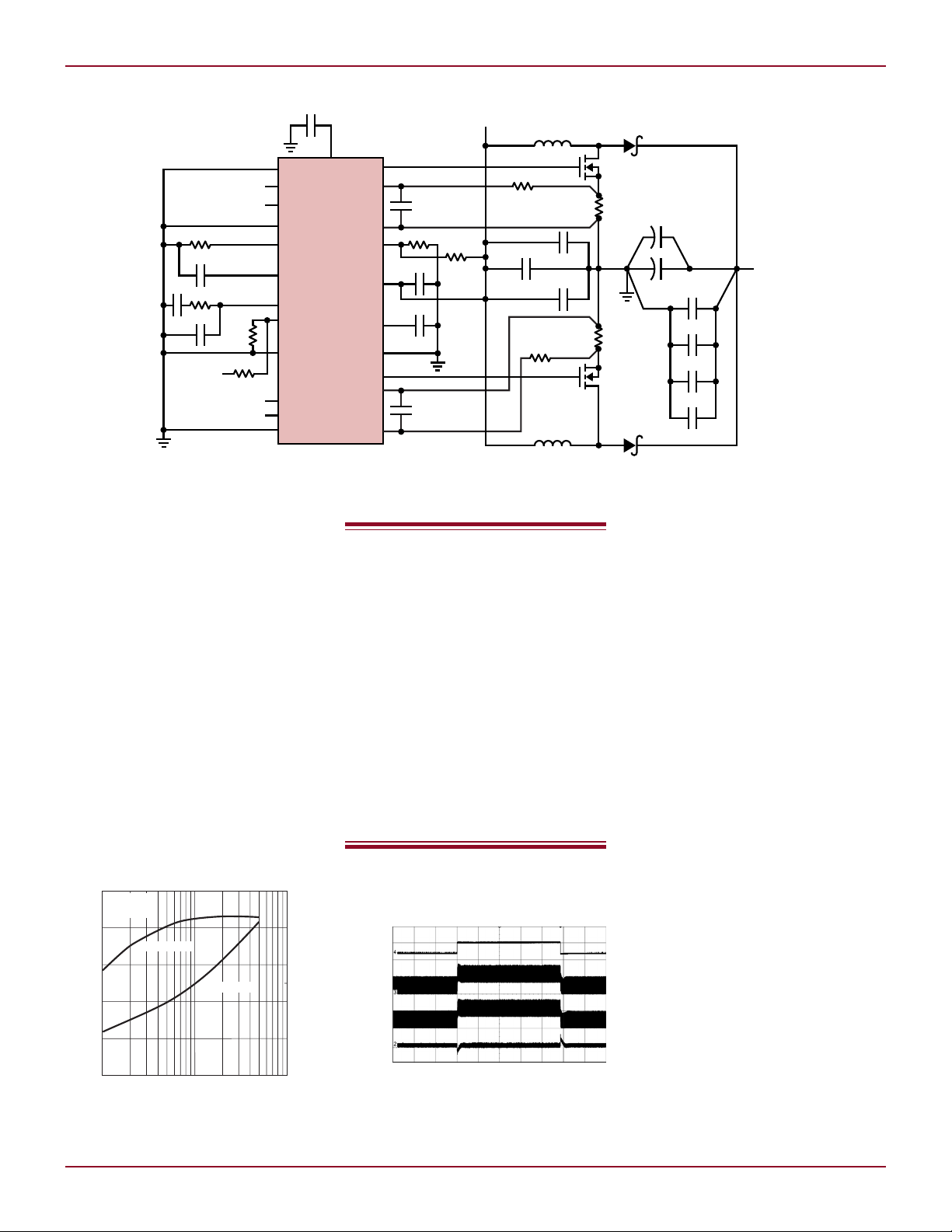
Figure 1. A 120W 2-phase, 24V/5A output car audio power supply
amplifiers. Figure 1 shows a 2-phase,
24V/5A output audio power supply
that operates from a car battery, and
Figure 2 shows the efficiency curve
for this converter.
A 2-phase design with an operating
frequency of 300kHz allows the use of
significantly smaller output capacitors
and inductors than a single-phase
design. To keep the output ripple
voltage below 60mV peak-to-peak and
satisfy the RMS ripple current demand,
a combination of two 100µF, 35V
aluminum electrolytic capacitors are
connected in parallel with four 10µF,
50V ceramic capacitors. The 4.2µH,
10.6A inductor (CDEP145-4R2) from
Sumida Inductors is chosen for its high
Figure 2. Efficiency and power loss vs load
current for the 120W car audio power supply
Linear Technology Magazine • January 2009
A 2-phase design with an
operating frequency of
300kHz allows the use of
significantly smaller output
capacitors and inductors
than a single-phase design.
Also, the output current
of this converter can
easily be scaled by adding
additional power stages
and controllers, without
modifying the basic design.
Figure 3. Inductor current waveforms in load
step show accurate current matching between
load sharing channels
saturation current rating and surface
mount package design.
The MOSFET is a Vishay Si7386DP,
which has a maximum R
DS(ON)
of 7mΩ
at VGS = 10V and 9.5mΩ at VGS =
4.5V. The 35V, 8A Schottky from On
Semiconductor (MBRD835L) offers
surface mount capability and small
size. It should be noted that the output
current of a converter such as this can
easily be scaled by adding additional
power stages and controllers, without
modifying the basic design.
Excellent Channel-to-Channel
Current Matching Ensures a
Balanced Thermal Design
In order to provide the best channelto-channel inductor current matching,
the LTC3862 is designed to make the
transfer function from the output of
the error amplifier (the ITH pin) to the
current comparator inputs (SENSE+
and SENSE– pins) as accurate as
possible. The specification for the
maximum current sense threshold is
75mV, and the channel-to-channel
(V
tion is ±10mV, over the –40°C to 150°C
temperature range. This excellent
matching ensures balanced inductor
currents and a thermally stable design,
even with multiple regulators daisychained together. Figure 3 shows how
SENSE1
– V
) mismatch specifica-
SENSE2
3
Page 3
L DESIGN FEATURES
SENSE1
+
SLOPE
BLANK
CLKOUT
SYNC
PLLFLTR
PHASEMODE
D
MAX
10nF
SENSE1
–
SENSE2
–
SENSE2
+
RUN
FREQ
SS
V
IN
45.3k 24.9k
150k
10Ω
V
IN
8.5V TO 28V
D1
B3100
D2
B3100
10Ω
L2
58µH
PA2050-583
ITH
SGND
V
OUT
5.62k
FB
45.3k
324k
0.1µF
1µF
6.8µF 50V
0.020Ω
1W
Q1
HAT2267H
Q2
HAT2267H
0.020Ω
1W
V
OUT
72V
47µF
100V
47µF
100V
6.8µF 50V
6.8µF 50V
2.2µF
100V
s6
LTC3862-1
1.5nF
100pF
INTV
CC
GATE1
GATE2
PGND
4.7µF
10nF
L1
58µH
PA2050-583
+
+
3V8
1nF
SYNC
10V/DIV
GATE1
10V/DIV
GATE2
10V/DIV
CLKOUT
10V/DIV
2µs/DIVVIN = 12V
V
OUT
= 48V 1A
PHASEMODE = SGND
SW1
10V/DIV
SW2
10V/DIV
I
L1
1A/DIV
I
L2
1A/DIV
1µs/DIVVIN = 17V
V
OUT
= 24V
LIGHT LOAD (10mA)
2.5µs/DIVVIN = 24V
V
OUT
= 48V, 1.5A
SW1
50V/DIV
SW2
50V/DIV
V
OUT
100mV/DIV
AC COUPLED
I
L1
5A/DIV
I
L2
5A/DIV
SW1
50V/DIV
SW2
50V/DIV
I
L1
2A/DIV
I
L2
2A/DIV
1µs/DIVVIN = 12V
V
OUT
= 48V
I
LOAD
= 100mA
I
L
5A/DIV
V
OUT
20V/DIV
500µs/DIV
VIN = 24V
V
OUT
= 72V
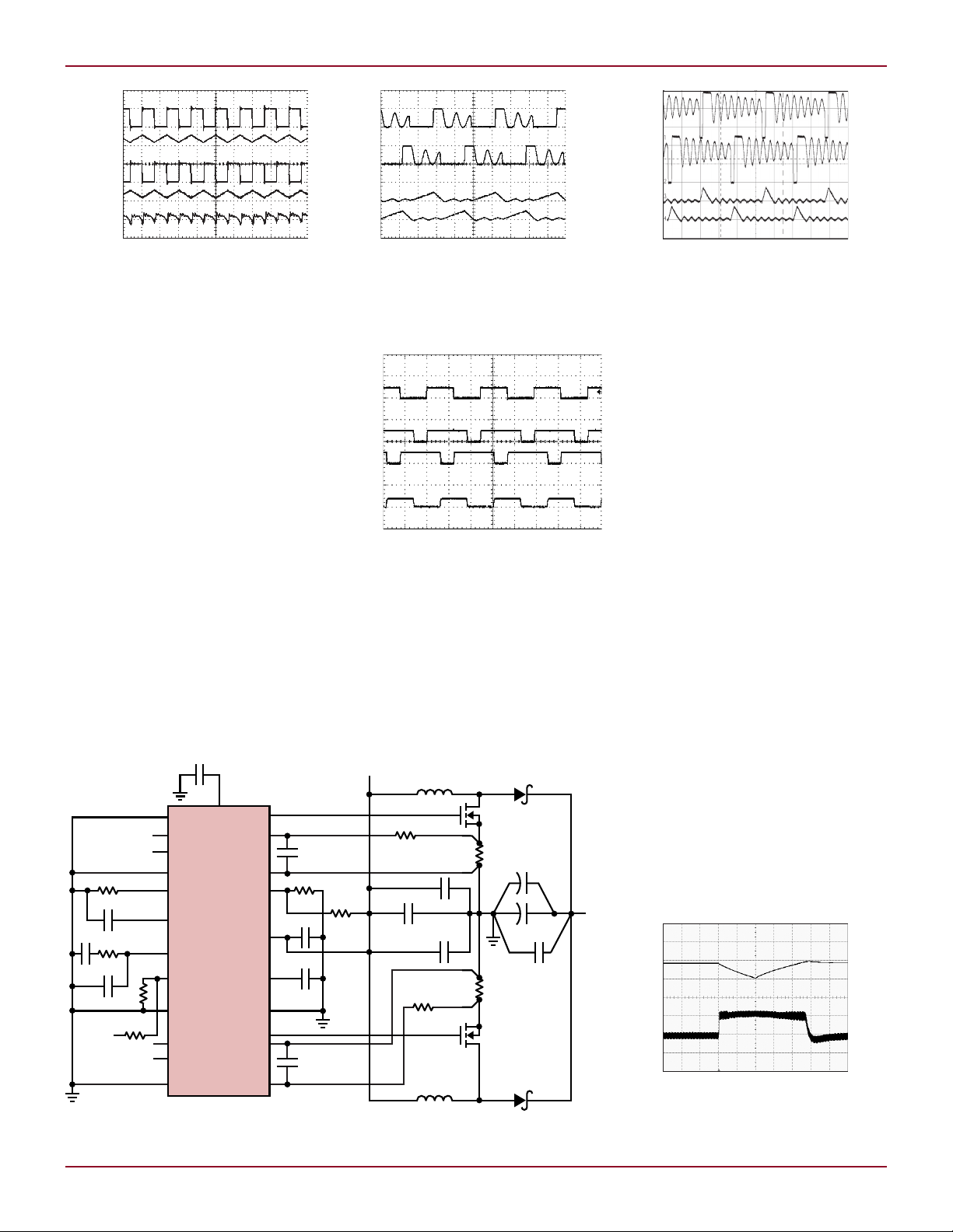
Figure 4. Inductor current and switch node
voltage waveforms at heavy load, continuous
conduction mode (CCM)
well matched the inductor currents are
for the car audio power supply during
a load step.
Constant Frequency
Operation over a Wide
Load Current Range
Constant frequency operation eases
the task of input and output filter
design, and prevents a power supply
from becoming audible at light load. At
heavy load, the inductor currents are
generally continuous (CCM), as shown
in Figure 4. At light load, the inductor
current will go discontinuous (DCM),
as shown in Figure 5. When the load
current drops below what can be supported by the minimum on-time of the
converter (approximately 180ns), the
controller will begin to skip cycles in
order to maintain output regulation,
Figure 8. An 8.5V–28V input, 72V/1.5A output low emissions diesel fuel injector actuator supply
4
Figure 5. Inductor and switch node voltage
waveforms at light load, discontinuous
Figure 6. Inductor and switch node voltage
waveforms at light load (pulse-skipping)
conduction mode (DCM)
the better, since constant frequency
operation is maintained down to this
threshold. In Figure 6 the onset of
pulse-skipping occurs at a relatively
low 0.2% of the maximum load current.
For systems where synchronization
to an external clock is required, the
LTC3862 contains a phase lock loop
(PLL). Figure 7 illustrates the switching waveforms with an external sync
signal applied to the SYNC pin.
Figure 7. Synchronizing the LTC3862 to an
external clock using the phase lock loop
Strong Gate Drivers and a
High Current Internal LDO
as shown in Figure 6. This is a normal
operating condition that doesn’t cause
any problems in the system, as long as
the peak inductor current is low.
In general, the lower the load cur-
rent at the onset of pulse-skipping,
Complete the Package
In high output voltage systems, switching losses in the power MOSFETs can
sometimes exceed the conduction
losses. In order to reduce switching losses as much as possible, the
LTC3862 incorporates strong gate
drivers. The PMOS pull-up transistor has a typical R
the NMOS pull-down transistor has
a typical R
of 0.7Ω. In addition
DS(ON)
to reducing switching losses, these
strong gate drivers allow two power
MOSFETs to be connected in paral-
Figure 9. Load step waveforms for
diesel fuel injector actuator supply
Linear Technology Magazine • January 2009
of 2.1Ω, and
DS(ON)
Page 4
DESIGN FEATURES L
SENSE1
+
SLOPE
BLANK
CLKOUT
SYNC
PLLFLTR
PHASEMODE
D
MAX
10nF
ON/OFF
CONTROL
SENSE1
–
SENSE2
–
SENSE2
+
RUN
FREQ
SS
V
IN
45.3k
10Ω
V
IN
4.5V TO 5.5V
D1
MBRB2515LT41
D2
MBRB2515LT41
10Ω
L2
2.7µH
CDEP145-2R7
ITH
SGND
V
OUT
18.7k
FB
3.83k
165k
10nF
1µF
33µF 10V
33µF 10V
33µF 10V
0.005Ω
1W
Q1
HAT2165H
Q3
HAT2165H
0.005Ω
1W
V
OUT
12V
15A
220µF
16V
220µF
16V
LTC3862
10nF
330pF
INTV
CC
GATE1
GATE2
PGND
4.7µF
10nF
15µF 25V
15µF 25V
15µF 25V
15µF 25V
L1
2.7µH
CDEP145-2R7
+
+
SENSE1
+
SLOPE
BLANK
CLKOUT
SYNC
PLLFLTR
PHASEMODE
D
MAX
10nF
SENSE1
–
SENSE2
–
SENSE2
+
RUN
FREQ
SS
V
IN
45.3k
10Ω
D1
MBRB2515LT41
D2
MBRB2515LT41
10Ω
L2
2.7µH
CDEP145-2R7
ITH
SGND
FB
10k
1µF
33µF 10V
33µF 10V
33µF 10V
0.005Ω
1W
Q1
HAT2165H
Q3
HAT2165H
0.005Ω
1W
220µF
16V
220µF
16V
LTC3862
10nF
INTV
CC
GATE1
GATE2
PGND
4.7µF
330pF
10nF
15µF 25V
15µF 25V
15µF 25V
15µF 25V
L1
2.7µH
CDEP145-2R7
+
+
3V8
1nF
3V8
1nF
lel for each channel in high current
applications.
In order to simplify operation in
single-supply systems, the LTC3862
includes a 5V low dropout regulator
(LDO) that can support output currents up to 50mA. The use of a PMOS
output transistor ensures that the full
supply voltage is available for driving
the power MOSFETs under low supply
conditions, such as during automotive cold cranking. An undervoltage
lockout circuit detects when the LDO
output voltage falls below 3.3V and
shuts off the gate drivers, thereby
protecting the power MOSFETs from
switching at low VGS.
The LTC3862 is capable of operation
over a 4V to 36V input voltage range,
making it suitable for a wide variety
of boost applications.
Lower Emissions Diesel Fuel
Injection: A 8.5V–28V Input,
72V, 1.5A Output Boost
Tomorrow’s low emissions diesel
fuel injection systems require more
precise and faster actuation of the
fuel injectors than do their gasoline
counterparts. Stepping up the voltage
of the system is an easy way to achieve
fast actuation by increasing di/dt in
the actuator, since the energy stored
on a capacitor is CV2/2. Boosting the
car battery voltage from 13V to 72V significantly increases the di/dt, enabling
faster actuation. The actuation of the
injector typically discharges the supply
capacitor by 10V–20V, after which the
boost converter recharges the output
cap to 72V. Figure 8 illustrates this
8.5V to 28V input, 72V/1.5A output
2-phase boost converter. Figure 9 illustrates the load step for a simulated
injector.
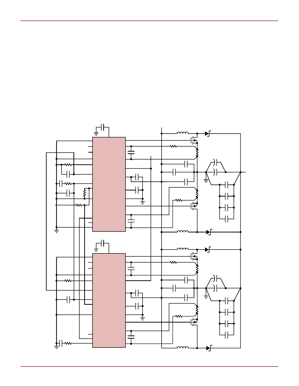
Figure 10. A 4-phase, 12V/15A industrial power supply that operates from a 5V input
Linear Technology Magazine • January 2009
5
Page 5
L DESIGN FEATURES
V
IN
5V/DIV
IL1 MASTER
5A/DIV
IL2 MASTER
5A/DIV
IL1 SLAVE
5A/DIV
IL2 SLAVE
5A/DIV
V
OUT
10V/DIV
1ms/DIVVIN = 5V
V
OUT
= 12V
R
LOAD
= 10Ω
I
LOAD
2.5A-5A
5A DIV
IL1 MASTER
5A/DIV
IL2 MASTER
5A/DIV
IL1 SLAVE
5A/DIV
IL2 SLAVE
5A/DIV
V
OUT
200mV/DIV
250µs/DIVVIN = 5V
V
OUT
= 12V
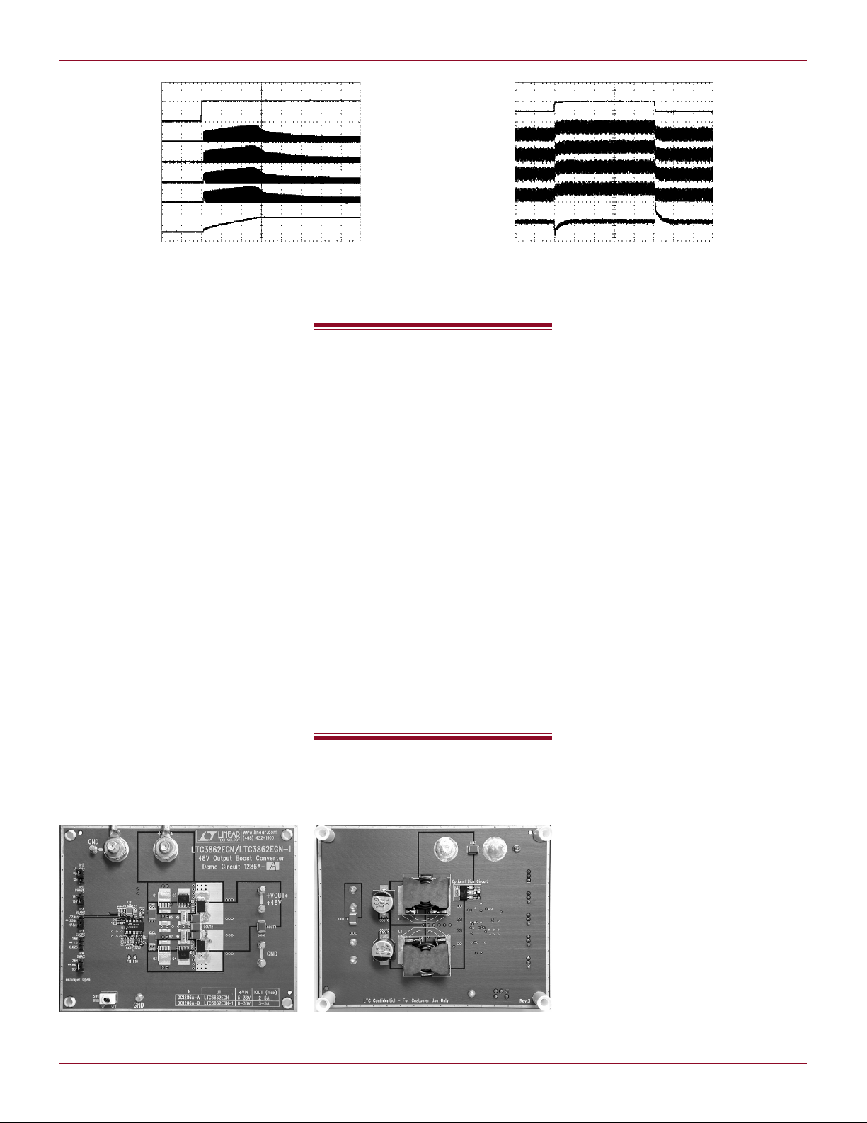
Figure 11. Power supply start-up waveforms for
4-phase, 12V/15A industrial power supply
This power supply operates at a
switching frequency of 300kHz in order
to reduce switching losses and uses a
57.8µH, 5A inductor (PA2050-583). An
80V Renesas HAT2267H MOSFET was
chosen for this application, in order
to provide sufficient guardband above
the 72V output. The MOSFET has a
maximum R
of 13mΩ at VGS =
DS(ON)
10V. The Diodes Inc surface mount
diode (B3100) was chosen for the 3A
output current level. A combination
of a two 47µF, 100V electrolytic and
six 2.2µF, 100V low ESR ceramic capacitors are used to reduce the output
ripple to below 100mV peak-to-peak
and satisfy the RMS ripple current
requirement.
A 4-Phase, 5V Input,
12V/15A Output,
Industrial Power Supply
Figure 10 illustrates an industrial
power supply that converts a 5V input to a 12V output at up to 15A of
load current. The use of four phases
greatly eases the task of choosing
the power components, and reduces
output ripple significantly. Figure 11
Figure 12. Load step waveforms for 4-phase,
12V/15A industrial power supply
In high output voltage
systems, switching losses
in the power MOSFETs
can sometimes exceed the
conduction losses. In order
to reduce switching losses
as much as possible, the
LTC3862 incorporates
strong gate drivers. The
PMOS pull-up transistor has
a typical R
DS(ON)
of 2.1Ω,
and the NMOS pull-down
transistor has a typical
R
of 0.7Ω. In addition to
DS(ON)
reducing switching losses,
these strong gate drivers
allow two power MOSFETs to
be connected in parallel for
high current applications.
shows the start-up waveforms for this
converter. Figure 12 shows the load
step waveforms.
Multiphase operation is made possible using the PHASEMODE, SYNC
and CLKOUT pins. The PHASEMODE
pin controls the phase relationship
between GATE 1 and GATE 2, as
well as between GATE 1 and CLKOUT. The CLKOUT pin of a master
controller is connected to the SYNC
pin of a slave, where the phase lock
loop ensures proper synchronization.
The PHASEMODE pin can be used to
program 2-, 3-, 4-, 6- and 12-phase
operation.
48V/5A Demo Circuit
The DC1286A demonstration circuit
board is designed for high power applications, providing a 48V/5A output
using the GN24 package option of the
LTC3862 or LTC3862-1. The 6-layer
PCB design ensures proper routing of
the SENSE lines, and exhibits minimal
jitter even at 50% duty cycle. Jumpers are provided to easily change the
BLANK time, PHASE, maximum duty,
and SLOPE compensation. There is
an optional onboard 12V VIN supply
to power the IC, and the component
footprint provides flexibility to use
various inductors, MOSFET’s and
diodes.
Conclusion
The LTC3862 is a versatile control IC
optimized for a wide variety of stepup DC/DC converter applications. Its
Figure 13. 48V/5A output, high power demonstration circuit
6
flexible, high performance operation
and three convenient package options
make it possible to optimize efficiency,
size and weight of the power supply,
while keeping the total component and
manufacturing costs low.
Linear Technology Magazine • January 2009
L
 Loading...