

Page 1
DESCRIPTION
DEMO MANUAL DC2199A-A
LTC3765/LTC3766
360W Isolated Forward Converter
with Synchronous Rectification
Demonstration circuit 2199A-A is a 360W isolated forward converter
with synchronous rectification featuring
the LTC3765/LTC3766. It produces a regulated 12V, 30A
output from an input voltage range of 36V to 60V.
This circuit was designed to demonstrate the high levels
of performance, efficiency, and small solution size attain
able using
converter
and other applications. It has a 4.7in
these parts in an active-clamp-reset forward
power supply, suitable for telecom, industrial,
2
solution footprint
ciency exceeding 96%. Secondary-side control eliminates
complex opto-coupler feedback, providing fast transient
response with minimum output capacitance. For other
output requirements, see the LTC3766 data sheet or
contact the LT C sales.
-
Design files for this circuit board are available at
http://www.linear.com/demo/DC2199A-A
L, LT, LTC, LTM, Linear Technology and the Linear logo are registered trademarks of Linear
Technology Corporation. All other trademarks are the property of their respective owners.
area. Synchronous rectification helps to attain an effi-
PERFORMANCE SUMMARY
SYMBOL PARAMETER CONDITIONS MIN TYP MAX UNITS
V
IN
V
OUT
I
OUT
f
SW
V
OUT(P-P)
I
REG
P
OUT/PIN
Input Supply Range 36 60 V
Output Voltage 11.76 12.0 12.24 V
Output Current Range, Continuous 200LFM 0 30 A
Switching (Clock) Frequency 200 kHz
Output Ripple VIN = 24V, I
Output Regulation Line and Load (36VIN to 60VIN, 0A
Efficiency (See Figure 3) VIN =48V, I
Isolation Basic 1500 VDC
Approximate Solution Size Component Area × Top Component Height 4.7in
Specifications are at TA = 25°C
= 30A (20MHz BW) 60 mV
OUT
to 30A
OUT
= 30A 96 %
OUT
) ±0.02 %
OUT
2
× 0.6 Inches
P-P
dc2199aafa
1
Page 2

DEMO MANUAL DC2199A-A
OPERATING PRINCIPLES
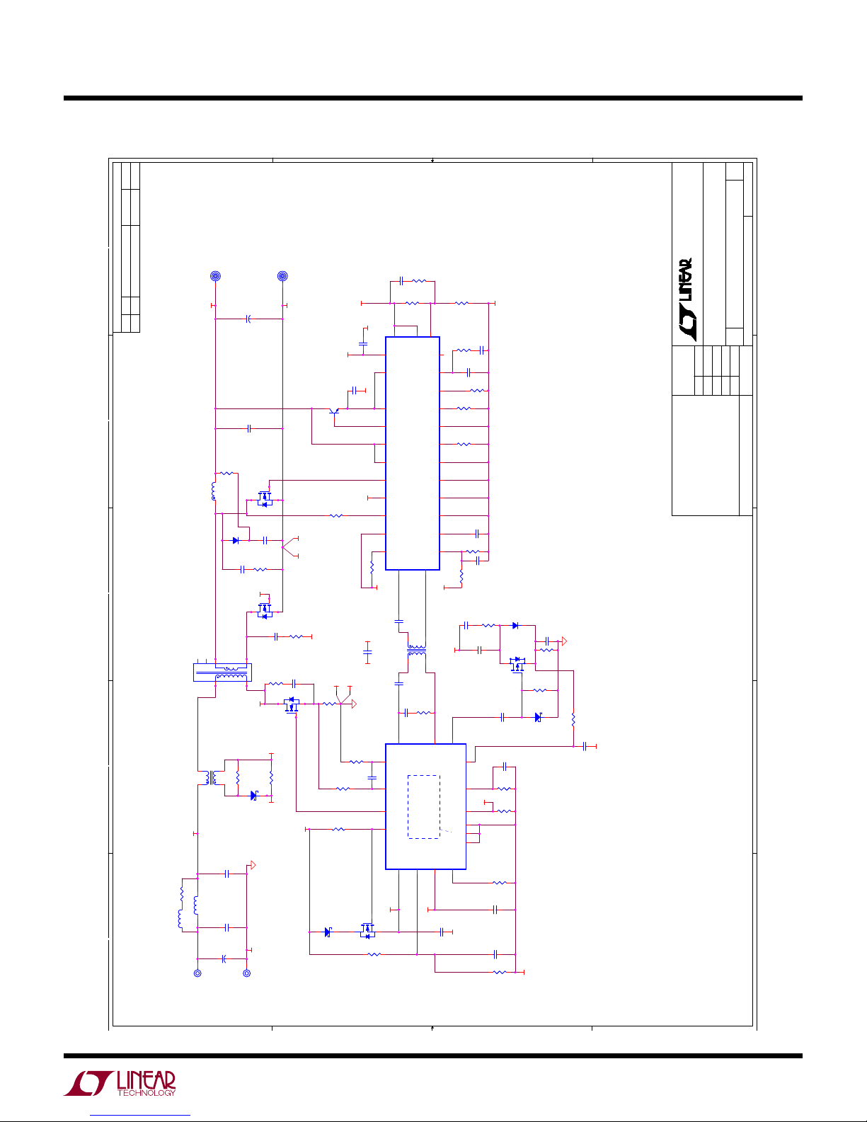
The LTC3765 active clamp forward controller and gate
driver is used on the primary and provides start-up, gate
drive, and protection functions. Once start-up is accom
plished, the LTC3766 high efficiency, secondary-side
synchronous forward controller takes over, and provides
the LTC3765 with timing information and bias power
through a small pulse transformer.
When input voltage is applied, the LTC3765 commences
soft-start of the output voltage. When the output reaches
the RUN threshold, the LTC3766 comes alive and takes
control by sending encoded PWM gate pulses to the
LTC3765 through T2. These pulses also provide primary
bias power efficiently over a wide input voltage range.
The transition from primary to secondary control occurs
at some fraction of the nominal output voltage. From then
on, operation and design is reduced to that of a simple
-
QUICK START PROCEDURE
buck converter. Secondary control eliminates delays, tames
large-signal overshoot, and reduces output capacitance
needed to meet transient response requirements.
An optional LC filter stage on the input lowers RMS input
current. The filter must have output impedance that is less
than the converter input impedance to assure stability.
This may require a damping impedance, which is provided
by R1. (See Linear Technology Application Note 19 for a
discussion of input filter stability.) R1 is coupled through
a tiny 2mm × 2mm inductor L1, and provides damping
with arbitrarily low source impedance. For bench testing,
an electrolytic capacitor has been added at the input ter
minals to provide suitable ripple current capability. The
values
below the converter switching frequency, thus avoiding
high circulating currents in the filter.
selected have a filter resonant frequency that is
-
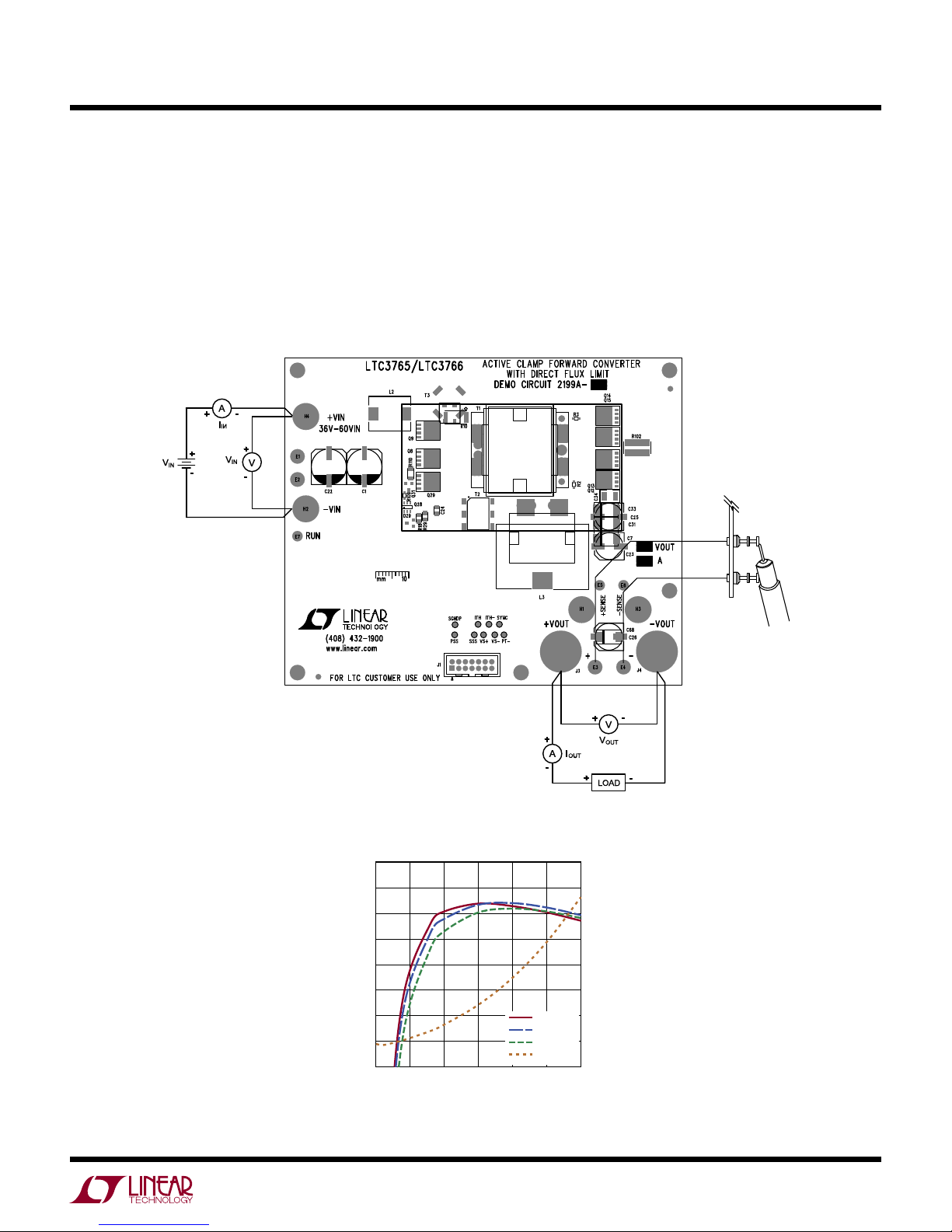
Demonstration circuit 2199A-A is easy to set up to evalu
ate the
Figure
follow the procedure below:
NOTE: When measuring the output voltage ripple, care must
be taken to avoid a long ground lead on the oscilloscope
probe. Measure the output voltage ripple
probe
capacitor as shown in Figure 1.
1. Set an input power supply that is capable of 36V to 60V
2. Direct an airflow of 200LFM across the unit for sustained
3. With power off, connect the supply to the input terminals
performance of the LTC3765/LTC3766. Refer to
1 for proper measurement equipment setup and
by touching the
tip and ground ring directly across the last output
to 36V. Then turn off the supply.
operation at full load.
and –VIN.
+V
IN
a. Input voltages lower than 36V can keep the converter
from turning on due to the undervoltage lockout
feature of the LTC3765/LTC3766.
-
b. If efficiency measurements are desired, an ammeter
capable of measuring 15ADC or a resistor shunt can
be put in series with the input supply in order to
measure the DC2199A-A’s input current.
c. A voltmeter with a capability of measuring at least
60V can be placed across the input terminals in order
to get an accurate input voltage measurement.
4. Turn on the power at the input.
NOTE: Make sure that the input voltage never ex
ceeds 60V.
Check for the proper output voltage of 12V. Turn off
5.
the power at the input.
6. Once the proper output voltages are established, con
nect a variable load capable of sinking 30A at 12V to
output terminals +V
the
for 0A.
a. If efficiency measurements are desired, an ammeter
or a resistor shunt that is capable of handling 30ADC
can be put in series with the output load in order to
measure the DC2199A-A’s output current.
OUT
and –V
. Set the current
OUT
-
-
2
dc2199aafa
Page 3
QUICK START PROCEDURE
EFFICIENCY? (%)
98
POWER DISSIPATION (W)
18
dc2199aa F02
DEMO MANUAL DC2199A-A
b. A voltmeter with a capability of measuring at least 12V
can be placed across the output terminals in order
to get an accurate output voltage measurement.
7. Turn on the power at the input.
NOTE. If there is no output, temporarily disconnect the
load to make sure that the load is not set too high.
8. Once the proper output voltage is again established,
adjust the load within the operating range and observe
the output voltage regulation, ripple voltage, efficiency
and other desired parameters.
Figure 1. Proper Measurement Equipment Setup
97
96
95
94
93
92
91
90
0
10 205 15
I
OUT
(A)
36V
48V
60V
48V
IN
IN
IN
IN_PD
16
14
12
10
8
6
4
2
3025
Figure 2. Efficiency and Power Dissipation
dc2199aafa
3
Page 4
DEMO MANUAL DC2199A-A
QUICK START PROCEDURE
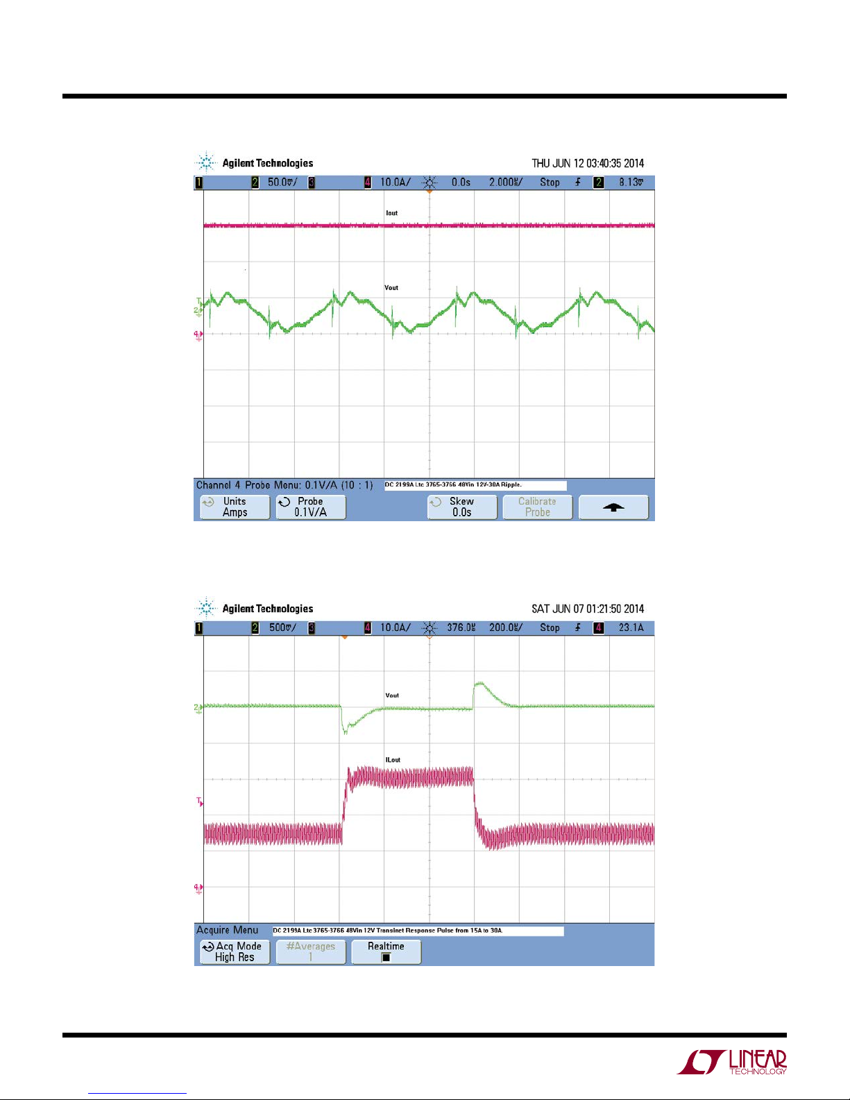
Figure 3. Output Ripple at 48VIN and 30A
(50mV, 10A, 2µs/DIV, 20MHz)
OUT
Figure 4. Transient Response Waveform at 48V
4
and 15A to 30A to 15A
IN
(10A, 500mV, 200µs/DIV)
OUT
dc2199aafa
Page 5
QUICK START PROCEDURE
DEMO MANUAL DC2199A-A
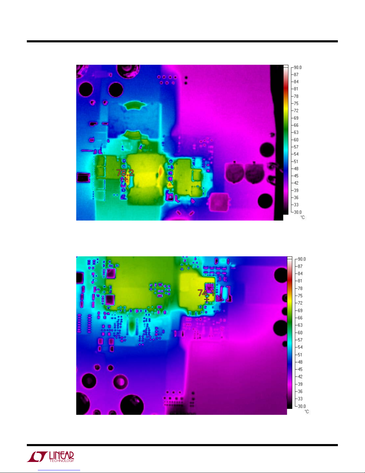
Figure 5. Thermal Map, Front Side at 48VIN and 30A
(TA = 25°C, 200LFM)
OUT
Figure 6. Thermal Map, Back Side at 48V
and 30A
IN
(TA = 25°C, 200LFM)
OUT
dc2199aafa
5
Page 6

DEMO MANUAL DC2199A-A
PARTS LIST
ITEM QTY REFERENCE PART DESCRIPTION MANUFACTURER/PART NUMBER
Required Circuit Components
1 2 C1, C22 Cap., Alum., Elect., 33µF, 80V, CAP-10X12.5 PANASONIC, EEHZA1K330P
2 5 C2, C3, C4, C5, C6 CAP., X7R, 4.7µF, 100V, 10%, 1210 MURATA, GRM32ER72A475KE14
3 4 C7, C31, C33, C68 CAP., POSCAP, 150µF, 16V, 20%, 7343 PANASONIC, 16TQC150MYF
4 1 C10 CAP., X7R, 2.2nF, 630V, 5%, 1206 MURATA, GRM31A7U2J222JW31
5 1 C11 CAP., X7R, 0.015µF, 25V, 10%, 0603 AVX, 06033C153K AT2A
6 2 C24, C71 CAP., X7R, 1.0µF, 16V, 10%, 0805 MURATA, GRM21BR71C105KA01
7 1 C30 CAP., X7R, 2200pF, 250V, 10%, 1812 MURATA, GA343QR7GD222KW01L
8 1 C34 CAP., X5R, 22µF, 16V, 20%, 1206/1210 MURATA, GRM32ER71C226MEA8L
9 1 C51 CAP., C0G, 470pF, 630V, 5%, 1206 MURATA, GRM31A5C2J471JW01
10 1 C66 CAP., X7R, 0.047µF, 200V, X7R, 10% 1206 MURATA, GRM31CR72D473KW03
11 1 C69 CAP., X7R, 1.5nF, 630V, 5%, 1206 MURATA, GRM31A7U2J152JW31
12 2 C70, C76 CAP., X7R, 3.3nF, 25V, 10%, 0603 AVX, 06033C332KAT2A
13 2 C72, C102 CAP., X7R, 0.1µF, 25V, 10%, 0805 AVX, 08053C104KAT2A
14 4 C55, C73, C80, C119 CAP., X7R, 1nF, 25V, 10%, 0603 MURATA, GRM188R71E102KA01
15 1 C75 CAP., NPO, 100pF, 25V, 5%, 0603 AVX, 06033A101J AT2A
16 1 C77
17 1 C78 CAP., NPO, 0.033µF, 25V, 5%, 0805 TDK, C2012C0G1E333J
18 1 C79 CAP., X7R, 4.7nF, 25V, 10%, 0603 MURATA, GRM188R71E472KA01
19 1 C101 CAP., NPO, 220pF, 25V, 5%, 0603 AVX, 06033A221J AT2A
20 1 C106 CAP., COG, 150pF, 250V, 5%, 0603 TDK, C1608C0G2E151J080AA
21 1 C112 CAP., X7R, 0.22µF, 250V, 10%, 1206/1210 TDK C3225X7R2E224K
22 1 C113 CAP., X7R, 0.033µF, 25V, 10%, 0603 AVX, 06033C333K AT2A
23 1 C118 CAP., NPO, 1500pF, 5%, 0603 AVX, 06033A152J AT2A
24 2 D1, D34 DIODE ULTRA FAST 1A, 200V, SMP VISHAY, ES1PD-M3 / 84A
25 3 D27, D29, D30 DIODE SCHOTTKY 60V, 0.5A, SOT23 DIODES INC, ZHCS506TA
26 1 D40 DIODE, 1N4148WS, SOD323 VISHAY, 1N4148WS-E3-08
27 1 L1 INDUCTOR, 1.0µH, 20% COILCRAFT, XPL2010-102ML
28 1 L2 INDUCTOR, 2.0µH, 20% VISHAY, IHLP4040DZER2R0M11
29 1 L3 INDUCTOR, 3.3µH, 10% COILCRAFT, SER2915L-332KL
30 2 Q8, Q9 MOSFET N-CH 150V, POWERPAK-SO-8 INFINEON, BSC190N15NS3 G
31 4 Q12, Q13, Q14, Q15 MOSFET N-CH 80V, POWERPAK-SO-8 INFINEON, BSC028N06NS3
32 1 Q27 TRANS., NPN 40V, 1A, SOT-89 DIODE INC., FCX491ATA
33 1 Q28 MOSFET, N-CH, SUPER, SOT-6 FAIRCHILD, FDC2512-NL
34 1 Q29 MOSFET, P-CH, IRF6217, POWERPAK-
1 R1 RES., CHIP, 0.33, 1/4W, 5%, 2512 PANASONIC, ERJ-1TRQJR33U
35
36 1 R4 RES., CHIP, 8.2k, 1W, 5%, 2512 PANASONIC, ERJ-1TYJ822U
37 1 R18 RES., CHIP, 102k, 1/8W, 1%, 0805 VISHAY, CRCW0805102KFKEA
38 1 R22 RES., CHIP, 3.74k, 1/16W, 1%, 0603 VISHAY, CRCW06033K74FKEA
39 2 R23, R24 RES., CHIP, 8.2, 1/4W, 5%, 1206 VISHAY, CRCW12068R20JKEA
40 1 R29 RES., CHIP, 100k, 1/8W, 5%, 0805 VISHAY, CRCW0805100KJNEA
41 1 R41 RES., CHIP, 11.5k, 1/16W, 1%, 0603 VISHAY, CRCW060311K5FKEA
CAP., X7R, 4.7µF, 25V, 10%, 1206 AVX, 12063C475
SO-8 IR, IRF6217TRPBF
KAT2A
dc2199aafa
6
Page 7

DEMO MANUAL DC2199A-A
PARTS LIST
ITEM QTY REFERENCE PART DESCRIPTION MANUFACTURER/PART NUMBER
42 1 R42 RES., CHIP, 1k, 1/16W, 1%, 0603 VISHAY, CRCW06031K00FKEA
43 1 R46 RES., CHIP, 604, 1/16W, 1%, 0603 VISHAY, CRCW0603604RFKEA
44 2 R51, R52 RES., CHIP, 3.0, 1/4W, 5%, 1206 PANASONIC, ERJ-8GEYJ3R0V
45 1 R53 RES., CHIP, 6.8, 1/2W, 1%, 1206 PANASONIC, ERJ-8RQF6R8V
46 1 R68 RES., CHIP, 2.15k, 1/16W, 1%, 0603 VISHAY, CRCW06032K15FKEA
47 1 R69 RES., CHIP, 46.4k, 1/16W, 1%, 0603 VISHAY, CRCW060346K4FKEA
48 1 R75 RES., CHIP, 215, 1/8W, 1%, 0805 VISHAY, CRCW0805215RFKEA
49 1 R76 RES., CHIP, 4.22, 1/8W, 1%, 0805 VISHAY, CRCW08054R22FKEA
50 1 R84 RES., CHIP, 1.21k, 1/8W, 1%, 0805 VISHAY, CRCW08051K21FKEA
51 4 R101, R148, R149, R151 RES., CHIP, 100, 1/16W, 1%, 0603 VISHAY, CRCW0603100RFKEA
52 1 R109 RES., CHIP, 10k, 1/16W, 1%, 0603 VISHAY, CRCW060310K0FKEA
53 1 R110 RES., CHIP, 1.20, 1/2W, 1%, 1206 SUSUMU, RL1632S-1R20-F
54 1 R114 RES., CHIP, 28.7k, 1/16W, 1%, 0603 VISHAY, CRCW060328K7FKEA
55 1 R117 RES., CHIP, 12.7k, 1/16W, 1%, 0603 VISHAY, CRCW060312K7FKEA
56 1 R118 RES., CHIP, 681k, 1/16W, 1%, 0603 VISHAY, CRCW0603681KFKEA
57 1 R121 RES., CHIP, 133k, 1/16W, 1%, 0603 VISHAY, CRCW0603133KFKEA
58 1 R123 RES., CHIP, 118k, 1/16W, 1%, 0603 VISHAY, CRCW0603118KFKEA
59 1 R125 RES., CHIP, 17.4k, 1/16W, 1%, 0603 VISHAY, CRCW060317K4FKEA
60 1 R136 RES., CHIP, 0.005, 1W, 1%, 1225 SUSUMU, KRL6432D-M-R005-F-T5
61 1 R139 RES., CHIP, 26.7k, 1/16W, 1%, 0603 VISHAY, CRCW060326K7FKEA
62 1 R140 RES., CHIP, 274, 1/8W, 1%, 0805 PANASONIC, ERJ-6ENF2740
63 1 R150 RES., CHIP, 14.3k, 1/16W, 1%, 0603 VISHA
64 1 T1 TRANSFORMER CHAMPS TECH., LTC -PQ26-0402
65 1 T2 TRANSFORMER, 1.25:1 Pulse, PA3493NL
66 1 T3 TRANSFORMER, 1:100, CT02-100 ICE COMPONENTS, CT02-100 = 1:100
67 1 U1 I.C. LTC3765EMSE, MSOP-16PIN LINEAR TECH., LTC3765EMSE#PBF
68 1 U2 I.C. LTC3766EGN, SSOP-GN28 LINEAR TECH., LTC3766EGN#PBF
Additional Demo Board Circuit Components
1 0 C12, C13, C14, C16, C20 CAP., O PT, 0603 OPT
2 0 C8, C9, C18, C19, C103, C111 CAP., OPT, 0603 OPT
3 0 C15, C21, C114 CAP., OPT, 0805 OPT
4 0 C17, C116 CAP., OPT, 1206 OPT
5 0 C23, C25, C26 CAP., OPT, CAP-SVPF-E12 OPT
6 2 C74, C105 CAP, 0Ω, JUMPER 0603 VISHAY, CRCW06030000Z0EA
7 0 D2 DIODE TBD SOD323 OPT
8 0 D4, D35 DIODE OPT, SOD323 OPT
9 0 D28, D37, D38 DIODE OPT, SOT23 OPT
10 0 L4 INDUCTOR, OPT, DO1606T OPT
11 0 Q1, Q2 MOSFET, OPT, SOT23-6 OPT
12 0 Q4 MOSFET, OPT, D-PAK OPT
13 0 Q11, Q23, Q24 MOSFET, OPT, POWERPAK-SO-8 OPT
14 0 R5 RES., OPT, 2512/2010 OPT
Y, CRCW060314K3FKEA
V
dc2199aafa
7
Page 8
DEMO MANUAL DC2199A-A
PARTS LIST
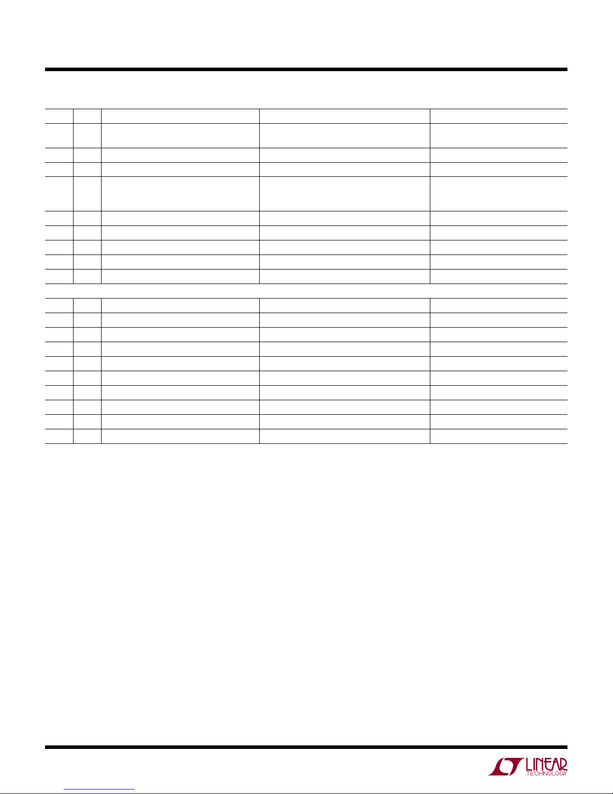
ITEM QTY REFERENCE PART DESCRIPTION MANUFACTURER/PART NUMBER
15 13 R6, R7, R8, R9, R49, R103, R111, R112,
R113, R122, R124, R137, R146
16 0 R10, R13, R14, R15 RES., OPT, 2512 OPT
17 0 R17, R108, R116, R127 RES., OPT, 1206 OPT
18 0 R25, R26, R27, R28, R30, R31, R32, R33,
R34, R35, R43, R106, R107, R119, R120,
R126, R138, R147
19 1 R77 RES., CHIP, 0, 1/8W, 0805 VISHAY, CRCW08050000Z0EA
20 1 R102 RES., CHIP, 0Ω, 1225 TEPRO,RN5326
21 1 R115 RES., CHIP, 0, 1/4W, 1206 VISHAY, CRCW12060000Z0EA
22 0 R152 RES., OPT, 0805 OPT
23 0 U3 I.C. OPT, SO16 OPT
Hardware: For Demo Board Only
1 4 E1, E2, E3, E4 TESTPOINT, TURRET, .094" MILL-MAX, 2501-2-00-80-00-00-07-0
2 3 E5, E6, E7 TESTPOINT, TURRET, .061" MILL-MAX, 2308-2-00-80-00-00-07-0
3 0 J1
4 2 J3, J4 STUD, TEST PIN PEM, KFH-032-10
5 4 J3, J4(2 EACH) NUT, BRASS, #10-32 ANY #10-32
6 2 J3, J4 WASHER, STAR #10 BRASS NICKEL ANY, #10EXT BZ TN
7 2 J3, J4 Ring, Lug Ring # 10 KEYSTONE, 8205
8 0 TP1-TP6 PAD-SMD PAD-SMD
9 4 (STAND-OFF) STAND-OFF, NYLON 0.25" KEYSTONE, 8831 (SNAP ON)
10 1 FAB, PRINTED CIRCUIT BOARD DEMO CIRCUIT 2199A
RES., CHIP, 0Ω, 0603 VISHAY, CRCW06030000Z0EA
RES., OPT, 0603 OPT
HEADER, OPT, 2×7PIN, 0.079CC
OPT, MOLEX, 87331-1420
8
dc2199aafa
Page 9
SCHEMATIC DIAGRAM
5
4
3
2
1
D
C
B
A
12
12
12
DEMO MANUAL DC2199A-A
D
DAVID B.PRODUCTION
DAVID B.PRODUCTION
DAVID B.PRODUCTION
L1
0.33
T1
LTCP26-0402T1LTCP26-0402
T3
CT02-100T3CT02-100
VIN
2512R10.33
2512
1.0uHL11.0uH
+VOUT
+VOUT
R4
R4
2512
2512
8.2K
8.2K
L3
3.3uHL33.3uH
D1
ES1PDD1ES1PD
C51
630V
C51
630V
470pF
470pF
10
92
14
8
3
34
R84
R84
1 2
C3,4,5,6
4x4.7uF
C3,4,5,6
4x4.7uF
100V
100V
L2
2.0uHL22.0uH
C2
C2
4.7uF
4.7uF
100V
100V
C1,22
C1,22
2x33uF
2x33uF
80V
80V
+
+
+VIN+VIN
REVISION HISTORY
DESCRIPTION DATEAPPROVEDECO REV
REVISION HISTORY
DESCRIPTION DATEAPPROVEDECO REV
REVISION HISTORY
DESCRIPTION DATEAPPROVEDECO REV
2 8-18-14
2 8-18-14
2 8-18-14
__
__
__
R1
12VOUT / 30A
C7,31,33,68
C7,31,33,68
4x150uF
16V
4x150uF
16V
7343
+
+
22uF
22uF
C34
16V
C34
16V
1210
BSC028N06NS3
BSC028N06NS3
Q12 BSC028N06NS3Q12 BSC028N06NS3
Q13
Q13
Q23 OPTQ23 OPT
C10
2.2nF
C10
2.2nF
1 2
R23,24
2x8.2
R23,24
2x8.2
1206
1206
FG
13
126
5
ND
0805
1.21K
1.21K
13
D27
D27
ZHCS506
ZHCS506
1210
1210
-VIN
-VIN-VIN
-VOUT
-VOUT
630V
1206
630V
1206
1206
1206
SGND PGND
BSC028N06NS3
BSC028N06NS3
Q15 BSC028N06NS3Q15 BSC028N06NS3
Q24 OPTQ24 OPT
Q14
Q14
R51,52
2x3.0
1206
R51,52
2x3.0
1206
C69
C69
630V
630V
1206
1.5nF
1.5nF
C106
150pF
250V
C106
150pF
250V
R53
6.8
1206
R53
6.8
1206
BSC190N15NS3
BSC190N15NS3
SGND
Q8 BSC190N15NS3Q8 BSC190N15NS3
Q9
Q9
0805
R76
4.22
R76
4.22
IS+
VIN
36V-60VIN
Q27
Q27
FCX491A
FCX491A
RS-
R136
0.005
R136
0.005
Q11 OPTQ11 OPT
D29
D29
13
1
215
215
R75
R75
PGNDP
1225/2512
1225/2512
R29
R29
ZHCS506
ZHCS506
C
C76
3.3nF
C76
3.3nF
1K
R421KR42
11.5K
11.5K
R41
18
17
28
21
22
24
1
2
23
3
20
28.7K
28.7K
SGND
1812
250V
250V
7
8
2
14
0805
102K
102K
12
VS+
IS+
IS-
VCC
NDRV
VIN
VAUX
SG
FG
SW
VSEC
PT+26PT-
C71
C71
T2
T2
1 6
TRANS-PA3493NL
TRANS-PA3493NL
C72
C72
C101
C101
15
IN+
IS-
IS+
PG
NDRV
VCC
3
VCP
R41
13
LTC3766EGN28
LTC3766EGN28
U2
U2
16V
16V
1uF
1uF
0805
0.1uF
0.1uF
220pF
220pF
12
+VOUT
SGND
C70
C70
3.3nF
3.3nF
IS+
C77
C77
1206
4.7uF
4.7uF
PGND
3 2
FG
0805
R114
R114
-VOUT
C30
C30
2.2nF
2.2nF
-VIN
SGNDP
100
100
R149
R149
1.5nF
1.5nF
C118
C118
100
100
R148
R148
0805
100K
100K
Q28
Q28
FDC2512
FDC2512
R18
R18
6
FB
VS-
VSOUT
ITH
SGD
FS/SYNC
MODE
IPK
PHASE
PGND
GND
REGSD
SS
RUN8FGD/SWB
25
+VOUT
0805
4
3
1.25T 1T
100
100
R101
R101
16
IN-
U1
U1
LTC3765EMSE
LTC3765EMSE
RUN
SSFLT
13
PSS
C24
C24
R46
604
R46
604
R68
R68
11
C75
C75
7
19
R69
R69
46.4K
46.4K
15
4
10
R123
R123
118K
118K
5
27
14
16
C78
C78
9
R121
R121
R118
681K
R118
681K
200V
200V
C112
0.22uF
C112
0.22uF
ND
4
AG
ISMAG
5
DELAY
6
FS/UV
PGND
1
GND
GND2
9
RCORE
11
0805
1uF
16V
1uF
16V
SGNDP
2.15K
2.15K
33nF
33nF
C73
C73
1210
C66
C66
B
SGND
C79
C79
4.7nF
4.7nF
100pF
100pF
R125
17.4K
R125
17.4K
0805
COG
133K
133K
1nF
1nF
R140
274
1/8W
R140
274
1/8W
0805
C11
C11
15nF
15nF
D34
D34
47nF
47nF
200V
200V
1206
1206
ES1PD
ES1PD
1/2W
R110
1.20
1206
R110
1.20
1206
Q29
Q29
IRF6217
IRF6217
R109
10K
R109
10K
0805
C102
0.1uF
C102
0.1uF
13
D30
D30
C80
1nF
C80
1nF
R117
12.7K
R117
12.7K
UV
R139
26.7K
R139
26.7K
10
17
14.3K
14.3K
R150
R150
C113
33nF
C113
33nF
1nF
1nF
C55
C55
SGNDP
R22
R22
3.74K
3.74K
ZHCS506
ZHCS506
100
100
R151
R151
SGNDP
1nF
1nF
C119
C119
A
www.linear.com
www.linear.com
www.linear.com
Fax: (408)434-0507
Milpitas, CA 95035
Phone: (408)432-1900
1630 McCarthy Blvd.
Fax: (408)434-0507
Milpitas, CA 95035
Phone: (408)432-1900
1630 McCarthy Blvd.
Fax: (408)434-0507
Milpitas, CA 95035
Phone: (408)432-1900
1630 McCarthy Blvd.
APPROVALS
APPROVALS
APPROVALS
CUSTOMER NOTICE
CUSTOMER NOTICE
CUSTOMER NOTICE
LINEAR TECHNOLOGY HAS MADE A BEST EFFORT TO DESIGN A
CIRCUIT THAT MEETS CUSTOMER-SUPPLIED SPECIFICATIONS;
LINEAR TECHNOLOGY HAS MADE A BEST EFFORT TO DESIGN A
CIRCUIT THAT MEETS CUSTOMER-SUPPLIED SPECIFICATIONS;
LINEAR TECHNOLOGY HAS MADE A BEST EFFORT TO DESIGN A
CIRCUIT THAT MEETS CUSTOMER-SUPPLIED SPECIFICATIONS;
NOTE:
4.7uF 100V MURATA, GRM32ER72A475KE14 (X7R 1210)
4.7uF 25V AVX, 12063C475KAT2A (X7R 1206)
22uF 16V MURATA, GRM32ER71C226MEA8L (1210 X5R)
2.2nF 250V Murata GA343QR7GD222KW01L (X7R 1812)
150uF 16V PANASONIC, 16TQC150MYF
33uF 80V PANASONIC, EEHZA1K330P (10x12.5mm)
2
2
2
SHEET OF
SHEET OF
SHEET OF
LTC Confidential-For Customer Use Only
LTC Confidential-For Customer Use Only
LTC Confidential-For Customer Use Only
ACTIVE CLAMP FORWARD CONVERTER
ACTIVE CLAMP FORWARD CONVERTER
ACTIVE CLAMP FORWARD CONVERTER
TECHNOLOGY
TECHNOLOGY
TECHNOLOGY
SCHEMATIC
SCHEMATIC
SCHEMATIC
TITLE:
TITLE:
TITLE:
LT
LT
LT
DAVID B.
DAVID B.
DAVID B.
PCB DES.
PCB DES.
PCB DES.
APP ENG.
APP ENG.
APP ENG.
HOWEVER, IT REMAINS THE CUSTOMER'S RESPONSIBILITY TO
VERIFY PROPER AND RELIABLE OPERATION IN THE ACTUAL
APPLICATION. COMPONENT SUBSTITUTION AND PRINTED
HOWEVER, IT REMAINS THE CUSTOMER'S RESPONSIBILITY TO
VERIFY PROPER AND RELIABLE OPERATION IN THE ACTUAL
APPLICATION. COMPONENT SUBSTITUTION AND PRINTED
HOWEVER, IT REMAINS THE CUSTOMER'S RESPONSIBILITY TO
VERIFY PROPER AND RELIABLE OPERATION IN THE ACTUAL
APPLICATION. COMPONENT SUBSTITUTION AND PRINTED
Unless otherwise specified:
All resistors are in ohms 0603.
L2 Vishay IHLP4040DZER2R0M11
L3 Coilcraft SER2915L-332KL
0.005 ohm Susumu KRL6432D-M-R005-F-T5 (1225)
1
DC2199A
DC2199A
DC2199A
WITH DIRECT FLUX LIMIT
WITH DIRECT FLUX LIMIT
WITH DIRECT FLUX LIMIT
LTC3765EMSE / LTC3766EGN28
LTC3765EMSE / LTC3766EGN28
LTC3765EMSE / LTC3766EGN28
Friday, October 31, 2014
Friday, October 31, 2014
Friday, October 31, 2014
IC NO. REV.
IC NO. REV.
IC NO. REV.
N/A
N/A
N/A
SIZE
DATE:
SIZE
DATE:
SIZE
DATE:
SCALE = NONE
SCALE = NONE
SCALE = NONE
2
CIRCUIT BOARD LAYOUT MAY SIGNIFICANTLY AFFECT CIRCUIT
PERFORMANCE OR RELIABILITY. CONTACT LINEAR
TECHNOLOGY APPLICATIONS ENGINEERING FOR ASSISTANCE.
THIS CIRCUIT IS PROPRIETARY TO LINEAR TECHNOLOGY AND
SUPPLIED FOR USE WITH LINEAR TECHNOLOGY PARTS.
CIRCUIT BOARD LAYOUT MAY SIGNIFICANTLY AFFECT CIRCUIT
PERFORMANCE OR RELIABILITY. CONTACT LINEAR
TECHNOLOGY APPLICATIONS ENGINEERING FOR ASSISTANCE.
THIS CIRCUIT IS PROPRIETARY TO LINEAR TECHNOLOGY AND
SUPPLIED FOR USE WITH LINEAR TECHNOLOGY PARTS.
CIRCUIT BOARD LAYOUT MAY SIGNIFICANTLY AFFECT CIRCUIT
PERFORMANCE OR RELIABILITY. CONTACT LINEAR
TECHNOLOGY APPLICATIONS ENGINEERING FOR ASSISTANCE.
THIS CIRCUIT IS PROPRIETARY TO LINEAR TECHNOLOGY AND
SUPPLIED FOR USE WITH LINEAR TECHNOLOGY PARTS.
3
4
1/4W = 1206, 1W = 2512.
All capacitors are in microfarads 0603.
All capacitors are 25V.
1/16W = 0402, 1/10W = 0603, 1/8W = 0805,
5
R110 SUSUMU, RL1632S-1R20-F (1206)
T1 Champs, LTC-PQ26-0402
T2 Pulse, PA3493NL
Simplified Schematic (without Unneeded Components)
dc2199aafa
9
Page 10
DEMO MANUAL DC2199A-A
5
4
3
2
1
D
C
B
A
12
12
12
SCHEMATIC DIAGRAM
D
DAVID B.PRODUCTION
DAVID B.PRODUCTION
DAVID B.PRODUCTION
+VOUT
+
E3+E3
8
2.0uHL22.0uH
E1
1206
1206
8.2
8.2
R3
14
+VOUT
L3
-VOUT
R24
R24
8.2 1206
8.2 1206
C51
630V
C51
630V
470pF
1206
470pF
1206
SW
PGND
OPTR3OPT
10
92
3
34
C5
C5
4.7uF
4.7uF
C4
4.7uFC4100V
4.7uF
C3
C3
4.7uF
4.7uF
C6
C6
4.7uF
4.7uF
C2
C2
4.7uF
4.7uF
C22
C22
33uF
33uF
+
+
C1
C1
33uF
33uF
+
+
36V-60VIN
3.3uHL33.3uH
Q3
312
R84
R84
100V
100V
1210
100V
1210
100V
100V
1210
100V
100V
100V
100V
80V
80V
80V
80V
J3J3
R5
OPT
R4
R4
8.2K
8.2K
CLAMP
13
126
5
OPTQ3OPT
0805
1.21K
1.21K
13
1210
1210
-VINE2-VIN
D1
R90R9
D27
D27
E2
2512R5OPT
2512
2512
2512
ES1PDD1ES1PD
FG
0
D28
D28
C23
C23
ZHCS506
ZHCS506
-VIN
REVISION HISTORY
DESCRIPTION DATEAPPROVEDECO REV
REVISION HISTORY
DESCRIPTION DATEAPPROVEDECO REV
REVISION HISTORY
DESCRIPTION DATEAPPROVEDECO REV
2 10-29-14
2 10-29-14
2 10-29-14
__
__
__
R23
R23
VA
R2
OPTR2OPT
T1
LTCP26-0402T1LTCP26-0402
OPT
2512
OPT
2512
T3
R10
R10
1 2
CT02-100T3CT02-100
VIN
R1
0.33
2512R10.33
2512
L2
L1
1.0uHL11.0uH
+VINE1+VIN
12VOUT / 30A
7343
150uF
16V
150uF
16V
C68
C68
+
+
OPT
OPT
C26+C26
C25+C25
+
+
+
+
C7
C7
150uF
16V
150uF
16V
7343
+
+
16V
16V
C31
150uF
C31
150uF
7343
+
+
C33
150uF
16V+C33
150uF
16V
7343
+
22uF
22uF
C34
16V
C34
16V
1210
OPT
OPT
BSC028N06NS3
BSC028N06NS3
Q23
Q23
Q12 BSC028N06NS3Q12 BSC028N06NS3
Q13
Q13
4
4
4
5
5
5
678
678
678
C10
2.2nF
630V
C10
2.2nF
630V
1 2
FG
4
4
4
5
5
5
678
678
678
SWB
C69
C69
1206
630V
630V
1.5nF
1.5nF
C106
C106
R53
6.8
1206
R53
6.8
1206
6 7 8
6 7 8
6 7 8
5
5
5
ND
SGND
13
0805
OPT
OPT
R76
4.22
R76
4.22
IS+
-VOUT
1
1
1
23
23
23
1206
1206
RS+RS-
R102
R102
1
1
1
23
23
23
R52
3.0
R52
3.0
R51
3.0
R51
3.0
150pF
200V
150pF
200V
4
4
4
R490R49
VIN
J4J4
0
0
Q15 BSC028N06NS3Q15 BSC028N06NS3
1206
1206
1206
1206
2 3
2 3
2 3
1
1
1
BSC190N15NS3
BSC190N15NS3
Q8 BSC190N15NS3Q8 BSC190N15NS3
Q9
Q9
0
-
E4-E4
-VOUT
VCC
RS+RS-
R7
0
R7
0
VPK
R147
R147
RUN
0
0
R6
0603
R6
0603
0
R1030R103
215
215
0805
R75
R75
1225
1225
OPT
OPT
BSC028N06NS3
BSC028N06NS3
Q24
Q24
Q14
Q14
RS-
R136
0.005
R136
0.005
Q11 OPTQ11 OPT
ZHCS506
ZHCS506
D29
D29
13
VS+
0603
0603
R1370R137
OPT
OPT
C111
C111
C8
OPTC8OPT
R770R77
SGND PGND
PGNDP
1225/2512
1225/2512
R29
R29
+SENSE
E5E5
OPT
OPT
R126
R126
OPT
OPT
R107
R107
R106
R106
Q27
Q27
0
100
100
R148
R148
100K
100K
OPT
OPT
0
0805
R108
R108
C
VS-
FCX491A
FCX491A
OPT
OPT
PGND
C30
C30
SGNDP
R149
R149
0805
Q28
Q28
2
5
6
-SENSE
IS+
C103
C103
1
1206
OPT
OPT
2.2nF
2.2nF
100
100
C118
C118
FDC2512
FDC2512
B
C76
3.3nF
C76
3.3nF
1K
R421KR42
11.5K
11.5K
R41
SGND
3.3nF
3.3nF
OPT
OPT
R1130R113
OPT
OPT
VAUX
0
R1120R112
0
R1110R111
0
R1460R146
R114
R114
1812
250V
250V
7
8
2
14
4 1
0805
R11501/4W
R11501/4W
12
IS+
18
IS-
17
0
28
1206
1206
21
VIN
22
24
SG
1
FG
2
SW
23
3
20
28.7K
28.7K
SGND
C71
1uF
C71
1uF
T2
T2
1 6
TRANS-PA3493NL
TRANS-PA3493NL
C72
C72
0.1uF
0.1uF
C101
C101
15
IN+
IS-
IS+
PG
NDRV
VCC
3
VCP
D40
D40
1 2
E7E7
RUN
R41
C740C74
0
1206
13
VS+
VCC
NDRV
VAUX
LTC3766EGN
LTC3766EGN
U2
U2
VSEC
PT+26PT-
16V
16V
0805
4
3
1.25T 1T
0805
R101
R101
220pF
220pF
U1
U1
RUN
12
PSS
1N4148WS
1N4148WS
6
FB
VS-
VSOUT
ITH
SGD
FS/SYNC
MODE
IPK
PHASE
PGND
GND
REGSD
SS
RUN8FGD/SWB
25
PT-
C112
C112
ND
AG
100
100
AG
4
16
IN-
AG
LTC3765EMSE
LTC3765EMSE
SSFLT
RCORE
13
11
0805
C24
1uF
16V
C24
1uF
16V
E6E6
+VOUT
C70
C70
VCC
3 2
R116
R116
R138
OPT
R138
OPT
FG
-VOUT
-VIN
1.5nF
1.5nF
3
R18
102K
R18
102K
R119
R119
11
7
19
15
4
10
5
27
14
16
9
0.22uF
0.22uF
SGNDP
R80R8
ISMAG
DELAY
FS/UV
PGND
GND
GND2
C9
OPTC9OPT
SGND
R46
604
R46
604
1206
R127
OPT
1/4W
R127
OPT
1/4W
1206
C77
C77
4.7uF
4.7uF
PGND
VCC
OPT
OPT
R120
R120
OPT
OPT
C79
C79
4.7nF
4.7nF
R68
2.15K
R68
2.15K
C75
C75
ITH-
100pF
100pF
R125
17.4K
R125
17.4K
SYNC ITH
R69
R69
46.4K
46.4K
R43
OPT
R43
OPT
VCC
R1240R124
0
0
R123
R123
118K
118K
R1220R122
0
C1050C105
C78
C78
33nF
33nF
0805
SSS
RUN
+VOUT
1210
200V
200V
C66
47nF
C66
47nF
0
5
6
10
1
17
9
COG
R121
133K
R121
133K
1nF
1nF
C73
C73
R118
681K
R118
681K
0805
R140
274
1/8W
R140
274
1/8W
C11
C11
15nF
15nF
D34
D34
ES1PD
ES1PD
200V
200V
1206
1206
3
8
2
7
6
5
Q29
Q29
IRF6217
IRF6217
AG1
C102
0.1uF
C102
0.1uF
AG1
C80
1nF
C80
1nF
AS
R117
12.7K
R117
12.7K
UV
R139
26.7K
R139
26.7K
14.3K
14.3K
R150
R150
C113
33nF
C113
33nF
1nF
1nF
C55
C55
R22
R22
3.74K
3.74K
0805
1
4
1
32
13
SGNDP
1/2W
R110
1.20
1206
R110
1.20
1206
Q31
Q31
OPT
OPT
100
100
R151
R151
R109
10K
R109
10K
AS
D30
D30
ZHCS506
ZHCS506
C119
C119
SGNDP
1nF
1nF
A
www.linear.com
www.linear.com
www.linear.com
Fax: (408)434-0507
Milpitas, CA 95035
Phone: (408)432-1900
1630 McCarthy Blvd.
Fax: (408)434-0507
Milpitas, CA 95035
Phone: (408)432-1900
1630 McCarthy Blvd.
Fax: (408)434-0507
Milpitas, CA 95035
Phone: (408)432-1900
1630 McCarthy Blvd.
APPROVALS
APPROVALS
APPROVALS
CUSTOMER NOTICE
CUSTOMER NOTICE
CUSTOMER NOTICE
LINEAR TECHNOLOGY HAS MADE A BEST EFFORT TO DESIGN A
CIRCUIT THAT MEETS CUSTOMER-SUPPLIED SPECIFICATIONS;
LINEAR TECHNOLOGY HAS MADE A BEST EFFORT TO DESIGN A
CIRCUIT THAT MEETS CUSTOMER-SUPPLIED SPECIFICATIONS;
LINEAR TECHNOLOGY HAS MADE A BEST EFFORT TO DESIGN A
CIRCUIT THAT MEETS CUSTOMER-SUPPLIED SPECIFICATIONS;
2
2
2
SHEET OF
SHEET OF
SHEET OF
LTC Confidential-For Customer Use Only
LTC Confidential-For Customer Use Only
LTC Confidential-For Customer Use Only
TECHNOLOGY
TECHNOLOGY
TECHNOLOGY
SCHEMATIC
SCHEMATIC
SCHEMATIC
TITLE:
TITLE:
TITLE:
LT
LT
LT
DAVID B.
DAVID B.
DAVID B.
PCB DES.
PCB DES.
PCB DES.
APP ENG.
APP ENG.
APP ENG.
HOWEVER, IT REMAINS THE CUSTOMER'S RESPONSIBILITY TO
VERIFY PROPER AND RELIABLE OPERATION IN THE ACTUAL
APPLICATION. COMPONENT SUBSTITUTION AND PRINTED
HOWEVER, IT REMAINS THE CUSTOMER'S RESPONSIBILITY TO
VERIFY PROPER AND RELIABLE OPERATION IN THE ACTUAL
APPLICATION. COMPONENT SUBSTITUTION AND PRINTED
HOWEVER, IT REMAINS THE CUSTOMER'S RESPONSIBILITY TO
VERIFY PROPER AND RELIABLE OPERATION IN THE ACTUAL
APPLICATION. COMPONENT SUBSTITUTION AND PRINTED
1
DC2199A
DC2199A
DC2199A
WITH DIRECT FLUX LIMIT
WITH DIRECT FLUX LIMIT
WITH DIRECT FLUX LIMIT
ACTIVE CLAMP FORWARD CONVERTER
ACTIVE CLAMP FORWARD CONVERTER
ACTIVE CLAMP FORWARD CONVERTER
LTC3765EMSE / LTC3766EGN
LTC3765EMSE / LTC3766EGN
LTC3765EMSE / LTC3766EGN
Wednesday, October 29, 2014
Wednesday, October 29, 2014
Wednesday, October 29, 2014
IC NO. REV.
IC NO. REV.
IC NO. REV.
N/A
N/A
N/A
SIZE
DATE:
SIZE
DATE:
SIZE
DATE:
SCALE = NONE
SCALE = NONE
SCALE = NONE
2
CIRCUIT BOARD LAYOUT MAY SIGNIFICANTLY AFFECT CIRCUIT
PERFORMANCE OR RELIABILITY. CONTACT LINEAR
TECHNOLOGY APPLICATIONS ENGINEERING FOR ASSISTANCE.
THIS CIRCUIT IS PROPRIETARY TO LINEAR TECHNOLOGY AND
SUPPLIED FOR USE WITH LINEAR TECHNOLOGY PARTS.
CIRCUIT BOARD LAYOUT MAY SIGNIFICANTLY AFFECT CIRCUIT
PERFORMANCE OR RELIABILITY. CONTACT LINEAR
TECHNOLOGY APPLICATIONS ENGINEERING FOR ASSISTANCE.
THIS CIRCUIT IS PROPRIETARY TO LINEAR TECHNOLOGY AND
SUPPLIED FOR USE WITH LINEAR TECHNOLOGY PARTS.
CIRCUIT BOARD LAYOUT MAY SIGNIFICANTLY AFFECT CIRCUIT
PERFORMANCE OR RELIABILITY. CONTACT LINEAR
TECHNOLOGY APPLICATIONS ENGINEERING FOR ASSISTANCE.
THIS CIRCUIT IS PROPRIETARY TO LINEAR TECHNOLOGY AND
SUPPLIED FOR USE WITH LINEAR TECHNOLOGY PARTS.
3
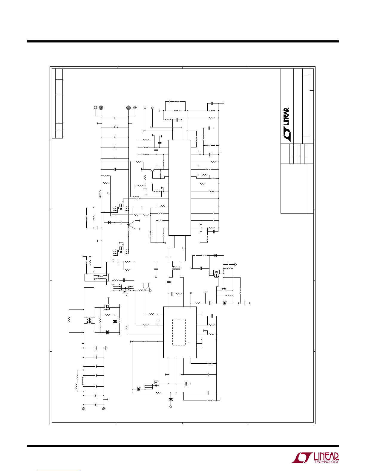
Full Schematic, Page 1
4
1/4W = 1206, 1W = 2512.
Unless otherwise specified:
All resistors are in ohms 0603.
All capacitors are in microfarads 0603.
All capacitors are 25V.
1/16W = 0402, 1/10W = 0603, 1/8W = 0805,
5
NOTE:
4.7uF 100V MURATA, GRM32ER72A475KE14 (X7R 1210)
4.7uF 25V AVX, 12063C475KAT2A (X7R 1206)
22uF 16V MURATA, GRM32ER71C226MEA8L (1210 X5R)
2.2nF 250V Murata GA343QR7GD222KW01L (X7R 1812)
150uF 16V PANASONIC, 16TQC150MYF
33uF 80V PANASONIC, EEHZA1K330P (10x12.5mm)
L2 Vishay IHLP4040DZER2R0M11
L3 Coilcraft SER2915L-332KL
0.005 ohm Susumu KRL6432D-M-R005-F-T5 (1225)
R110 SUSUMU, RL1632S-1R20-F (1206)
T1 Champs, LTC-PQ26-0402
T2 Pulse, PA3493NL
10
dc2199aafa
Page 11

SCHEMATIC DIAGRAM
5
4
3
2
1
D
C
B
A
22
22
22
DEMO MANUAL DC2199A-A
D
4
R34
OPT
R34
OPT
PSSPSS
PSS
CLAMP
R15
6.8
2512
R15
6.8
2512
R17
1206
R17
1206
100K
100K
R14
6.8
2512
R14
6.8
2512
15nF
200V
1206
15nF
200V
1206
R13
6.8
2512
R13
6.8
2512
RS-
C20
0.1uF
C20
0.1uF
VCC
ACTIVE SNUBBER
16
5
U3
U3
SO16
SO16
3
HEF4528BT
HEF4528BT
4
1.00K
1.00K
C12
47pF
C12
47pF
5
776
5
6
R26 OPTR26 OPT
SGND
Q4
C15
C15
0.1uF
0805
0.1uF
0805
4
Q1
2
5
C14
C14
0.1uF
0.1uF
7
VDD
Q1
B1
RES
A1
CRX
2
C13
C13
R12
4.99K
R12
4.99K
1122334
J1
R25
OPT
R25
OPT
SGNDPSGNDP
SGNDP
C17
C17
SWFG
OPTIONAL CIRCUITS
R11
R11
8
R35 OPTR35 OPT
SSSSSS
FQD4P25Q4FQD4P25
R19
1.5K
R19
1.5K
D2
316
C16
C16
VSS2
VSS1
VSS
10pF
10pF
8
SSS
1 2
OPTD2OPT
ZXGD3002E6Q1ZXGD3002E6
56pF
56pF
15
8
1
C
141413131212111110109
9
R28 OPTR28 OPT
R27 OPTR27 OPT
R32 OPTR32 OPT
ITHITH
PT-PT-
VS+VS+
ITH
VS+
R30 OPTR30 OPT
R31 OPTR31 OPT
VS-VS-
ITH-ITH-
VS-
ITH-
RS-
OPTJ1OPT
HD2X7-MOLEX
R33 OPTR33 OPT
SYNCSYNC
PT-
SYNC
B
VPK
C114
C114
R152
R152
OPT
OPT
12
D35
D35
OPT
OPT
PEAK CHARGE VCC
VA
OPT
OPT
C116
C116
VAUX
L4
OPTL4OPT
D38
D38
D37
OPT
D37
OPT
VCC FROM T1
1 3
VA
VA
C21
OPT
0805
C21
OPT
0805
SW
12
D4
+VOUT
PGNDP
C19
C19
OPT
OPT
VCCP
Q2
OPTQ2OPT
2
AC DRIVER
AG AG1
A
www.linear.com
www.linear.com
www.linear.com
Fax: (408)434-0507
Milpitas, CA 95035
Phone: (408)432-1900
1630 McCarthy Blvd.
Fax: (408)434-0507
Milpitas, CA 95035
Phone: (408)432-1900
1630 McCarthy Blvd.
Fax: (408)434-0507
Milpitas, CA 95035
Phone: (408)432-1900
1630 McCarthy Blvd.
PGNDPGND
OPT
0805
OPT
0805
APPROVALS
APPROVALS
0805
0805
1206
1206
OPT
OPT
1 3
OPTD4OPT
APPROVALS
CUSTOMER NOTICE
CUSTOMER NOTICE
CUSTOMER NOTICE
LINEAR TECHNOLOGY HAS MADE A BEST EFFORT TO DESIGN A
CIRCUIT THAT MEETS CUSTOMER-SUPPLIED SPECIFICATIONS;
LINEAR TECHNOLOGY HAS MADE A BEST EFFORT TO DESIGN A
CIRCUIT THAT MEETS CUSTOMER-SUPPLIED SPECIFICATIONS;
LINEAR TECHNOLOGY HAS MADE A BEST EFFORT TO DESIGN A
CIRCUIT THAT MEETS CUSTOMER-SUPPLIED SPECIFICATIONS;
2
2
2
SHEET OF
SHEET OF
SHEET OF
LTC Confidential-For Customer Use Only
LTC Confidential-For Customer Use Only
LTC Confidential-For Customer Use Only
ACTIVE CLAMP FORWARD CONVERTER
ACTIVE CLAMP FORWARD CONVERTER
ACTIVE CLAMP FORWARD CONVERTER
TECHNOLOGY
TECHNOLOGY
TECHNOLOGY
SCHEMATIC
SCHEMATIC
SCHEMATIC
TITLE:
TITLE:
TITLE:
LT
LT
LT
DAVID B.
DAVID B.
DAVID B.
PCB DES.
PCB DES.
PCB DES.
APP ENG.
APP ENG.
APP ENG.
HOWEVER, IT REMAINS THE CUSTOMER'S RESPONSIBILITY TO
VERIFY PROPER AND RELIABLE OPERATION IN THE ACTUAL
APPLICATION. COMPONENT SUBSTITUTION AND PRINTED
HOWEVER, IT REMAINS THE CUSTOMER'S RESPONSIBILITY TO
VERIFY PROPER AND RELIABLE OPERATION IN THE ACTUAL
APPLICATION. COMPONENT SUBSTITUTION AND PRINTED
HOWEVER, IT REMAINS THE CUSTOMER'S RESPONSIBILITY TO
VERIFY PROPER AND RELIABLE OPERATION IN THE ACTUAL
APPLICATION. COMPONENT SUBSTITUTION AND PRINTED
1
DC2199A
DC2199A
DC2199A
WITH DIRECT FLUX LIMIT
WITH DIRECT FLUX LIMIT
WITH DIRECT FLUX LIMIT
LTC3765EMSE / LTC3766EGN
LTC3765EMSE / LTC3766EGN
LTC3765EMSE / LTC3766EGN
Wednesday, October 29, 2014
Wednesday, October 29, 2014
Wednesday, October 29, 2014
IC NO. REV.
IC NO. REV.
IC NO. REV.
N/A
N/A
N/A
SIZE
DATE:
SIZE
DATE:
SIZE
DATE:
SCALE = NONE
SCALE = NONE
SCALE = NONE
2
CIRCUIT BOARD LAYOUT MAY SIGNIFICANTLY AFFECT CIRCUIT
PERFORMANCE OR RELIABILITY. CONTACT LINEAR
TECHNOLOGY APPLICATIONS ENGINEERING FOR ASSISTANCE.
THIS CIRCUIT IS PROPRIETARY TO LINEAR TECHNOLOGY AND
SUPPLIED FOR USE WITH LINEAR TECHNOLOGY PARTS.
CIRCUIT BOARD LAYOUT MAY SIGNIFICANTLY AFFECT CIRCUIT
PERFORMANCE OR RELIABILITY. CONTACT LINEAR
TECHNOLOGY APPLICATIONS ENGINEERING FOR ASSISTANCE.
THIS CIRCUIT IS PROPRIETARY TO LINEAR TECHNOLOGY AND
SUPPLIED FOR USE WITH LINEAR TECHNOLOGY PARTS.
CIRCUIT BOARD LAYOUT MAY SIGNIFICANTLY AFFECT CIRCUIT
PERFORMANCE OR RELIABILITY. CONTACT LINEAR
TECHNOLOGY APPLICATIONS ENGINEERING FOR ASSISTANCE.
THIS CIRCUIT IS PROPRIETARY TO LINEAR TECHNOLOGY AND
SUPPLIED FOR USE WITH LINEAR TECHNOLOGY PARTS.
3
Full Schematic, page 2
4
316
4
PGNDP
5
C18
OPT
C18
OPT
PGNDP
AG AG1
Information furnished by Linear Technology Corporation is believed to be accurate and reliable.
However, no responsibility is assumed for its use. Linear Technology Corporation makes no representation that the interconnection of its circuits as described herein will not infringe on existing patent rights.
5
dc2199aafa
11
Page 12

DEMO MANUAL DC2199A-A
DEMONSTRATION BOARD IMPORTANT NOTICE
Linear Technology Corporation (LT C ) provides the enclosed product(s) under the following AS IS conditions:
This demonstration board (DEMO BOARD) kit being sold or provided by Linear Technology is intended for use for ENGINEERING DEVELOPMENT
OR EVALUATION PURPOSES ONLY and is not provided by LTC for commercial use. As such, the DEMO BOARD herein may not be complete
in terms of required design-, marketing-, and/or manufacturing-related protective considerations, including but not limited to product safety
measures typically found in finished commercial goods. As a prototype, this product does not fall within the scope of the European Union
directive on electromagnetic compatibility and therefore may or may not meet the technical requirements of the directive, or other regulations.
If this evaluation kit does not meet the specifications recited in the DEMO BOARD manual the kit may be returned within 30 days from the date
of delivery for a full refund. THE FOREGOING WARRANTY IS THE EXCLUSIVE WARRANTY MADE BY THE SELLER TO BUYER AND IS IN LIEU
OF ALL OTHER WARRANTIES, EXPRESSED, IMPLIED, OR STATUTORY, INCLUDING ANY WARRANTY OF MERCHANTABILITY OR FITNESS
FOR ANY PARTICULAR PURPOSE. EXCEPT TO THE EXTENT OF THIS INDEMNITY, NEITHER PARTY SHALL BE LIABLE TO THE OTHER FOR
ANY INDIRECT, SPECIAL, INCIDENTAL, OR CONSEQUENTIAL DAMAGES.
The user assumes all responsibility and liability for proper and safe handling of the goods. Further, the user releases LT C from all claims
arising from the handling or use of the goods. Due to the open construction of the product, it is the user’s responsibility to take any and all
appropriate precautions with regard to electrostatic discharge. Also be aware that the products herein may not be regulatory compliant or
agency certified (FCC, UL, CE, etc.).
No License is granted under any patent right or other intellectual property whatsoever. LT C assumes no liability for applications assistance,
customer product design, software performance, or infringement of patents or any other intellectual property rights of any kind.
LT C currently services a variety of customers for products around the world, and therefore this transaction is not exclusive.
Please read the DEMO BOARD manual prior to handling the product. Persons handling this product must have electronics training and
observe good laboratory practice standards. Common sense is encouraged.
This notice contains important safety information about temperatures and voltages. For further safety concerns, please contact a LT C application engineer.
Mailing Address:
Linear Technology
1630 McCarthy Blvd.
Milpitas, CA 95035
Copyright © 2004, Linear Technology Corporation
Linear Technology Corporation
12
1630 McCarthy Blvd., Milpitas, CA 95035-7417
(408) 432-1900 ● FAX: (408) 434-0507 ● www.linear.com
dc2199aafa
LT 1114 REV A • PRINTED IN USA
LINEAR TECHNOLOGY CORPORATION 2014
 Loading...