

Page 1
LTC3576/LTC3576-1
Switching Power Manager
with USB On-the-Go + Triple
Step-Down DC/DCs
FEATURES
n
Bidirectional Switching Regulator with Bat-
Track™ Adaptive Output Control Provides Effi cient
Charging and
n
Bat-Track Control of External High Voltage Step-
a 5V Output for USB On-The-Go
Down Switching Regulator
n
Overvoltage Protection Guards Against Damage
n
“Instant-On” Operation with Discharged Battery
n
Triple Step-Down Switching Regulators with I2C
Adjustable Outputs (1A/400mA/400mA I
n
180mΩ Internal Ideal Diode + External Ideal Diode
OUT
)
Controller Powers the Load in Battery Mode
n
Li-Ion/Polymer Battery Charger (1.5A Max I
n
Battery Float Voltage: 4.2V (LTC3576), 4.1V (LTC3576-1)
n
Compact (4mm × 6mm × 0.75mm) 38-pin QFN Package
CHG
)
APPLICATIONS
n
HDD-Based Media Players
n
GPS, PDAs, Digital Cameras, Smart Phones
n
Automotive Compatible Portable Electronics
DESCRIPTION
The LTC
management and battery charger ICs for Li-Ion/Polymer
battery applications. They each include a high effi ciency,
bidirectional switching PowerPath™ manager with automatic load prioritization, a battery charger, an ideal diode, a
controller for an external high voltage switching regulator
and three general purpose step-down switching regulators
with I
ing regulators automatically limit input current for USB
compatibility and can also generate 5V at 500mA for USB
on-the-go applications when powered from the battery.
Both the USB and external switching regulator power paths
feature Bat-Track optimized charging to provide maximum
power to the application from supplies as high as 38V. An
overvoltage circuit protects the LTC3576/LTC3576-1 from
damage due to high voltage on the V
just two external components. The LTC3576/LTC3576-1 are
available in a low profi le 38-pin (4mm × 6mm × 0.75mm)
QFN package.
L, LT, LTC and LTM are registered trademarks of Linear Technology Corporation. Bat-Track
and PowerPath are trademarks of Linear Technology Corporation. All other trademarks are the
property of their respective owners. Protected by U.S. Patents, including 6522118, 6404251.
®
3576/LTC3576-1 are highly integrated power
2
C adjustable output voltages. The internal switch-
or WALL pins with
BUS
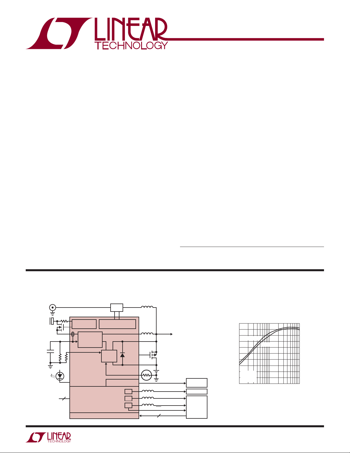
TYPICAL APPLICATION
High Effi ciency PowerPath Manager with Overvoltage Protection
and Triple Step-Down Regulator
AUTOMOTIVE
FIREWIRE, ETC.
USB OR
5V AC
ADAPTER
CONTROLS
ENABLE
CHARGE
6
OVERVOLTAGE
PROTECTION
USB COMPLIANT
BIDIRECTIONAL
SWITCHING
REGULATOR
LTC3576/LTC3576-1
HIGH EFFICIENCY
LT3653
EXTERNAL HIGH VOLTAGE
BUCK CONTROLLER
CC/CV
BATTERY
CHARGER
ALWAYS ON LDO
TRIPLE
STEP-DOWN
SWITCHING
REGULATORS
2
C PORT
I
0V
T
1
2
3
OPTIONAL
+
Li-Ion
3.3V/20mA
0.8V TO 3.6V/400mA
0.8V TO 3.6V/400mA
0.8V TO 3.6V/1A
RST
2
TO OTHER
LOADS
RTC/LOW
POWER LOGIC
MEMORY
I/O
CORE
µPROCESSOR
2
C
I
3576 TA01
PowerPath Switching Regulator Effi ciency
to System Load (P
100
90
80
BAT = 4.2V
70
60
50
40
EFFICIENCY (%)
30
20
V
BUS
I
BAT
10
10x MODE
0
10
= 5V
= 0mA
LOAD CURRENT (mA)
BAT = 3.3V
VOUT/PVBUS
100 1000
)
3576 TA01b
3576f
1
Page 2
LTC3576/LTC3576-1
(Notes 1, 2, 3)
V
, WALL (Transient) t < 1ms,
BUS
Duty Cycle < 1% .......................................... –0.3V to 7V
, WALL (Static), BAT, V
V
BUS
, ENOTG, NTC, SDA, SCL, DVCC,
V
OUT
RST3, CHRG ................................................ –0.3V to 6V
, I
I
LIM0
.........–0.3V to Max(V
ILIM1
EN1, EN2, EN3 ...............................–0.3V to V
FBx (x = 1, 2, 3) ..............................–0.3V to V
I
OVSENS
I
CLPROG
I
CHRG
I
PROG
I
LDO3V3
I
SW1
I
SW
...................................................................10mA
....................................................................3mA
, I
............................................................50mA
RST3
........................................................................2mA
...................................................................30mA
, I
(Continuous) .......................................600mA
SW2
, I
, I
SW3
BAT
, I
(Continuous) ..............................2A
VOUT
Maximum Junction Temperature........................... 125°C
Operating Temperature Range.................. –40°C to 85°C
Storage Temperature Range ................... –65°C to 125°C
IN1
, V
IN2
BUS
, V
,
IN3
, V
, BAT) + 0.3V
OUT
OUT
INx
+ 0.3V
+ 0.3V
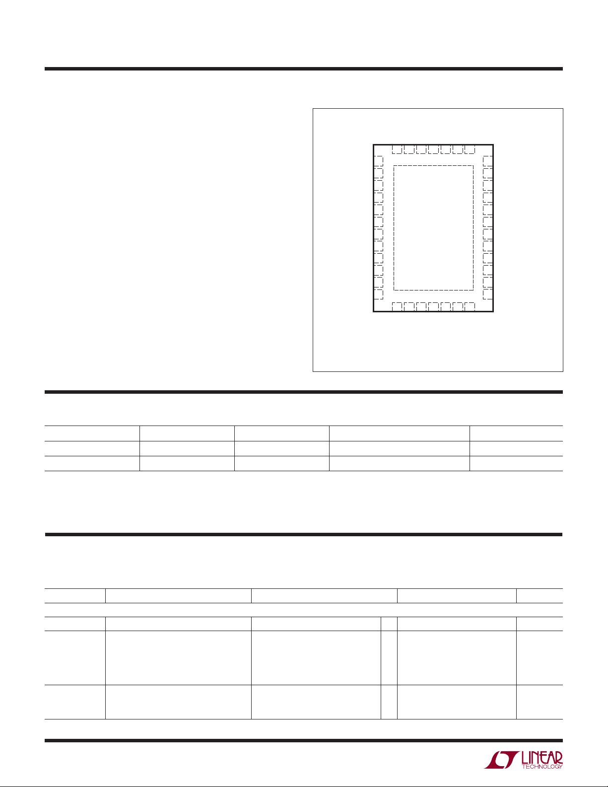
PIN CONFIGURATION ABSOLUTE MAXIMUM RATINGS
TOP VIEW
LIM1ILIM0
I
38 37 36 35 34 33 32
1CLPROG
LDO3V3
2
NTCBIAS
3
NTC
4
OVGATE
5
OVSENS
6
FB1
7
V
8
IN1
SW1
9
EN1
10
ENOTG
11
DV
12
CC
13 14 15 16
SCL
38-LEAD (4mm s 6mm) PLASTIC QFN
T
EXPOSED PAD (PIN 39) IS GND, MUST BE SOLDERED TO PCB
JMAX
BUSVBUSVOUT
SW
V
39
17 18 19
NC
SDA
UFE PACKAGE
= 125°C, θJA = 34°C/W
NC
IN3
V
SW3
BAT
EN3
31
30
29
28
27
26
25
24
23
22
21
20
IDGATE
CHRG
PROG
ACPR
WALL
V
C
FB2
V
IN2
SW2
EN2
RST3
FB3
ORDER INFORMATION
LEAD FREE FINISH TAPE AND REEL PART MARKING PACKAGE DESCRIPTION TEMPERATURE RANGE
LTC3576EUFE#PBF LTC3576EUFE#TRPBF 3576
LTC3576EUFE-1#PBF LTC3576EUFE-1#TRPBF 35761
Consult LTC Marketing for parts specifi ed with wider operating temperature ranges.
Consult LTC Marketing for information on non-standard lead based fi nish parts.
For more information on lead free part marking, go to: http://www.linear.com/leadfree/
For more information on tape and reel specifi cations, go to: http://www.linear.com/tapeandreel/
ELECTRICAL CHARACTERISTICS
The l denotes the specifi cations which apply over the full operating
temperature range, otherwise specifi cations are at TA = 25°C. V
BUS
38-Lead (4mm × 6mm) Plastic QFN
38-Lead (4mm × 6mm) Plastic QFN
= 5V, BAT = 3.8V, DVCC = 3.3V, R
CLPROG
otherwise noted.
SYMBOL PARAMETER CONDITIONS MIN TYP MAX UNITS
PowerPath Switching Regulator—Step-Down Mode
V
BUS
I
VBUS(LIM)
I
(Note 4) Input Quiescent Current
VBUSQ
Input Supply Voltage 4.35 5.5 V
Total Input Current
1× Mode
5× Mode
10× Mode
Low Power Suspend Mode
High Power Suspend Mode
1× Mode
5×, 10× Modes
Low/High Power Suspend Modes
l
82
l
440
l
800
l
0.32
l
1.6
–40°C to 85°C
–40°C to 85°C
= 3.01k, unless
90
472
880
0.39
2.05
7
17
0.045
100
500
1000
0.5
2.5
mA
mA
mA
mA
mA
mA
mA
mA
2
3576f
Page 3

LTC3576/LTC3576-1
ELECTRICAL CHARACTERISTICS
The l denotes the specifi cations which apply over the full operating
temperature range, otherwise specifi cations are at T
= 25°C. V
A
otherwise noted.
SYMBOL PARAMETER CONDITIONS MIN TYP MAX UNITS
h
CLPROG
(Note 4)
I
VOUT(POWERPATH)VOUT
V
CLPROG
V
UVLO
V
DUVLO
V
V
OUT
f
OSC
R
PMOS_
POWERPATH
R
NMOS_
POWERPATH
I
PEAK_POWERPATH
R
SUSP
PowerPath Switching Regulator—Step-Up Mode (USB On-the-Go)
V
BUS
V
OUT
I
VBUS
I
PEAK
I
OTGQ
V
CLPROG
V
OUT(UVLO)
t
SCFAULT
Bat-Track Switching Regulator Control
V
WALL
ΔV
WALL
V
OUT
I
WALLQ
R
ACPR
V
HACPR
V
LACPR
Ratio of Measured V
CLPROG Program Current
Current to
BUS
1x Mode
5x Mode
10x Mode
Low Power Suspend Mode
High Power Suspend Mode
Current Available Before
Discharging Battery
1x Mode, BAT = 3.3V
5x Mode, BAT = 3.3V
10x Mode, BAT = 3.3V
Low Power Suspend Mode
High Power Suspend Mode
CLPROG Servo Voltage in Current Limit Switching Modes
Suspend Modes
V
Undervoltage Lockout Rising Threshold
BUS
Falling Threshold 3.95
V
to BAT Differential Undervoltage
BUS
Lockout
Voltage 1x, 5x, 10x Modes, 0V < BAT < 4.2V,
OUT
Rising Threshold
Falling Threshold
I
VOUT
USB Suspend Modes, I
Switching Frequency 1.8 2.25 2.7 MHz
PMOS On-Resistance 0.18
NMOS On-Resistance 0.30
Peak Inductor Current Limit 1x Mode (Note 5)
5x Mode (Note 5)
10x Mode (Note 5)
Suspend LDO Output Resistance Closed Loop 10
Output Voltage 0mA ≤ I
Input Voltage 2.9 5.5 V
Output Current Limit
V
Leakage Current in Shutdown On-the-Go Disabled, V
BUS
Peak Inductor Current Limit (Note 5) 1.8 A
V
Quiescent Current V
OUT
OUT
= 3.8V, I
Output Current Limit Servo Voltage 1.15 V
V
UVLO—V
OUT
V
UVLO—V
OUT
Short-Circuit Fault Delay V
OUT
OUT
Falling
Rising
< 4V and PMOS Switch Off 7.2 ms
BUS
Absolute WALL Input Threshold Rising Threshold
Hysteresis
Differential WALL Input Threshold WALL-BAT Falling
Hysteresis
Regulation Target Under VC Control 3.55 BAT + 0.3 V
WALL Quiescent Current 100 µA
ACPR Pull-Down Strength 100
ACPR High Voltage V
ACPR Low Voltage 0V
= 5V, BAT = 3.8V, DVCC = 3.3V, R
BUS
= 0mA, Battery Charger Off
= 250µA
VOUT
≤ 500mA, V
VBUS
VBUS
= 0mA (Note 6) 1.38 mA
> 3.2V 4.75 5.25 V
OUT
< UVLO
BUS
= 3.01k, unless
CLPROG
210
1160
2200
9.6
56
121
667
1217
0.26
1.6
0.31
2
0.41
2.4
1.18
100
4.30
4.35 V
4.00
200
50
3.4
4.5
BAT + 0.3
4.6
4.7
4.7
1
2
3
l
550
–150
680
0 150
2.5 2.6
2.8 2.9
4.2 4.3
4.4 V
1.1
0306045 mV
OUT
mA/mA
mA/mA
mA/mA
mA/mA
mA/mA
mA
mA
mA
mA
mA
mV
mV
mV
mA
nA
mV
3576f
V
V
V
V
A
A
A
V
V
V
V
3
Page 4

LTC3576/LTC3576-1
ELECTRICAL CHARACTERISTICS
The l denotes the specifi cations which apply over the full operating
temperature range, otherwise specifi cations are at T
= 25°C. V
A
otherwise noted.
SYMBOL PARAMETER CONDITIONS MIN TYP MAX UNITS
Overvoltage Protection
V
OVCUTOFF
V
OVGATE
t
RISE
Battery Charger
V
FLOAT
I
CHG
I
BAT
V
PROG
V
PROG_TRKL
V
C/10
h
PROG
I
TRKL
V
TRKL
ΔV
TRKL
ΔV
RECHRG
t
TERM
t
BADBAT
h
C/10
V
CHRG
I
CHRG
R
ON_CHG
T
LIM
NTC
V
COLD
Overvoltage Protection Threshold With 6.2k Series Resistor 6.1 6.35 6.7 V
OVGATE Output Voltage V
OVSENS
V
OVSENS
OVGATE Time to Reach Regulation OVGATE C
BAT Regulated Output Voltage LTC3576
LTC3576-1
Constant Current Mode Charger Current R
Battery Drain Current V
PROG
R
PROG
BUS
I
VOUT
V
BUS
> V
= 0µA
= 0V, I
(Ideal Diode Mode)
PROG Pin Servo Voltage 1.000 V
PROG Pin Servo Voltage in Trickle Charge BAT < V
C/10 Threshold Voltage at PROG 100 mV
Ratio of I
to PROG Pin Current 1030 mA/mA
BAT
Trickle Charge Current BAT < V
Trickle Charge Threshold Voltage BAT Rising 2.7 2.85 3.0 V
Trickle Charge Hysteresis Voltage 135 mV
Recharge Battery Threshold Voltage Threshold Voltage Relative to V
Safety Timer Termination Period Timer Starts When V
Bad Battery Termination Time BAT < V
End of Charge Current Ratio (Note 7) 0.085 0.1 0.112 mA/mA
CHRG Pin Output Low Voltage I
CHRG Pin Leakage Current V
= 5mA 65 100 mV
CHRG
CHRG
Battery Charger Power FET OnResistance (Between V
and BAT)
OUT
Junction Temperature in Constant
Temperature Mode
Cold Temperature Fault Threshold Voltage Rising Threshold
Hysteresis
= 5V, BAT = 3.8V, DVCC = 3.3V, R
BUS
< V
OVCUTOFF
> V
OVCUTOFF
= 1nF 1.25 ms
LOAD
4.179
l
4.165
4.079
l
4.065
= 1k
= 5k
, Suspend Mode,
UVLO
VOUT
TRKL
, R
TRKL
PROG
TRKL
= 0µA
= 1k 100 mA
FLOAT
= V
BAT
FLOAT
980
185
–75 –100 –125 mV
3.3 4 5 Hour
0.4 0.5 0.6 Hour
= 3.01k, unless
CLPROG
1.88•V
OVSENS
12 V
0
4.200
4.200
4.100
4.100
1030
206
4.221
4.235
4.121
4.135
1065
223
3.6 6 µA
28 45 µA
0.100 V
mA
mA
= 5V 1 µA
0.18
110 °C
75 76.5
1.5
78 %NTCBIAS
%NTCBIAS
V
V
V
V
V
V
HOT
V
DIS
I
NTC
Ideal Diode
V
FWD
R
DROPOUT
I
MAX_DIODE
4
Hot Temperature Fault Threshold Voltage Falling Threshold
Hysteresis
NTC Disable Threshold Voltage Falling Threshold
Hysteresis
33.4 34.9
1.5
0.7 1.7
50
36.4 %NTCBIAS
%NTCBIAS
2.7 %NTCBIAS
mV
NTC Leakage Current NTC = NTCBIAS = 5V –50 50 nA
Forward Voltage I
Internal Diode On-Resistance Dropout I
= 10mA 15 mV
VOUT
= 200mA 0.18
VOUT
Diode Current Limit 2 A
3576f
Page 5
LTC3576/LTC3576-1
ELECTRICAL CHARACTERISTICS
The l denotes the specifi cations which apply over the full operating
temperature range, otherwise specifi cations are at T
= 25°C. V
A
otherwise noted.
SYMBOL PARAMETER CONDITIONS MIN TYP MAX UNITS
Always On 3.3V LDO Supply
V
LDO3V3
R
CL_LDO3V3
R
OL_LDO3V3
Logic (I
LIM0
V
IL
V
IH
I
PD1
2
C Port
I
DV
CC
I
DVCC
V
DVCC(UVLO)
ADDRESS I
V
, SDA, SCL Input High Threshold 70 %DV
IH
VIL, SDA, SCL Input Low Threshold 30 %DV
I
, SDA, SCL Pull-Down Current 2µA
PD2
V
OL
f
SCL
t
BUF
t
HD_STA
t
SU_STA
t
SU_STO
t
HD_DAT(O)
t
HD_DAT(I)
t
SU_DAT
t
LOW
t
HIGH
t
f
t
r
t
SP
General Purpose Switching Regulators 1, 2 and 3
V
IN1,2,3
V
OUT(UVLO)
f
OSC
I
FB1,2,3
D1,2,3 Maximum Duty Cycle 100 %
R
SW1,2,3_PD
Regulated Output Voltage 0mA < I
Closed-Loop Output Resistance 2.7
Dropout Output Resistance 23
, I
, EN1, EN2, EN3, ENOTG, and SCL, SDA when DVCC = 0V)
LIM1
Logic Low Input Voltage 0.4 V
Logic High Input Voltage 1.2 V
I
, I
LIM0
, EN1, EN2, EN3, ENOTG, SCL,
LIM1
SDA Pull-Down Current
Input Supply 1.6 5.5 V
DVCC Current SCL/SDA = 0kHz, DVCC = 3.3V 0.5 µA
DVCC UVLO 1.0 V
2
C Address 0001001[0]
Digital Output Low (SDA) I
= 3mA 0.4 V
SDA
Clock Operating Frequency 400 kHz
Bus Free Time Between Stop and Start
Condition
Hold Time After (Repeated) Start
Condition
Repeated Start Condition Setup Time 0.6 µs
Stop Condition Setup Time 0.6 µs
Data Hold Time Output 0 900 ns
Data Hold Time Input 0 ns
Data Setup Time 100 ns
SCL Low Period 1.3 µs
SCL High Period 0.6 µs
SDA/SCL Fall Time 20 300 ns
SDA/SCL Rise Time 20 300 ns
Input Spike Suppression Pulse Width 50 ns
Input Supply Voltage (Note 8) 2.7 5.5 V
V
OUT
V
OUT
UVLO—V
UVLO—V
OUT
OUT
Falling
Rising
V
IN1,2,3
Low Impedance. Switching
Regulators are Disabled in UVLO
Switching Frequency 1.8 2.25 2.7 MHz
FBx Input Current V
FB1,2,3
SWx Pull-Down in Shutdown 10 k
= 5V, BAT = 3.8V, DVCC = 3.3V, R
BUS
< 20mA 3.1 3.3 3.5 V
LDO3V3
= 3.01k, unless
CLPROG
2µA
1.3 µs
0.6 µs
Connected to V
Through
OUT
2.5 2.6
2.8 2.9
= 0.85V –50 50 nA
CC
CC
V
V
3576f
5
Page 6
LTC3576/LTC3576-1
ELECTRICAL CHARACTERISTICS
The l denotes the specifi cations which apply over the full operating
temperature range, otherwise specifi cations are at T
= 25°C. V
A
otherwise noted.
SYMBOL PARAMETER CONDITIONS MIN TYP MAX UNITS
I
VIN1,2,3
V
FBHIGH1,2,3
V
FBLOW1,2,3
V
LSB1,2,3
R
LDO_CL1,2,3
R
LDO_OL1,2,3
General Purpose Switching Regulator 1 and 2
I
LIM1,2
I
OUT1,2
R
P1,2
R
N1,2
General Purpose Switching Regulator 3
I
LIM3
I
OUT3
R
P3
R
N3
t
RST3
Burst Mode is a registered trademark of Linear Technology Corporation.
Pulse Skip Mode Input Current I
Burst Mode
®
Input Current I
LDO Mode Input Current I
Shutdown Input Current Limit I
OUT1,2,3
OUT1,2,3
OUT1,2,3
OUT1,2,3
Maximum Servo Voltage Full Scale (1,1,1,1) (Note 10)
Minimum Servo Voltage Zero Scale (0,0,0,0) (Note 10) 0.405 0.425 0.445 V
V
Servo Voltage Step Size 25 mV
FB1,2
LDO Mode Closed-Loop R
LDO Mode Open-Loop R
OUT
OUT
V
FB1,2,3
(Note 11) 2.5
PMOS Switch Current Limit Pulse Skip/Burst Mode Operation
(Note 5)
Available Output Current LDO Mode 50 mA
PMOS R
DS(ON)
NMOS R
DS(ON)
PMOS Switch Current Limit Pulse Skip/Burst Mode Operation
(Note 5)
Available Output Current LDO Mode 50 mA
PMOS R
DS(0N)
NMOS R
DS(ON)
Power-On Reset Time for Switching
Regulator
V
Within 92% of Final Value to
FB3
RST3 Hi-Z
= 5V, BAT = 3.8V, DVCC = 3.3V, R
BUS
= 3.01k, unless
CLPROG
= 0µA (Note 9) 90 µA
= 0µA (Note 9) 20 35 µA
= 0µA (Note 9) 15 25 µA
= 0µA, FB1,2,3 = 0V 1 µA
l
0.78 0.80 0.82 V
= V
= 0.8V 0.25
OUT1,2 3
600 900 1300 mA
0.6
0.7
1300 1800 2800 mA
0.18
0.3
230 ms
Note 1: Stresses beyond those listed under Absolute Maximum Ratings
may cause permanent damage to the device. Exposure to any Absolute
Maximum Rating condition for extended periods may affect device
reliability and lifetime.
Note 2: The LTC3576E/LTC3576E-1 are guaranteed to meet performance
specifi cations from 0°C to 85°C. Specifi cations over the –40°C to 85°C
operating temperature range are assured by design, characterization and
correlation with statistical process controls.
Note 3: The LTC3576E/LTC3576E-1 include overtemperature protection
that is intended to protect the device during momentary overload
conditions. Junction temperature will exceed 125°C when overtemperature
protection is active. Continuous operation above the specifi ed maximum
operating junction temperature may impair device reliability.
Note 4: Total input current is the sum of quiescent current, I
measured current given by V
CLPROG
/R
CLPROG
• (h
CLPROG
VBUSQ
+ 1).
, and
Note 5: The current limit features of this part are intended to protect the
IC from short term or intermittent fault conditions. Continuous operation
above the maximum specifi ed pin current rating may result in device
degradation or failure.
Note 6: The bidirectional switcher’s supply current is bootstrapped to V
and in the application will refl ect back to V
OUT
by (V
BUS/VOUT
) •
BUS
1/effi ciency. Total quiescent current is the sum of the current into the
V
pin plus the refl ected current.
OUT
Note 7: h
is expressed as a fraction of the measured full charge
C/10
current with indicated PROG resistor.
Note 8: V
not in UVLO.
OUT
Note 9: FBx above regulation such that regulator is in sleep. Specifi cation
does not include resistive divider current refl ected back to V
INx
.
Note 10: Applies to pulse skip and Burst Mode operation only.
Note 11: Inductor series resistance adds to open-loop R
OUT
.
3576f
6
Page 7
LTC3576/LTC3576-1
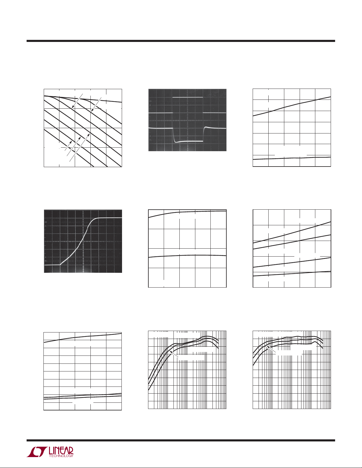
TYPICAL PERFORMANCE CHARACTERISTICS
Ideal Diode Resistance
Ideal Diode V-I Characteristics
1.0
0.8
0.6
0.4
CURRENT (A)
0.2
INTERNAL IDEAL DIODE
WITH SUPPLEMENTAL
EXTERNAL VISHAY
Si2333 PMOS
0
0.04
0
INTERNAL IDEAL
DIODE ONLY
0.12
0.08
FORWARD VOLTAGE (V)
V
0.16
BUS
USB Limited Load Current vs Battery
Voltage (Battery Charger Disabled)
900
800
700
600
500
400
300
LOAD CURRENT (mA)
200
100
0
2.7
3.0 3.6
BATTERY VOLTAGE (V)
3.3
V
BUS
5x MODE
3.9
= 5V
0.20
3576 G01
= 5V
4.2
3576 G04
vs Battery Voltage
0.25
0.20
INTERNAL IDEAL
0.15
0.10
RESISTANCE ()
0.05
0
3.0
2.7
Battery and V
vs Load Current
750
500
250
0
CURRENT (mA)
V
= 5V
BUS
BAT = 3.8V
–250
5x MODE
R
CLPROG
= 1k
R
PROG
–500
100 200 300
0
DIODE
INTERNAL IDEAL DIODE
WITH SUPPLEMENTAL
EXTERNAL VISHAY
Si2333 PMOS
3.6
3.3
BATTERY VOLTAGE (V)
Currents
BUS
V
CURRENT
BUS
BATTERY CURRENT
(CHARGING)
= 3.01k
BATTERY CURRENT
(DISCHARGING)
600 700 900
400 500
LOAD CURRENT (mA)
TA = 25°C unless otherwise specifi ed.
Voltage vs Load Current
V
OUT
(Battery Charger Disabled)
4.50
BAT = 4V
4.25
4.00
(V)
3.9
3576 G02
4.2
OUT
V
3.75
3.50
3.25
0
BAT = 3.4V
0.1 0.2 0.3
0.4 0.5
LOAD CURRENT (A)
Battery Charge Current vs
Temperature
600
R
= 2k
PROG
500
400
THERMAL REGULATION
040
TEMPERATURE (°C)
800
3576 G05
1000
300
200
CHARGE CURRENT (mA)
100
0
–40
–20 20
0.6 0.7 0.9
0.8
80
60
100
1.0
3576 G03
120
3576 G06
V
OUT
50mV/DIV
AC COUPLED
I
VOUT
500mA/DIV
0mA
PowerPath Switching Regulator
Transient Response
V
= 5V
BUS
= 3.65V
V
OUT
CHARGER OFF
10x MODE
20µs/DIV
3576 G07
PowerPath Switching Regulator
Effi ciency vs Load Current
100
90
1x MODE
80
70
60
EFFICIENCY (%)
50
40
30
10
5x, 10x MODE
100
LOAD CURRENT (mA)
3576 G08
1000
Battery Charging Effi ciency vs
Battery Voltage with No External
Load (P
95
R
CLPROG
R
90
PROG
85
80
75
70
EFFICIENCY (%)
65
5x MODE
60
55
50
2.7
BAT/PVBUS
= 3.01k
= 1k
3.0 3.6
BATTERY VOLTAGE (V)
)
1x MODE
3.3
3.9
4.2
3576 G09
3576f
7
Page 8
LTC3576/LTC3576-1
TYPICAL PERFORMANCE CHARACTERISTICS
V
Quiescent Current vs
BUS
V
Voltage (Suspend)
BUS
60
50
40
30
20
QUIESCENT CURRENT (µA)
10
0
0
1234
BUS VOLTAGE (V)
Battery Charge Current vs V
Voltage
600
R
= 3.01k
CLPROG
= 2k
R
PROG
500
5x MODE
400
300
200
BATTERY CURRENT (mA)
100
0
3.40
3.50 3.60
3.45 3.55
V
(V)
OUT
3.65
3.70
OUT
3.75
3576 G10
3576 G13
3.80
(V)
OUT
V
3.0
5
4.7
4.5
4.3
4.1
3.9
(V)
3.7
OUT
V
3.5
3.3
3.1
2.9
2.7
Voltage vs Load Current in
V
OUT
Suspend
5.0
4.5
3.5
2.5
4.0
0
V
HIGH POWER SUSPEND
LOW POWER SUSPEND
V
= 5V
BUS
BAT = 3.3V
= 3.01k
R
CLPROG
0.5
LOAD CURRENT (mA)
Voltage vs Battery Voltage
OUT
1.0
1.5
(Charger Overprogrammed)
V
= 5V
BUS
= 0V
I
VOUT
= 3.01k
R
CLPROG
= 1k
R
PROG
5x MODE
1x MODE
2.7
3.0
BATTERY VOLTAGE (V)
3.3
3.6
TA = 25°C unless otherwise specifi ed.
V
Current vs Load Current in
BUS
Suspend
2.5
V
= 5V
BUS
BAT = 3.3V
= 3.01k
R
CLPROG
2.0
1.5
HIGH POWER
SUSPEND
LOW POWER SUSPEND
0.5
0
1.0
LOAD CURRENT (mA)
2.0
3576 G11
2.5
CURRENT (mA)
1.0
BUS
V
0.5
0
Normalized Battery Charger Float
Voltage vs Temperature
1.001
1.000
0.999
0.998
0.997
NORMALIZED FLOAT VOLTAGE
3.9
3576 G14
4.2
0.996
–40
–15
10
TEMPERATURE (°C)
1.5
35
2.0
2.5
3576 G12
60
85
3576 G15
V
Quiescent Current vs
BUS
Temperature
25
V
= 5V
BUS
20
15
10
QUIESCENT CURRENT (mA)
5
0
–15
–40
8
5x MODE
1x MODE
35
10
TEMPERATURE (°C)
V
Quiescent Current in
BUS
Suspend vs Temperature
60
V
= 5V
BUS
50
40
30
20
QUIESCENT CURRENT (µA)
10
0
–40
60
85
3576 G16
–15 10 35 60
TEMPERATURE (°C)
85
3576 G17
Battery Drain Current vs
Temperature
35
30
25
20
15
10
BATTERY CURRENT (µA)
5
0
–15 10 35 85
–40
TEMPERATURE (°C)
BAT = 3.8V
= 0V
V
BUS
SWITCHING
REGULATORS OFF
60
3576 G18
3576f
Page 9
LTC3576/LTC3576-1
TYPICAL PERFORMANCE CHARACTERISTICS
OTG Boost Quiescent Current
vs V
Voltage
OUT
2.5
2.3
2.1
1.9
1.7
1.5
1.3
1.1
QUIESCENT CURRENT (mA)
0.9
0.7
0.5
2.90
3.55
4.20
V
(V)
OUT
OTG Boost Effi ciency
vs V
Voltage
OUT
95
500mA LOAD
90
85
80
EFFICIENCY (%)
75
100mA LOAD
4.85
3576 G19
5.50
OTG Boost V
vs Load Current
5.5
5.0
0 100
V
V
OUT
V
OUT
V
OUT
V
OUT
(V)
BUS
V
4.5
4.0
3.5
3.0
OTG Boost Start-Up Time into
Current Source Load vs V
Voltage
2.50
2.25
2.00
TIME (ms)
1.75
22µF ON V
22µF ON V
LOAD THROUGH OVP
Voltage
BUS
= 4.75V
BUS
I
= 500mA
VBUS
= 5V
= 4.4V
= 3.8V
= 3.2V
400
300
200
LOAD CURRENT (mA)
, 22µF AND
BUS
LOAD THROUGH OVP
22µF ON V
,
BUS
500
OUT
NO OVP
TA = 25°C unless otherwise specifi ed.
OTG Boost Effi ciency
vs Load Current
100
90
80
70
EFFICIENCY (%)
60
50
600
700
3576 G20
40
1
10 100 1000
LOAD CURRENT (mA)
OTG Boost Burst Mode Current
BUS
Threshold vs V
400
300
,
200
LOAD CURRENT (mA)
100
FALLING THRESHOLD
OUT
RISING THRESHOLD
Voltage
V
= 5V
OUT
= 4.4V
V
OUT
= 3.8V
V
OUT
= 3.2V
V
OUT
3576 G21
70
2.90
V
BUS
50mV/DIV
AC COUPLED
I
VBUS
200mA/DIV
0mA
3.55
1.50
2.9
4.20
V
OUT
(V)
4.85
5.50
3576 G22
3.4 3.9 4.4 4.9
V
(V)
OUT
5.4
3576 G23
0
2.90
3.55
V
4.20
OUT
(V)
4.85
5.50
3576 G24
OTG Boost Start-Up into Current
Source Load
50mV/DIV
I
VBUS
200mA/DIV
0mA
V
BUS
2V/DIV
0V
V
= 3.8V
OUT
20µs/DIV
3576 G25
V
I
LOAD
OUT
= 3.8V
= 500mA
200µs/DIV
AC COUPLED
3576 G26
V
BUS
V
1V/DIV
SW
OTG Boost Burst Mode OperationOTG Boost Transient Response
0V
OUT
I
LOAD
= 3.8V
= 10mA
50µs/DIVV
3576 G27
3576f
9
Page 10
LTC3576/LTC3576-1
TYPICAL PERFORMANCE CHARACTERISTICS
Battery Charging from USB-HV
USB OTG from BAT-HV BUCK-BAT
V
OUT
1V/DIV
V
BUS
I
BAT
0A
HVOK
5V/DIV
0V
V
V
BUS
5V/DIV
= 3.8V
BAT
= 285mA
I
BUS
= 12V
HV
IN
USING LT3653
500µs/DIV
V
OUT
1V/DIV
AC COUPLED
V
BUS
100mV/DIV
AC COUPLED
V
5V/DIV
HVOK
5V/DIV
V
BUS
5V/DIV
BUCK-USB
AC COUPLED
200mV/DIV
SW
0V
0V
V
BUS
HV
USING LT3653
IN
= 5V
= 12V
500µs/DIV
AC COUPLED
1A/DIV
3576 G28
OVP Connect Waveform OVP Disconnect Waveform
TA = 25°C unless otherwise specifi ed.
Oscillator Frequency vs
Temperature
2.30
2.25
2.20
2.15
FREQUENCY (MHz)
3576 G29
2.10
2.05
–40
–15
10
TEMPERATURE (°C)
Rising OVP Threshold vs
Temperature
6.280
6.275
V
= 5V
OUT
= 4.2V
V
OUT
= 3.6V
V
OUT
= 3V
V
OUT
= 2.7V
V
OUT
35
60
85
3576 G30
OVGATE
5V/DIV
OVP INPUT
VOLTAGE
0V TO 5V
STEP 5V/DIV
OVGATE vs OVSENS
12
OVSENS CONNECTED
TO INPUT THROUGH
6.2k RESISTOR
10
8
6
OVGATE (V)
4
2
0
0
OVP INPUT
STEP 5V/DIV
500µs/DIV
24 68
INPUT VOLTAGE (V)
3576 G31
3576 G34
OVGATE
5V/DIV
VOLTAGE
5V TO 10V
500µs/DIV
OVGATE Quiescent Current vs
Temperature
37
V
= 5V
OVSENS
35
33
31
QUIESCENT CURRENT (µA)
29
27
–40
–15
10
TEMPERATURE (°C)
6.270
6.265
OVP THRESHOLD (V)
3576 G32
6.260
6.255
–40
–15
10
TEMPERATURE (°C)
35
60
85
3576 G33
RST3, CHRG Pin Current vs
Voltage (Pull-Down State)
100
V
= 5V
BUS
BAT = 3.8V
80
60
40
20
RST3, CHRG PIN CURRENT (mA)
35
60
85
3576 G35
0
1
0
RST3, CHRG PIN VOLTAGE (V)
3
4
2
5
3576 G36
10
3576f
Page 11
LTC3576/LTC3576-1
TYPICAL PERFORMANCE CHARACTERISTICS
3.3V LDO Output Voltage vs
Load Current, V
3.4
BAT = 3.9V, 4.2V
3.2
3.0
OUTPUT VOLTAGE (V)
BAT = 3V
2.8
BAT = 3.1V
BAT = 3.2V
BAT = 3.3V
2.6
5
0
LOAD CURRENT (mA)
10
= 0V
BUS
BAT = 3.4V
15
Switching Regulator Soft-Start
Waveform
500mV/DIV
OUT
V
50µs/DIV
BAT = 3.5V
BAT = 3.6V
20
3576 G37
3576 G40
20mV/DIV
AC COUPLED
25
3.3V LDO Step Response
(5mA to 15mA)
I
LDO3V3
5mA/DIV
0mA
V
LDO3V3
20µs/DIVBAT = 3.8V
Switching Regulator Current Limit
vs Temperature
2.0
REGULATOR 3
1.5
1.0
CURRENT LIMIT (A)
0.5
V
IN1,2,3
0
–40
REGULATORS 1, 2
= 3.8V
–15
10
TEMPERATURE (°C)
35
TA = 25°C unless otherwise specifi ed.
Battery Drain Current vs
Battery Voltage
35
I
= 0mA
VOUT
30
V
= 0V
BUS
25
20
15
10
3576 G38
BATTERY CURRENT (µA)
5
0
2.7
R
DS(ON)
V
BUS
(SUSPEND MODE)
3.0 3.3 3.6 4.2
BATTERY VOLTAGE (V)
for Switching Regulator
Power Switches vs Temperature
1.0
0.8
NMOS SWITCH
0.6
PMOS SWITCH
0.4
ON-RESISTANCE (Ω)
NMOS SWITCH
0.2
PMOS SWITCH
0
–15
60
85
3576 G41
–40
10
TEMPERATURE (°C)
= 5V
3.9
REGULATORS 1, 2
REGULATOR 3
35
60
3576 G39
85
3576 G42
Switching Regulator Low Power
Quiescent Currents vs Temperature
100
90
80
70
60
50
40
30
QUIESCENT CURRENTS (μA)
20
10
0
–40
PULSE-SKIP MODE
Burst Mode OPERATION
LDO MODE
–15
10
TEMPERATURE (°C)
35
Switching Regulators 1, 2
Pulse-Skip Mode Effi ciency
100
V
= 3.8V
IN3
90
80
70
60
50
40
EFFICIENCY (%)
30
20
10
0
60
85
3576 G43
0.1 10 100 1000
V
= 2.5V
OUT1,2
V
OUT1,2
V
= 1.8V
OUT1,2
1
LOAD CURRENT (mA)
= 1.2V
3576 G44
Switching Regulators 1, 2
Burst Mode Effi ciency
100
V
IN3
90
80
70
60
50
40
EFFICIENCY (%)
30
20
10
0
0.1 10 100 1000
V
= 3.8V
OUT1,2
V
OUT1,2
1
LOAD CURRENT (mA)
= 2.5V
V
OUT1,2
= 1.8V
= 1.2V
3576 G45
3576f
11
Page 12
LTC3576/LTC3576-1
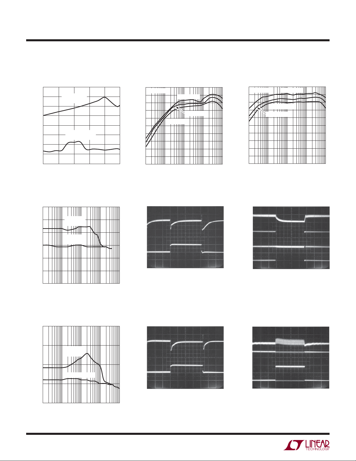
TYPICAL PERFORMANCE CHARACTERISTICS
Switching Regulator Constant
Frequency Quiescent Currents
8
7
6
5
4
3
2
QUIESCENT CURRENT (mA)
1
0
–40
SWITCHING
REGULATOR 3
SWITCHING
REGULATORS 1, 2
–15 10 60
TEMPERATURE (°C)
35
Switching Regulators 1, 2
Feedback Voltage vs Load Current
0.820
0.815
0.810
0.805
0.800
FEEDBACK VOLTAGE (V)
0.795
0.790
0.1 10 100 1000
Burst Mode
OPERATION
PULSE-SKIP
MODE
1
LOAD CURRENT (mA)
Switching Regulator 3 Feedback
Voltage vs Load Current
0.810
85
3576 G46
50mV/DIV
AC COUPLED
200mA/DIV
3576 G49
Switching Regulator 3
Pulse-Skip Mode Effi ciency
100
V
= 3.8V
IN3
90
80
70
60
50
40
EFFICIENCY (%)
30
20
10
0
0.1 10 100 1000
V
= 2.5V
OUT3
V
OUT3
V
= 1.2V
OUT3
1
LOAD CURRENT (mA)
= 1.8V
Switching Regulators 1, 2
Transient Response
V
OUT2
I
OUT2
0mA
V
V
IN2
OUT2
= 3.8V
= 3.4V
50µs/DIV
Switching Regulator 3
Transient Response
TA = 25°C unless otherwise specifi ed.
Switching Regulator 3
Burst Mode Effi ciency
100
V
3576 G47
= 3.8V
IN3
90
80
70
60
50
40
EFFICIENCY (%)
30
20
10
0
0.1 10 100 1000
V
OUT3
V
= 1.2V
OUT3
V
= 1.8V
OUT3
1
LOAD CURRENT (mA)
Switching Regulator Mode
Transition, Pulse Skip-LDOPulse Skip
V
OUT3
50mV/DIV
AC COUPLED
V
SW3
1V/DIV
0V
3576 G50
V
V
I
OUT3
IN3
OUT3
= 3.8V
= 1.8V
= 50mA
50µs/DIV
Switching Regulator Mode
Transition, Pulse Skip–Burst
Mode Operation–Pulse Skip
= 2.5V
3576 G48
3576 G51
0.805
0.800
FEEDBACK VOLTAGE (V)
0.795
0.790
0.1 10 100 1000
Burst Mode
OPERATION
PULSE SKIP MODE
1
LOAD CURRENT (mA)
12
3576 G52
V
OUT3
50mV/DIV
AC COUPLED
I
OUT3
500mA/DIV
0mA
V
V
IN3
OUT3
= 3.8V
= 1.8V
50µs/DIV
3576 G53
V
OUT3
50mV/DIV
AC COUPLED
V
SW3
1V/DIV
0V
V
IN3
V
OUT3
I
OUT3
= 3.8V
= 1.8V
= 100mA
50µs/DIV
3576 G54
3576f
Page 13

PIN FUNCTIONS
LTC3576/LTC3576-1
CLPROG (Pin 1): USB Current Limit Program and Monitor
Pin. A 1% resistor from CLPROG to ground determines
the upper limit of the current drawn or sourced from the
pins. A precise fraction, h
V
BUS
CLPROG
, of the V
BUS
current is sent to the CLPROG pin when the PMOS switch of
the PowerPath switching regulator is on. The switching
regulator delivers power until the CLPROG pin reaches
1.18V in step-down mode and 1.15V in step-up mode.
When the switching regulator is in step-down mode,
CLPROG is used to regulate the average input current.
Several V
current limit settings are available via user
BUS
input which will typically correspond to the 500mA and
100mA USB specifi cations. When the switching regulator
is in step-up mode (USB on-the-go), CLPROG is used to
limit the average output current to 680mA. A multilayer
ceramic averaging capacitor or R-C network is required
at CLPROG for fi ltering.
LDO3V3 (Pin 2): 3.3V LDO Output Pin. This pin provides
a regulated always-on 3.3V supply voltage. LDO3V3
gets its power from V
. It may be used for light loads
OUT
such as a watchdog microprocessor or real time clock.
A 1µF capacitor is required from LDO3V3 to ground. If
the LDO3V3 output is not used it should be disabled by
connecting it to V
OUT
.
NTCBIAS (Pin 3): NTC Thermistor Bias Output. If NTC
operation is desired, connect a bias resistor between
NTCBIAS and NTC, and an NTC thermistor between NTC
and GND. To disable NTC operation, connect NTC to GND
and leave NTCBIAS open.
NTC (Pin 4): Input to the Thermistor Monitoring Circuits.
The NTC pin connects to a negative temperature coeffi cient
thermistor, which is typically co-packaged with the battery,
to determine if the battery is too hot or too cold to charge.
If the battery’s temperature is out of range, charging is
paused until it re-enters the valid range. A low drift bias
resistor is required from NTCBIAS to NTC and a thermistor
is required from NTC to ground. To disable NTC operation,
connect NTC to GND and leave NTCBIAS open.
OVGATE (Pin 5): Overvoltage Protection Gate Output.
Connect OVGATE to the gate pin of an external N-channel
MOS pass transistor. The source of the transistor should
be connected to V
and the drain should be connected
BUS
to the product’s DC input connector. In the absence of an
overvoltage condition, this pin is connected to an internal
charge pump capable of creating suffi cient overdrive to fully
enhance the pass transistor. If an overvoltage condition is
detected, OVGATE is brought rapidly to GND to prevent
damage to the LTC3576/LTC3576-1. OVGATE works in
conjunction with OVSENS to provide this protection.
OVSENS (Pin 6): Overvoltage Protection Sense Input.
OVSENS should be connected through a 6.2k resistor to
the input power connector and the drain of an external
N-channel MOS pass transistor. When the voltage on this
pin exceeds
V
OVCUTOFF
,
the OVGATE pin will be pulled
to GND to disable the pass transistor and protect the
LTC3576/LTC3576-1. The OVSENS pin shunts current
during an overvoltage transient in order to keep the pin
voltage at 6V.
FB1 (Pin 7): Feedback Input for Switching Regulator 1.
When regulator 1’s control loop is complete, this pin servos
to 1 of 16 possible set points based on the commanded
2
value from the I
(Pin 8): Power Input for Switching Regulator 1.
V
IN1
This pin will generally be connected to V
C serial port. See Table 4.
OUT
. A 1µF MLCC
capacitor is recommended on this pin.
SW1 (Pin 9): Power Transmission Pin for Switching
Regulator 1.
EN1 (Pin 10): Logic Input. This logic input pin indepen-
dently enables switching regulator 1. Active high. This
pin is logically ORed with its corresponding bit in the
2
C serial port. See Table 3. Has a 2µA internal pull-down
I
current source.
ENOTG (Pin 11): Logic Input. This logic input pin independently enables the bidirectional switching regulator to
step up the voltage on V
for USB on-the-go applications. Active high. This
V
BUS
and provide a 5V output on
OUT
pin is logically ORed with its corresponding bit in the
2
C serial port. See Table 3. Has a 2µA internal pull-down
I
current source.
3576f
13
Page 14

LTC3576/LTC3576-1
PIN FUNCTIONS
DVCC (Pin 12): Logic Supply for the I2C Serial Port. If the
serial port is not needed, it can be disabled by grounding
. When DVCC is grounded, the I2C bits are set to their
DV
CC
default values. See Table 3.
2
SCL (Pin 13): Clock Input Pin for the I
2
C logic levels are scaled with respect to DVCC. If DVCC
I
C Serial Port. The
is grounded, the SCL pin is equivalent to the C2, C4 and
2
C6 bits in the I
C serial port. SCL in conjunction with SDA
determine the operating modes of switching regulators 1,
2 and 3 when DV
is grounded. See Tables 3 and 5. Has
CC
a 2µA internal pull-down current source.
2
SDA (Pin 14): Data Input Pin for the I
2
C logic levels are scaled with respect to DVCC. If DVCC
I
C Serial Port. The
is grounded, the SDA pin is equivalent to the C3, C5 and
2
C7 bits in the I
C serial port. SDA in conjunction with SCL
determine the operating modes of switching regulators 1,
2 and 3 when DV
is grounded. See Tables 3 and 5. Has
CC
a 2µA internal pull-down current source.
NC (Pin 15): Unconnected Pin. This pin is not connected
internally to the part. It is permissible to tie this pin to V
in order to make the V
(Pin 16): Power Input for Switching Regulator 3.
V
IN3
This pin will generally be connected to V
PCB trace wider.
IN3
. A 1µF MLCC
OUT
IN3
capacitor is recommended on this pin.
SW3 (Pin 17): Power Transmission Pin for Switching
Regulator 3.
NC (Pin 18): Unconnected Pin. This pin is not connected
internally to the part. It is permissible to tie this pin to SW3
in order to make the SW3 PCB trace wider.
EN3 (Pin 19): Logic Input. This logic input pin independently enables switching regulator 3. Active high. This
pin is logically ORed with its corresponding bit in the
2
C serial port. See Table 3. Has a 2µA internal pull-down
I
current source.
FB3 (Pin 20): Feedback Input for Switching Regulator 3.
When regulator 3’s control loop is complete, this pin servos
to 1 of 16 possible set points based on the commanded
2
value from the I
C serial port. See Table 4.
RST3 (Pin 21): Logic Output. This in an open-drain output
which indicates that switching regulator 3 has settled to
its fi nal value. It can be used as a power-on reset for the
primary microprocessor or to enable the other switching
regulators for supply sequencing.
EN2 (Pin 22): Logic Input. This logic input pin independently enables switching regulator 2. Active high. This
pin is logically ORed with its corresponding bit in the
2
C serial port. See Table 3. Has a 2µA internal pull-down
I
current source.
SW2 (Pin 23): Power Transmission Pin for Switching
Regulator 2.
(Pin 24): Power Input for Switching Regulator 2.
V
IN2
This pin will generally be connected to V
. A 1µF MLCC
OUT
capacitor is recommended on this pin.
FB2 (Pin 25): Feedback Input for Switching Regulator 2.
When regulator 2’s control loop is complete, this pin servos
to 1 of 16 possible set points based on the commanded
2
value from the I
(Pin 26): Bat-Track External Switching Regulator Control
V
C
Output. This pin drives the V
C serial port. See Table 4.
pin of an external Linear
C
Technology step-down switching regulator. An external Pchannel MOSFET is sometimes required to provide power
to V
with its gate tied to the ACPR pin (see Applications
OUT
Information). In concert with WALL and ACPR, it will
regulate V
to maximize battery charger effi ciency
OUT
WALL (Pin 27): External Power Source Sense Input. WALL
should be connected to the output of the external high
voltage switching regulator and to the drain of an external
P-channel MOSFET if used. It is used to determine when
power is applied to the external regulator. When power
is detected, ACPR is driven low and the USB input is automatically disabled. Pulling this pin above 4.3V enables
pin.
the V
C
14
3576f
Page 15

PIN FUNCTIONS
LTC3576/LTC3576-1
ACPR (Pin 28): External Power Source Present Output
(Active Low). ACPR indicates that the output of the external
high voltage step-down switching regulator is suitable for
use by the LTC3576/LTC3576-1. It should be connected to
the gate of an external P-channel MOSFET whose source
is connected to V
WALL. ACPR has a high level of V
and whose drain is connected to
OUT
and a low level of
OUT
GND. The USB bidirectional switcher is disabled when
ACPR is low.
PROG (Pin 29): Charge Current Program and Charge Current Monitor Pin. Connecting a 1% resistor from PROG
to ground programs the charge current. If suffi cient input
power is available in constant-current mode, this pin servos
to 1V. The voltage on this pin always represents the actual
charge current by using the following formula:
V
I
BAT
PROG
= • 1030
R
PROG
CHRG (Pin 30): Open-Drain Charge Status Output. The
CHRG pin indicates the status of the battery charger.
Four possible charger states are represented by CHRG:
charging, not charging, unresponsive battery and battery
temperature out of range. In addition, CHRG is used to
indicate whether there is a short-circuit condition on V
BUS
when the bidirectional switching regulator is in step-up
mode (on-the-go). CHRG is modulated at 35kHz and
switches between a low and a high duty cycle for easy
recognition by either humans or microprocessors. See
Table 1. CHRG requires a pull-up resistor and/or LED to
provide indication.
IDGATE (Pin 31): Ideal Diode Amplifi er Output. This pin
controls the gate of an optional external P-channel MOSFET
used as an ideal diode between V
and BAT. The external
OUT
ideal diode operates in parallel with the internal ideal diode.
The source of the P-channel MOSFET should be connected
to V
and the drain should be connected to BAT. If the
OUT
external ideal diode MOSFET is not used, IDGATE should
be left fl oating.
BAT (Pin 32): Single Cell Li-Ion Battery Pin. Depending on
available V
deliver power to V
from V
V
OUT
(Pin 33): Output Voltage of the Bidirectional Pow-
OUT
power, a Li-Ion battery on BAT will either
BUS
through the ideal diode or be charged
OUT
via the battery charger.
erPath Switching Regulator in step-down mode and
Input Voltage of the Battery Charger. The majority of
the portable product should be powered from V
OUT
. The
LTC3576/LTC3576-1 will partition the available power
between the external load on V
and the internal bat-
OUT
tery charger. Priority is given to the external load and any
extra power is used to charge the battery. An ideal diode
from BAT to V
ensures that V
OUT
the load exceeds the allotted power from V
power source is removed. In on-the-go mode, this
V
BUS
pin delivers power to V
via the SW pin. V
BUS
is powered even if
OUT
or if the
BUS
should
OUT
be bypassed with a low impedance ceramic capacitor.
V
(Pins 34, 35): Power Pins. These pins deliver power
BUS
to V
via the SW pin by drawing controlled current from
OUT
a DC source such as a USB port or DC output wall adapter.
In on-the-go mode these pins provide power to external
loads. Tie the two V
pins together at the part and bypass
BUS
with a low impedance multilayer ceramic capacitor.
SW (Pin 36): The SW pin transfers power between V
and V
via the bidirectional switching regulator. See
OUT
BUS
the Applications Information section for a discussion of
inductance value and current rating.
, I
I
LIM0
(Pins 37, 38): I
LIM1
LIM0
and I
control the current
LIM1
limit of the PowerPath switching regulator. See Table 1.
Both the I
LIM0
and I
corresponding bits in the I
pins are logically ORed with their
LIM1
2
C serial port. See Tables 3 and
6. Each has a 2µA internal pull-down current source.
Exposed Pad (Pin 39): Ground. The Exposed Pad should
be connected to a continuous ground plane on the second
layer of the printed circuit board by several vias directly
under the LTC3576/LTC3576-1.
3576f
15
Page 16

LTC3576/LTC3576-1
BLOCK DIAGRAM
OVSENS
OVGATE
V
BUS
V
BUS
6
5
35
34
OVP
SUSPEND LDO
500µA/2.5mA
2.25MHz
BIDIRECTIONAL
PowerPath
SWITCHING
REGULATOR
V
C
26
V
C
CONTROL
WALL
DETECT
3.3V LDO
27
28
36
2
33
WALL
ACPR
SW
LDO3V3
V
OUT
CLPROG
NTCBIAS
NTC
CHRG
I
LIM0
I
LIM1
ENOTG
EN1
EN2
EN3
DV
SDA
SCL
–
+
+
3.6V
D/A
D/A
4
D/A
4
CC/CV
CHARGER
0.3V
–
+
IDEAL
ENABLE
400mA 2.25MHz
BUCK
REGULATOR
ENABLE
400mA 2.25MHz
BUCK
REGULATOR
ENABLE
1A 2.25MHz
BUCK
REGULATOR
5.1V
1.18V
–
+
–
+
4
1
3
4
30
37
38
11
10
22
19
12
CC
14
13
BATTERY
TEMPERATURE
MONITOR
CHARGE
STATUS
I
LIM
DECODE
LOGIC
OR 1.15V
I2C PORT
+
–
–
+
15mV
31
32
29
24
23
25
16
17
20
21
8
9
7
IDGATE
BAT
PROG
V
IN1
SW1
FB1
V
IN2
SW2
FB2
V
IN3
SW3
FB3
RST3
16
39
GND
3576 BD
3576f
Page 17

TIMING DIAGRAM
SDA
t
SU,DAT
t
HIGH
t
r
SCL
t
HD,STA
START
CONDITION
t
LOW
I2C WRITE PROTOCOL
LTC3576/LTC3576-1
t
SU,STA
t
HD,DAT
t
f
REPEATED START
CONDITION
t
HD,STA
t
SP
CONDITION
STOP
t
SU,STO
t
BUF
3208 F05
START
CONDITION
SDA
SCL
WRITE ADDRESS R/W
00010010
00 010 01 0
123
456789123456789123456789
SUB-ADDRESS
A7 A6 A5 A4 A3 A2 A1 A0
ACK
INPUT DATA BYTE
B7 B6 B5 B4 B3 B2 B1 B0
ACK
STOPSTART
ACK
3576 I2C
3576f
17
Page 18

LTC3576/LTC3576-1
OPERATION
Introduction
The LTC3576/LTC3576-1 are highly integrated power management ICs designed to make optimal use of the power
available from a variety of sources, while minimizing power
dissipation and easing thermal budgeting constraints.
They include a high effi ciency bidirectional PowerPath
switching regulator, a controller for an external high voltage step-down switching regulator, a battery charger, an
ideal diode, an always-on LDO, an overvoltage protection
circuit and three general purpose step-down switching
regulators. The entire chip is controlled by either direct
2
digital control or by an I
C serial port or both.
The innovative PowerPath architecture ensures that the
application is powered immediately after external voltage is
applied, even with a completely dead battery, by prioritizing
power to the application.
When acting as a step-down converter, the LTC3576/
LTC3576-1’s bidirectional switching regulator takes
power from USB, wall adapters, or other 5V sources and
provides power to the application and effi ciently charges
the battery using Bat-Track. Because power is conserved
the LTC3576/LTC3576-1 allow the load current on V
OUT
to
exceed the current drawn by the USB port making maximum use of the allowable USB power for battery charging.
For USB compatibility the switching regulator includes
a precision average input current limit. The PowerPath
switching regulator and battery charger communicate to
ensure that the average input current never exceeds the
USB specifi cations.
Additionally, the bidirectional switching regulator can also
operate as a 5V synchronous step-up converter taking
power from V
and delivering up to 500mA to V
OUT
BUS
without the need for any additional external components.
This enables systems with USB dual-role transceivers to
function as USB on-the-go dual-role devices. True output
disconnect and average output current limit features are
included for short-circuit protection.
For automotive, fi rewire, and other high voltage applications, the LTC3576/LTC3576-1 provide Bat-Track control of
an external LTC step-down switching regulator to maximize
battery charger effi ciency and minimize heat production.
When power is available from both the USB and an auxiliary
input, the auxiliary input is given priority.
The LTC3576/LTC3576-1 contain both an internal 180mΩ
ideal diode as well as an ideal diode controller for use
with an optional external P-channel MOSFET. The ideal
diode(s) from BAT to V
is always available to V
absent power at V
BUS
guarantee that ample power
OUT
even if there is insuffi cient or
OUT
or WALL.
An “always-on” LDO provides a regulated 3.3V from
available power at V
. Drawing very little quiescent
OUT
current, this LDO will be on at all times and can be used
to supply 20mA.
The LTC3576/LTC3576-1 feature an overvoltage protection
circuit which is designed to work with an external N-channel MOSFET to prevent damage to their inputs caused by
accidental application of high voltage.
To prevent battery drain when a device is connected to a
suspended USB port, an LDO from V
BUS
to V
provides
OUT
either low power or high power USB suspend current to
the application.
The three general purpose switching regulators can be
independently enabled either by direct digital control or
2
by operating the I
C serial port. Under I2C control, all
three switching regulators have adjustable set points so
that voltages can be reduced when high processor performance is not needed. Along with constant frequency PWM
mode, all three switching regulators have automatic Burst
Mode operation and LDO modes for signifi cantly reduced
quiescent current under light load conditions.
18
3576f
Page 19

OPERATION
LTC3576/LTC3576-1
Bidirectional PowerPath Switching Regulator—
Step-Down Mode
The power delivered from V
BUS
to V
is controlled by
OUT
a 2.25MHz constant frequency bidirectional switching
regulator operating in step-down mode. V
drives the
OUT
combination of the external load (step-down switching
regulators 1, 2 and 3) and the battery charger. To meet the
maximum USB load specifi cation, the switching regulator
contains a measurement and control system that ensures
that the average input current remains below the level
programmed at CLPROG.
If the combined load does not cause the switching regulator to reach the programmed input current limit, V
OUT
will track approximately 0.3V above the battery voltage.
By keeping the voltage across the battery charger at this
low level, power lost to the battery charger is minimized.
Figure 1 shows the power fl ow in step-down mode.
If the combined external load plus battery charge current
is large enough to cause the switching regulator to reach
the programmed input current limit, the battery charger
will reduce its charge current by precisely the amount
necessary to enable the external load to be satisfi ed. Even
if the battery charge current is programmed to exceed the
allowable USB current, the USB specifi cation for average
input current will not be violated; the battery charger will
reduce its current as needed. Furthermore, if the load current at V
exceeds the programmed power from V
OUT
BUS
,
load current will be drawn from the battery via the ideal
diode(s) even when the battery charger is enabled.
The current out of CLPROG is a precise fraction of the V
BUS
current. When a programming resistor and an averaging
capacitor are connected from CLPROG to GND, the voltage on CLPROG represents the average input current of
the switching regulator. As the input current approaches
the programmed limit, CLPROG reaches 1.18V and power
delivered by the switching regulator is held constant.
TO USB
OR WALL
ADAPTER
TO AUTOMOTIVE,
FIREWIRE, ETC.
HIGH VOLTAGE
6
5
35
34
1
OVSENS
OVGATE
V
BUS
V
BUS
I
SWITCH
CLPROG
OVERVOLTAGE PROTECTION
/N
s2
V
BUS
VOLTAGE
CONTROLLER
–
+
5V
–
+
+
PWM AND
GATE DRIVE
6V
–
–
+
1.18V 3.6V
AVERAGE V
CURRENT LIMIT
CONTROLLER
BUS
INPUT
V
OUT
CONTROLLER
26
V
VOLTAGE
V
IN
STEP-DOWN
SWITCHING
V
C
REGULATOR
C
–
0.3V
+
+
+
SW
FB
CONSTANT CURRENT
CONSTANT VOLTAGE
BATTERY CHARGER
–
27
V
OUT
3.6V
BAT + 0.3V
IDEAL
DIODE
OmV
15mV
WALL
4.3V
–
+
–
+
+
Bat-Track HV CONTROL
+
–
Figure 1. PowerPath Block Diagram—Power Available from USB/Wall Adapter
–
+
IDGATE
USB INPUT
BATTERY POWER
HV INPUT
ACPR
SW
V
OUT
BAT
28
3.5V TO
36
33
31
32
+
3576 F01
(BAT + 0.3V)
TO SYSTEM LOAD
OPTIONAL EXTERNAL
IDEAL DIODE PMOS
SINGLE CELL
Li-Ion
3576f
19
Page 20

LTC3576/LTC3576-1
OPERATION
The input current limit is programmed by the I
pins or by the I2C serial port. The input current limit
I
LIM1
LIM0
and
has fi ve possible settings ranging from the USB suspend
limit of 500µA up to 1A for wall adapter applications. Two
of these settings are specifi cally intended for use in the
100mA and 500mA USB applications. Refer to Table 1 for
current limit settings using the I
LIM0
and I
Table 6 for current limit settings using the I
Table 1. USB Current Limit Settings Using I
I
LIM1
00
01
1 0 Low Power Suspend (USB 500µA Limit)
11
I
LIM0
USB SETTING
1× Mode (USB 100mA Limit)
10× Mode (Wall 1A Limit)
5× Mode (USB 500mA Limit)
LIM0
LIM1
2
and I
pins and
C port.
LIM1
When the switching regulator is activated, the average
input current will be limited by the CLPROG programming
resistor according to the following expression:
V
II
=+ +
VBUS VBUSQ
where I
LTC3576-1, V
is the quiescent current of the LTC3576/
VBUSQ
CLPROG
current limit, R
resistor and h
rent at V
to the sample current delivered to CLPROG.
BUS
CLPROG
CLPROG
CLPROG
R
CLPROG
h
•1
()
CLPROG
is the CLPROG servo voltage in
is the value of the programming
is the ratio of the measured cur-
Refer to the Electrical Characteristics table for values of
h
CLPROG
, V
CLPROG
and I
. Given worst-case circuit
VBUSQ
tolerances, the USB specifi cation for the average input
current in 100mA or 500mA mode will not be violated,
provided that R
CLPROG
is 3.01k or greater.
While not in current limit, the switching regulator’s BatTrack feature will set V
to approximately 300mV above
OUT
the voltage at BAT. However, if the voltage at BAT is below
3.3V, and the load requirement does not cause the switching regulator to exceed its current limit, V
will regulate
OUT
at a fi xed 3.6V as shown in Figure 2. This “instant-on”
operation will allow a portable product to run immediately
when power is applied without waiting for the battery to
charge. If the load does exceed the current limit at V
will range between the no-load voltage and slightly
V
OUT
BUS
,
below the battery voltage, indicated by the shaded region
of Figure 2.
4.5
4.2
3.9
2.4
NO LOAD
2.7 3.0
Figure 2. V
300mV
3.6 4.2
3.3 3.9
BAT (V)
vs BAT
OUT
3576 F02
(V)
OUT
V
3.6
3.3
3.0
2.7
2.4
For very low-battery voltages, the battery charger acts like a
load and, due to limited input power, its current will tend to
pull V
V
OUT
automatically detects that V
below the 3.6V “Instant On” voltage. To prevent
OUT
from falling below this level, an undervoltage circuit
is falling and reduces the
OUT
battery charge current as needed. This reduction ensures
that load current and voltage are always prioritized while
allowing as much battery charge current as possible. See
Over Programming the Battery Charger in the Applications
Information section.
The voltage regulation loop is compensated by the capacitance on V
. A 10µF MLCC capacitor is required
OUT
for loop stability. Additional capacitance beyond this value
will improve transient response.
An internal undervoltage lockout circuit monitors V
keeps the switching regulator off until V
rises above
BUS
BUS
and
4.30V and is about 200mV above the battery voltage.
Hysteresis on the UVLO turns off the regulator if V
BUS
falls below 4V or to within 50mV of the battery voltage.
When this happens, system power at V
will be drawn
OUT
from the battery via the ideal diode(s).
Bidirectional PowerPath Switching Regulator—
Step-Up Mode
For USB on-the-go applications, the bidirectional
PowerPath switching regulator acts as a step-up converter
to deliver power from V
OUT
to V
. The power from V
BUS
OUT
can come from the battery or the output of the external
20
3576f
Page 21

OPERATION
LTC3576/LTC3576-1
TO USB
CABLE
TO AUTOMOTIVE,
FIREWIRE, ETC.
6
5
35
34
1
OVSENS
OVGATE
V
BUS
V
BUS
I
SWITCH
CLPROG
OVERVOLTAGE PROTECTION
V
VOLTAGE
OUTPUT
BUS
BUS
–
+
+
GATE DRIVE
–
+
s2
CONTROLLER
/N
5V
–
+
1.15V 3.6V
AVERAGE V
CURRENT LIMIT
CONTROLLER
6V
–
PWM AND
Figure 3. PowerPath Block Diagram—USB On-the-Go
26
V
C
–
+
+
V
VOLTAGE
OUT
CONTROLLER
HIGH VOLTAGE
V
IN
STEP-DOWN
SWITCHING
V
C
REGULATOR
CONSTANT CURRENT
0.3V
+
SW
FB
CONSTANT VOLTAGE
BATTERY CHARGER
–
27
V
OUT
3.6V
BAT + 0.3V
IDEAL
DIODE
OmV
15mV
–
+
4.3V
WALL
+
–
–
+
+
Bat-Track HV CONTROL
–
+
BATTERY POWER
HV INPUT
ACPR
V
OUT
IDGATE
BAT
28
SW
36
33
31
32
+
3576 F03
3.5V TO
(BAT + 0.3V)
TO SYSTEM LOAD
OPTIONAL EXTERNAL
IDEAL DIODE PMOS
SINGLE CELL
Li-Ion
high voltage switching regulator. As a step-up converter,
the bidirectional switching regulator produces 5V on
and is capable of delivering at least 500mA. USB
V
BUS
on-the-go can be enabled by either the external control
2
pin, ENOTG, or via I
C. Figure 3 shows the power fl ow
in step-up mode.
An undervoltage lockout circuit monitors V
vents step-up conversion until V
prevent backdriving of V
the V
conversion if V
undervoltage lockout circuit prevents step-up
BUS
is greater than 4.3V at the time step-up
BUS
when input power is available,
BUS
rises above 2.8V. To
OUT
and pre-
OUT
mode is enabled. The switching regulator is also designed
to allow true output disconnect by eliminating body diode
conduction of the internal PMOS switch. This allows V
BUS
to go to zero volts during a short-circuit condition or while
shut down, drawing zero current from V
OUT
.
The voltage regulation loop is compensated by the capacitance on V
. A 4.7µF MLCC is required for loop stability.
BUS
Additional capacitance beyond this value will improve
transient response. The V
voltage has approximately
BUS
3% load regulation up to an output current of 500mA. At
light loads, the switching regulator goes into Burst Mode
operation. The regulator will deliver power to V
BUS
until it
reaches 5.1V after which the NMOS and PMOS switches
shut off. The regulator delivers power again to V
BUS
once
it falls below 5.1V.
The switching regulator features both peak inductor and
average output current limit. The peak current mode
architecture limits peak inductor current on a cycle-bycycle basis. The peak current limit is equal to V
BUS
/2 to
a maximum of 1.8A so that in the event of a sudden short
circuit, the current limit will fold back to a lower value.
In step-up mode, the voltage on CLPROG represents the
average output current of the switching regulator when
a programming resistor and an averaging capacitor are
connected from CLPROG to GND. With a 3.01k resistor
on CLPROG, the bidirectional switching regulator has an
output current limit of 680mA. As the output current approaches this limit CLPROG servos to 1.15V and V
BUS
falls
3576f
21
Page 22

LTC3576/LTC3576-1
OPERATION
rapidly to V
. When V
OUT
is close to V
BUS
there may not
OUT
be suffi cient negative slope on the inductor current when
the PMOS switch is on to balance the rise in the inductor
current when the NMOS switch is on. This will cause the
inductor current to run away and the voltage on CLPROG
to rise. When CLPROG reaches 1.2V the switching of the
synchronous PMOS is terminated and V
is applied
OUT
statically to its gate. This ensures that the inductor current
will have suffi cient negative slope during the time current
is fl owing to the output. The PMOS will resume switching
when CLPROG drops down to 1.15V.
The LTC3576/LTC3576-1 maintain voltage regulation even
if V
PMOS switch. The PMOS switch is enabled when V
rises above V
below V
is above V
OUT
OUT
. This is achieved by disabling the
BUS
BUS
+ 180mV and is disabled when it falls
OUT
+ 70mV to prevent the inductor current from
running away when not in current limit. Since the PMOS
no longer acts as a low impedance switch in this mode,
there will be more power dissipation within the IC. This
will cause a sharp drop in effi ciency.
If V
is less than 4V and the PMOS switch is disabled
BUS
for more than 7.2ms a short-circuit fault will be declared
and the part will shut off. The CHRG pin will blink at 35kHz
with a duty cycle that varies between 12% and 88% at a
4Hz rate. See Table 2. To re-enable step-up mode, the
ENOTG pin or, with ENOTG grounded, the B0 bit in the
2
C port must be cycled low and then high.
I
Bat-Track Auxiliary High Voltage Switching Regulator
Control
The WALL, ACPR and
VC pins can be used in conjunction
with an external high voltage step-down switching regula-
®
tor such as the LT
3480 or the LT3653 to minimize heat
production when operating from higher voltage sources,
as shown in Figures 1 and 3. Bat-Track control circuitry
regulates the external switching regulator’s output voltage
to the larger of (BAT + 300mV) or 3.6V. This maximizes
battery charger effi ciency while still allowing instant-on
operation when the battery is deeply discharged.
The feedback network of the high voltage regulator
should be set to generate an output voltage between 4.5V
and 5.5V. When high voltage is applied to the external
regulator, WALL will rise toward this programmed output
voltage. When WALL exceeds approximately 4.3V, ACPR
is brought low and the Bat-Track control of the LTC3576/
LTC3576-1 overdrives the local V
control of the external
C
high voltage step-down switching regulator. Therefore,
once the Bat-Track control is enabled, the output voltage
is set independent of the switching regulator feedback
network.
Bat-Track control provides a signifi cant effi ciency advantage
over the simple use of a 5V switching regulator output to
drive the battery charger. With a 5V output driving V
OUT
,
battery charger effi ciency is approximately:
V
η
TOTAL
where
η
=η
BUCK
is the effi ciency of the high voltage switching
BUCK
BAT
•
5V
regulator and 5V is the output voltage of the switching
regulator. With a typical switching regulator effi ciency of
87% and a typical battery voltage of 3.8V, the total battery charger effi ciency is approximately 66%. Assuming
a 1A charge current, 1.7W of power is dissipated just to
charge the battery!
With Bat-Track, battery charger effi ciency is approximately:
V
η
TOTAL
=η
BUCK
BAT
•
V
+ 0.3V
BAT
With the same assumptions as above, the total battery
charger effi ciency is approximately 81%. This example
works out to less than 1W of power dissipation, or almost
60% less heat.
See the Typical Applications section for complete circuits
using the LT3480 and the LT3653 with Bat-Track control.
Ideal Diode(s) from BAT to V
OUT
The LTC3576/LTC3576-1 each have an internal ideal diode
as well as a controller for an optional external ideal diode.
Both the internal and the external ideal diodes are always
on and will respond quickly whenever V
drops below
OUT
BAT.
If the load current increases beyond the power allowed
from the switching regulator, additional power will be
pulled from the battery via the ideal diode(s). Further-
3576f
22
Page 23

OPERATION
LTC3576/LTC3576-1
2200
2000
1800
1600
1400
1200
1000
800
CURRENT (mA)
600
400
200
0
0
Figure 4. Ideal Diode V-I Characteristics
more, if power to V
VISHAY Si2333
OPTIONAL EXTERNAL
IDEAL DIODE
LTC3576/
LTC3576-1
IDEAL DIODE
240
ON
300
360
OUT
480420
)
3576 F04
SEMICONDUCTOR
MBRM120LT3
180
120
60
FORWARD VOLTAGE (mV) (BAT – V
(USB or wall adapter) is removed,
BUS
then all of the application power will be provided by the
battery via the ideal diodes. The ideal diode(s) will be fast
enough to keep V
from drooping with only the stor-
OUT
age capacitance required for the switching regulator. The
internal ideal diode consists of a precision amplifi er that
activates a large on-chip P-channel MOSFET whenever
the voltage at V
is approximately 15mV (V
OUT
FWD
) below
the voltage at BAT. Within the amplifi er’s linear range, the
small-signal resistance of the ideal diode will be quite low,
keeping the forward drop near 15mV. At higher current
levels, the MOSFET will be in full conduction.
To supplement the internal ideal diode, an external
P-channel MOSFET may be added from BAT to V
OUT
. The
IDGATE pin of the LTC3576/LTC3576-1 drives the gate of
the external P-channel MOSFET for automatic ideal diode
control. The source of the external P-channel MOSFET
should be connected to V
and the drain should be con-
OUT
nected to BAT. Capable of driving a 1nF load, the IDGATE
pin can control an external P-channel MOSFET transistor
having an on-resistance of 30mΩ or lower.
Suspend LDO
If the LTC3576/LTC3576-1 are confi gured for USB suspend
mode, the bidirectional switching regulator is disabled and
the suspend LDO provides power to the V
ing there is power available to V
). This LDO will prevent
BUS
pin (presum-
OUT
the battery from running down when the portable product
has access to a suspended USB port. Regulating at 4.6V,
this LDO only becomes active when the switching converter
is disabled (suspended). The suspend LDO sends a scaled
copy of the V
current to the CLPROG pin, which will
BUS
servo to approximately 100mV in this mode. To remain
compliant with the USB specifi cation, the input to the LDO
is current limited so that it will not exceed the low power
or high power suspend specifi cation. If the load on V
OUT
exceeds the suspend current limit, the additional current
will come from the battery via the ideal diode(s).
3.3V Always-On LDO Supply
The LTC3576/LTC3576-1 include a low quiescent current
low dropout regulator that is always powered. This LDO
can be used to provide power to a system pushbutton
controller, standby microcontroller or real time clock. Designed to deliver up to 20mA, the always-on LDO requires
at least a 1F low impedance ceramic bypass capacitor
for compensation. The LDO is powered from V
OUT
, and
therefore will enter dropout at loads less than 20mA as
falls near 3.3V. If the LDO3V3 output is not used, it
V
OUT
should be disabled by connecting it to V
OUT
.
Battery Charger
The LTC3576/LTC3576-1 include a constant-current/constant-voltage battery charger with automatic recharge,
automatic termination by safety timer, low voltage trickle
charging, bad cell detection and thermistor sensor input
for out-of-temperature charge pausing.
Battery Preconditioning
When a battery charge cycle begins, the battery charger
fi rst determines if the battery is deeply discharged. If the
battery voltage is below V
, typically 2.85V, an automatic
TRKL
trickle charge feature sets the battery charge current to
10% of the programmed value. If the low voltage persists
for more than 1/2 hour, the battery charger automatically
terminates and indicates via the CHRG pin that the battery
was unresponsive.
Once the battery voltage is above 2.85V, the charger begins
charging in full power constant-current mode. The current delivered to the battery will try to reach 1030/R
PROG
.
Depending on available input power and external load
conditions, the battery charger may or may not be able
3576f
23
Page 24

LTC3576/LTC3576-1
OPERATION
to charge at the full programmed rate. The external load
will always be prioritized over the battery charge current.
Likewise, the USB current limit programming will always
be observed and only additional power will be available to
charge the battery. When system loads are light, battery
charge current will be maximized.
Charge Termination
The battery charger has a built-in safety timer. When the
voltage on the battery reaches the pre-programmed fl oat
voltage, the battery charger will regulate the battery voltage and the charge current will decrease naturally. Once
the battery charger detects that the battery has reached
the fl oat voltage, the four hour safety timer is started.
After the safety timer expires, charging of the battery will
discontinue and no more current will be delivered.
Automatic Recharge
After the battery charger terminates, it will remain off
drawing only microamperes of current from the battery.
If the portable product remains in this state long enough,
the battery will eventually self discharge. To ensure that
the battery is always topped off, a charge cycle will automatically begin when the battery voltage falls below the
recharge threshold which is typically 100mV less than
the charger’s fl oat voltage. In the event that the safety
timer is running when the battery voltage falls below the
recharge threshold, it will reset back to zero. To prevent
brief excursions below the recharge threshold from resetting the safety timer, the battery voltage must be below
the recharge threshold for more than 1ms. The charge
cycle and safety timer will also restart if the V
cycles low and then high (e.g., V
is removed and then
BUS
BUS
UVLO
replaced), or if the battery charger is cycled on and off
by the I2C port.
Charge Current
The charge current is programmed using a single resistor from PROG to ground. 1/1030th of the battery charge
current is sent to PROG which will attempt to servo to
1.000V. Thus, the battery charge current will try to reach
1030 times the current in the PROG pin. The program
resistor and the charge current are calculated using the
following equation:
V
I
CHG
PROG
= • 1030
R
PROG
In either the constant-current or constant-voltage charging
modes, the voltage at the PROG pin will be proportional to
the actual charge current delivered to the battery. Therefore, the actual charge current can be determined at any
time by monitoring the PROG pin voltage and using the
following equation:
V
I
BAT
In many cases, the actual battery charge current, I
be lower than I
prioritization with the system load drawn from V
PROG
= •1030
R
PROG
due to limited input power available and
CHG
BAT
OUT
, will
.
The Battery Charger Flow Chart illustrates the battery
charger’s algorithm.
Charge Status Indication
The CHRG pin indicates the status of the battery charger.
Four possible states are represented by CHRG which
include charging, not charging, unresponsive battery and
battery temperature out of range.
The signal at the CHRG pin can be easily recognized as
one of the above four states by either a human or a microprocessor. An open-drain output, the CHRG pin can
drive an indicator LED through a current limiting resistor
for human interfacing or simply a pull-up resistor for
microprocessor interfacing.
To make the CHRG pin easily recognized by both humans
and microprocessors, the pin is either low for charging,
high for not charging, or it is switched at high frequency
(35kHz) to indicate the two possible faults, unresponsive
battery and battery temperature out of range.
When charging begins, CHRG is pulled low and remains
low for the duration of a normal charge cycle. When
charging is complete, i.e., the BAT pin reaches the fl oat
voltage and the charge current has dropped to one-tenth
of the programmed value, the CHRG pin is released (Hi-Z).
If a fault occurs, the pin is switched at 35kHz. While
3576f
24
Page 25

OPERATION
Battery Charger Flow Chart
POWER ON/
ENABLE CHARGER
CLEAR EVENT TIMER
ASSERT CHRG LOW
LTC3576/LTC3576-1
RATE
YES
BAT > V
FLOAT
– EBAT < 2.85V
FLOAT
– E
CHARGE WITH
FIXED VOLTAGE
RUN EVENT TIMER
(V
FLOAT
YES
NTC OUT OF RANGE
NO
BATTERY STATE
2.85V < BAT < V
CHARGE AT
100V/R
(C/10 RATE)
PROG
RUN EVENT TIMER
TIMER > 30 MINUTES TIMER > 4 HOURS
YES
INHIBIT CHARGING STOP CHARGING
CHARGE AT
1030V/R
PROG
PAUSE EVENT TIMER
INHIBIT CHARGING
PAUSE EVENT TIMER
CHRG CURRENTLY
HIGH-Z
)
INDICATE
NTC FAULT
AT CHRG
NONO
I
< C/10
BAT
YES
NO
NO
INDICATE BATTERY
FAULT AT CHRG
BAT > 2.85V BAT < V
YES
NO
BAT RISING
THROUGH
V
RECHRG
NO
BAT FALLING
THROUGH
V
RECHRG
NO
YES
YES
YES
CHRG HIGH-Z CHRG HIGH-Z
RECHRG
YES
NO
3576 FLOW
3576f
25
Page 26

LTC3576/LTC3576-1
OPERATION
switching, its duty cycle is modulated between a high
and low value at a very low frequency. The low and high
duty cycles are disparate enough to make an LED appear
to be on or off thus giving the appearance of “blinking”.
Each of the two faults has its own unique “blink” rate for
human recognition as well as two unique duty cycles for
machine recognition.
The CHRG pin does not respond to the C/10 threshold
if the LTC3576/LTC3576-1 is in V
current limit. This
BUS
prevents false end of charge indications due to insuffi cient
power available to the battery charger.
Table 2 illustrates the four possible states of the CHRG
pin when the battery charger is active.
Table 2. CHRG Signal
STATUS FREQUENCY
Charging 0Hz 0Hz (Low-Z) 100%
Not Charging 0Hz 0Hz (Hi-Z) 0%
NTC Fault 35kHz 1Hz at 50% 6%, 94%
Bad Battery
or On-The-Go
Short-Circuit
Fault
35kHz 4Hz at 50% 12%, 88%
MODULATION
(BLINK) FREQUENCY DUTY CYCLES
An NTC fault is represented by a 35kHz pulse train whose
duty cycle alternates between 6% and 94% at a 1Hz rate. A
human will easily recognize the 1Hz rate as a “slow” blinking which indicates the out-of-range battery temperature
while a microprocessor will be able to decode either the
6% or 94% duty cycles as an NTC fault.
If a battery is found to be unresponsive to charging (i.e.,
its voltage remains below 2.85V for 1/2 hour), the CHRG
pin gives the bad battery fault indication. For this fault, a
human would easily recognize the 4Hz “fast” blink of the
LED while a microprocessor would be able to decode either
the 12% or 88% duty cycles as a bad battery fault.
Note that the LTC3576/LTC3576-1 are 3-terminal PowerPath products where system load is always prioritized
over battery charging. Due to excessive system load, there
may not be suffi cient power to charge the battery beyond
the trickle charge threshold voltage within the bad battery
timeout period. In this case, the battery charger will falsely
indicate a bad battery. System software may then reduce
the load and reset the battery charger to try again.
In addition to charge status, the CHRG pin is also used
to indicate whether there is a short-circuit condition on
when the bidirectional switching regulator is in on-
V
BUS
the-go mode. When a short-circuit condition is detected,
CHRG will blink with the same modulation frequency and
duty cycle as a bad battery fault. If the charger is on at the
same time that on-the-go is enabled, a 4Hz modulation of
12% and 88% duty cycles on CHRG could indicate a bad
battery or a short-circuit fault on V
. System software
BUS
should turn off the charger or on-the-go to determine
which fault has occurred.
Although very improbable, it is possible that a duty cycle
reading could be taken at the bright-dim transition (low
duty cycle to high duty cycle). When this happens the
duty cycle reading will be precisely 50%. If the duty cycle
reading is 50%, system software should disqualify it and
take a new duty cycle reading.
NTC Thermistor
The battery temperature is measured by placing a negative temperature coeffi cient (NTC) thermistor close to the
battery pack.
To use this feature connect the NTC thermistor, R
tween the NTC pin and ground and a bias resistor, R
from NTCBIAS to NTC. R
should be a 1% 200ppm
NOM
NTC
, be-
NOM
,
resistor with a value equal to the value of the chosen NTC
thermistor at 25°C (R25).
The LTC3576/LTC3576-1 pauses charging when the resistance of the NTC thermistor drops to 0.54 times the
value of R25 or approximately 54k for a 100k thermistor.
For a Vishay Curve 1 thermistor, this corresponds to approximately 40°C. If the battery charger is in constant
voltage (fl oat) mode, the safety timer also pauses until the
thermistor indicates a return to a valid temperature. As the
temperature drops, the resistance of the NTC thermistor
rises. The LTC3576/LTC3576-1 are also designed to pause
charging when the value of the NTC thermistor increases
to 3.25 times the value of R25. For a Vishay Curve 1
100k thermistor, this resistance, 325k, corresponds to
approximately 0°C. The hot and cold comparators each
have approximately 3°C of hysteresis to prevent oscillation about the trip point. Grounding the NTC pin disables
all NTC functionality.
3576f
26
Page 27

OPERATION
LTC3576/LTC3576-1
Thermal Regulation
To prevent thermal damage to the LTC3576/LTC3576-1 or
surrounding components, an internal thermal feedback
loop will automatically decrease the programmed charge
current if the die temperature rises to 105°C. This thermal
regulation technique protects the LTC3576/LTC3576-1
from excessive temperature due to high power operation
or high ambient thermal conditions, and allows the user
to push the limits of the power handling capability with
a given circuit board design. The benefi t of the LTC3576/
LTC3576-1 thermal regulation loop is that charge current
can be set according to actual conditions rather than
worst-case conditions for a given application with the
assurance that the charger will automatically reduce the
current in worst-case conditions.
Overvoltage Protection
The LTC3576/LTC3576-1 can protect itself from the inadvertent application of excessive voltage to V
just two external components: an N-channel MOSFET and
a 6.2k resistor. The maximum safe overvoltage magnitude
will be determined by the choice of the external MOSFET
and its associated drain breakdown voltage.
The overvoltage protection module consists of two pins.
The fi rst, OVSENS, is used to measure the externally applied voltage through an external resistor. The second,
OVGATE, is an output used to drive the gate pin of the
external MOSFET. When OVSENS is below 6V, an internal
charge pump will drive OVGATE to approximately 1.88 ×
OVSENS. This will enhance the N-channel MOSFET and
provide a low impedance connection to V
which will, in turn, power the LTC
OVSENS should rise above 6V due to a fault or use of
an incorrect wall adapter, OVGATE will be pulled to GND
disabling the external MOSFET and therefore protecting
downstream circuitry. When the voltage drops below 6V
again, the external MOSFET will be re-enabled.
When USB on-the-go is enabled, the bidirectional switching regulator powers up the overvoltage protection circuit
through the body diode of the external MOSFET, thus providing protection to the part even when V
power. When high voltage is applied to the drain of the
external MOSFET, V
will remain at 5V. Once the high
BUS
or WALL with
BUS
or WALL
BUS
3576/LTC3576-1
is sourcing
BUS
. If
voltage is removed, the drain of the external MOSFET
will return to 5V.
The charge pump output on OVGATE has limited output
drive capability. Care must be taken to avoid leakage on
this pin as it may adversely affect operation.
See the Applications Information section for resistor power
dissipation rating calculations, a table of recommended
components, and examples of dual-input and reverse
input protection.
I2C Interface
The LTC3576/LTC3576-1 may receive commands from a
host (master) using the standard 2-wire I2C interface. The
Timing Diagram shows the timing relationship of the signals on the bus. The two bus lines, SDA and SCL, must be
HIGH when the bus is not in use. External pull-up resistors
or current sources, such as the LTC1694 I2C accelerator,
are required on these lines. The LTC3576/LTC3576-1are
receive-only slave devices. The I2C control signals, SDA
and SCL are scaled internally to the DVCC supply. DVCC
should be connected to the same power supply as the
microcontroller generating the I2C signals.
The I2C port has an undervoltage lockout on the DVCC
pin. When DVCC is below approximately 1V, the I2C serial
port is cleared and switching regulators 1, 2 and 3 are
set to full scale.
Bus Speed
The I2C port is designed to be operated at speeds of up
to 400kHz. It has built-in timing delays to ensure correct
operation when addressed from an I2C compliant master
device. It also contains input fi lters designed to suppress
glitches should the bus become corrupted.
Start and Stop Conditions
A bus master signals the beginning of a communication
to a slave device by transmitting a START condition. A
START condition is generated by transitioning SDA from
high to LOW while SCL is HIGH. When the master has
fi nished communicating with the slave, it issues a STOP
condition by transitioning SDA from LOW to HIGH while
SCL is high. The bus is then free for communication with
another I
2
C device.
3576f
27
Page 28

LTC3576/LTC3576-1
OPERATION
Byte Format
Each byte sent to the LTC3576/LTC3576-1 must be eight bits
long followed by an extra clock cycle for the acknowledge
bit. The data should be sent to the LTC3576/LTC3576-1
with the most signifi cant bit (MSB) fi rst.
Acknowledge
The acknowledge signal is used for handshaking between
the master and the slave. An acknowledge (active low)
generated by the slave (LTC3576/LTC3576-1) lets the master know that the latest byte of information was received.
The acknowledge related clock pulse is generated by the
master. The master releases the SDA line (HIGH) during
the acknowledge clock cycle. The slave-receiver must pull
down the SDA line during the acknowledge clock pulse
so that it remains a stable LOW during the HIGH period
of this clock pulse.
Slave Address
The address byte consists of the 7-bit address and the
read/write (R/W) bit. The LTC3576/LTC3576-1 respond to
only one 7-bit address which has been factory programmed
to 0001001. The R/W bit is the least signifi cant bit of the
address byte. It must be 0 for the LTC3576/LTC3576-1 to
recognize the address since they are write only devices.
Thus the address byte is 0x12. If the correct seven bit address is given but the R/W bit is 1, the LTC3576/LTC3576-1
will not respond.
Sub-Addressed Writing
The LTC3576/LTC3576-1 have four command registers
for control input. They are accessed by the I
sub-addressed writing system.
Each write to the LTC3576/LTC3576-1 consists of three
bytes. The fi rst byte is always the LTC3576/LTC3576-1’s
write address. The second byte represents the LTC3576/
LTC3576-1’s sub-address. The sub-address acts as
pointer to direct the subsequent data byte within the
LTC3576/LTC3576-1. The third byte consists of the data to
be written to the location pointed to by the sub-address.
The LTC
locations 0x00, 0x01, 0x02 and 0x03.
3576/LTC3576-1
contain four sub-addresses at
2
C port via a
Bus Write Operation
The master initiates communication with the LTC3576/
LTC3576-1 with a START condition and a 7-bit address
followed by the R/W bit = 0. If the address matches that
of the LTC3576/LTC3576-1, the LTC3576/LTC3576-1 return
an acknowledge. The master should then deliver the subaddress. Again the LTC3576/LTC3576-1 acknowledge and
the cycle is repeated for the data byte. The data byte is
transferred to an internal holding latch upon the return of its
acknowledge by the LTC3576/LTC3576-1. This procedure
must be repeated for each sub-address that requires new
data. After one or more data bytes have been transferred
to the LTC3576/LTC3576-1, the master may terminate the
communication with a STOP condition. Alternatively, a
repeated START condition can be initiated by the master
and another chip on the I
cycle can continue indefi nitely and the LTC3576/LTC3576-1
remembers the last input of valid data that it received.
Once all chips on the bus have been addressed and sent
valid data, a global STOP condition can be sent and the
LTC3576/LTC3576-1 will update their command latches
with the data that they have received.
In certain circumstances the data on the I
become corrupted. In these cases, the LTC3576/LTC35761 respond appropriately by preserving only the last set
of complete data that they have received. For example,
assume the LTC3576/LTC3576-1 have been successfully
addressed and are receiving data when a STOP condition
mistakenly occurs. The LTC3576/LTC3576-1 will ignore this
STOP condition and will not respond until a new START
condition, correct address and sub-address, new set of
data and STOP condition are transmitted.
Likewise, with only one exception, if the LTC3576/
LTC3576-1 were previously addressed and sent valid data
but not updated with a STOP, they will respond to any
STOP that appears on the bus, independent of the number of repeated STARTs that have occurred. If a repeated
START is given and the LTC3576/LTC3576-1 successfully
acknowledge their address and sub-address, they will not
respond to a STOP until a full byte of the new data has
been received and acknowledged.
2
C bus can be addressed. This
2
C bus may
28
3576f
Page 29

OPERATION
LTC3576/LTC3576-1
Input Data
Table 3 illustrates the four data bytes that may be written
to the LTC3576/LTC3576-1.
The fi rst byte at sub-address 0 controls the servo voltage for switching regulators 1 and 2. The second byte at
sub-address 1 controls the servo voltage of switching
regulator 3 and the enable signals for all three switching
regulators, as well as the enable signal for the PowerPath
switching regulator to power up V
for USB on-the-go.
BUS
The servo voltages are decoded in Table 4. The default
servo voltage is 0.8V.
Table 3. I2C Serial Port Mapping*
A7 A6 A5 A4 A3 A2 A1 A0 B7 B6 B5 B4 B3 B2 B1 B0
Switching Regulator 1 Voltage
(See Table 4)
Reset Value 1 1 1 1111100000000
C7 C6 C5 C4 C3 C2 C1 C0 D7 D6 D5 D4 D3 D2 D1 D0
Switching
Regulator 1
Modes
(See Table 5)
Switching
Regulator 2
Modes
(See Table 5)
Switching Regulator 2 Voltage
(See Table 4)
Switching
Regulator 3
Modes
(See Table 5)
Input Current
Limit
(See Table 6)
Switching Regulator 3 Voltage
(See Table 4)
SUSPEND
CHARGER
DISABLE BATTERY
HIGH POWER
ENABLE 3
Unused
ENABLE 2
ENABLE 1
ENABLE OTG
Reset Value 0 0 0 0000000000000
*The A7-A0 and B7-B4 bits default to 1 and all other bits default to 0 when the chip is powered and DV
CC
= 0.
Table 4. Switching Regulator Servo Voltage
A7 A6 A5 A4 Switching Regulator 1 Servo Voltage
A3 A2 A1 A0 Switching Regulator 2 Servo Voltage
B7 B6 B5 B4 Switching Regulator 3 Servo Voltage
0 0 0 0 0.425
0 0 0 1 0.450
0 0 1 0 0.475
0 0 1 1 0.500
0 1 0 0 0.525
0 1 0 1 0.550
0 1 1 0 0.575
0 1 1 1 0.600
1 0 0 0 0.625
1 0 0 1 0.650
1 0 1 0 0.675
1 0 1 1 0.700
1 1 0 0 0.725
1 1 0 1 0.750
1 1 1 0 0.775
1 1 1 1 0.800
3576f
29
Page 30

LTC3576/LTC3576-1
OPERATION
The third data byte at sub-address 2 controls the operating
modes of each switching regulator as well as the input
current limit settings. Each switching regulator can be
independently set to one of three operating modes listed
in Table 5.
The input current limit settings are decoded according
to Table 6. This table indicates the maximum current
that will be drawn from the V
load at V
(battery charger plus system load) exceeds
OUT
the power available. Any additional power will be drawn
from the battery. The start-up state for the input current
limit setting is 00 representing the low power 100mA
USB setting.
The fourth and fi nal byte of input data at sub-address 3
provides bits for disabling the battery charger and enabling
the high power suspend mode current limit of 2.5mA.
Table 5. General Purpose Switching Regulator Modes
C7 (SDA)* C6 (SCL)* Switching Regulator 1 Mode
C5 (SDA)* C4 (SCL)* Switching Regulator 2 Mode
C3 (SDA)* C2 (SCL)* Switching Regulator 3 Mode
0 X Pulse Skip Mode
1 0 LDO Mode
1 1 Burst Mode Operation
*SDA and SCL take on this context only when DV
Table 6. USB Current Limit Settings
D6
X 0 0 1x Mode (USB 100mA Limit)
X 0 1 10x Mode (Wall 1A Limit)
X 1 1 5x Mode (USB 500mA Limit)
*I
LIM1
and are logically ORed with C1 and C0, respectively.
C1
(I
LIM1
0 1 0 Low Power Suspend (USB 500µA Limit)
1 1 0 High Power Suspend (USB 2.5mA Limit)
and I
LIM0
C0
)*
(I
)* USB SETTING
LIM0
can only be used to enable the low power suspend mode
pin in the event that the
BUS
= 0V.
CC
2
Disabling the I
2
C serial port can be disabled by grounding the DVCC
The I
C Port
pin. In this mode, the LTC3576/LTC3576-1 are controlled
through the individual logic input pins EN1, EN2, EN3,
, I
ENOTG, I
LIM0
, SDA and SCL. Some functionality is
LIM1
not available in this mode such as the programmability of
switching regulators 1, 2 and 3’s output voltage, the battery
charger disable feature and the high power suspend mode.
In this mode, the programmable switching regulators have
a fi xed servo voltage of 0.8V. Because the SDA and SCL
pins have no other context when DV
is grounded, these
CC
pins are re-mapped to control the switching regulator
mode bits C2 to C7. SCL maps to C2, C4 and C6 while
SDA maps to C3, C5 and C7.
RST3 Pin
The RST3 pin is an open-drain output used to indicate that
switching regulator 3 has been enabled and has reached
its fi nal voltage. RST3 remains low impedance until regula-
tor 3 reaches 92% of its regulation value.
A 230ms delay is included to allow a system microcontroller
ample time to reset itself. RST3 may be used as a poweron reset to the microprocessor powered by regulator 3
or may be used to enable regulators 1 and/or 2 for supply
sequencing. RST3 is an open-drain output and requires
a pull-up resistor to the output voltage of regulator 3 or
another appropriate power source.
Shutdown Mode
The bidirectional USB switching regulator in step-down
mode is enabled whenever V
is above V
BUS
UVLO
and the
LTC3576/LTC3576-1are not in one of the two USB suspend
modes (500µA or 2.5mA). When power is available from
both the USB and auxiliary inputs, the auxiliary input is given
priority and the USB switching regulator is disabled.
The ideal diode(s) are enabled at all times and cannot be
disabled.
30
3576f
Page 31

OPERATION
LTC3576/LTC3576-1
Step-Down Switching Regulators
The LTC3576/LTC3576-1 contain three general purpose
2.25MHz step-down constant-frequency current mode
switching regulators. Two regulators provide up to 400mA
and a third switching regulator can provide up to 1A.
All three switching regulators can be programmed for
a minimum start-up output voltage of 0.8V and can be
used to power a microcontroller core, microcontroller
I/O, memory, disk drive or other logic circuitry. All three
2
switching regulators have I
C programmable set points for
on-the-fl y power savings. They also support 100% duty
cycle operation (low dropout mode) when their input voltage drops very close to their output voltage. To suit a variety
of applications, selectable mode functions can be used to
trade off noise for effi ciency. Three modes are available to
control the operation of the LTC3576/LTC3576-1’s general
purpose switching regulators. At moderate to heavy loads,
the pulse skip mode provides the lowest noise switching
solution. At lighter loads, Burst Mode operation or LDO
mode may be selected. The switching regulators include
soft-start to limit inrush current when powering on, shortcircuit current protection and switch node slew limiting
circuitry to reduce radiated EMI. No external compensation components are required. The operating mode of the
2
regulators may be set by either I
control of the SDA and SCL pins if the I
C control or by manual
2
C port is not used.
Each converter may be individually enabled by either their
2
external control pins EN1, EN2, EN3 or by the I
C port. All
three switching regulators have individual programmable
2
feedback servo voltages via I
regulator input supplies V
be connected to the system load pin V
C control. The switching
, V
IN1
IN2
and V
will generally
IN3
.
OUT
Step-Down Switching Regulator Operating Modes
The LTC3576/LTC3576-1’s general purpose switching
regulators include three possible operating modes to meet
the noise/power needs of a variety of applications.
In pulse skip mode, an internal latch is set at the start of
every cycle which turns on the main P-channel MOSFET
switch. During each cycle, a current comparator compares
the peak inductor current to the output of an error amplifi er.
The output of the current comparator resets the internal
latch which causes the main P-channel MOSFET switch to
turn off and the N-channel MOSFET synchronous rectifi er
to turn on. The N-channel MOSFET synchronous rectifi er
turns off at the end of the 2.25MHz cycle or if the current
through the N-channel MOSFET synchronous rectifi er
drops to zero. Using this method of operation, the error
amplifi er adjusts the peak inductor current to deliver the
required output power. All necessary compensation is
internal to the switching regulator requiring only a single
ceramic output capacitor for stability. At light loads in PWM
mode, the inductor current may reach zero on each pulse
which will turn off the N-channel MOSFET synchronous
rectifi er. In this case, the switch node (SW) goes high
impedance and the switch node voltage will “ring”. This
is discontinuous mode operation, and is normal behavior
for a switching regulator. At very light loads in pulse skip
mode, the switching regulators will automatically skip
pulses as needed to maintain output regulation.
> V
At high duty cycles (V
OUTx
/2) it is possible for the
INx
inductor current to reverse, causing the regulator to operate
continuously at light loads. This is normal and regulation is
maintained, but the supply current will increase to several
mA due to continuous switching.
3576f
31
Page 32

LTC3576/LTC3576-1
OPERATION
In Burst Mode operation, the switching regulator automatically switches between fi xed frequency PWM operation and
hysteretic control as a function of the load current. At light
loads, the regulator operates in hysteretic mode and uses
a constant current algorithm to control the inductor current. While in Burst Mode operation, the output capacitor
is charged to a voltage slightly higher than the regulation
point. The step-down switching regulator then goes into
sleep mode, during which the output capacitor provides
the load current. In sleep mode, most of the regulator’s
circuitry is powered down, conserving battery power.
When the output voltage drops below a pre-determined
value, the switching regulator circuitry is powered on and
another burst cycle begins. The duration for which the
regulator operates in sleep mode depends on the load
current. The sleep time decreases as the load current
increases. Burst Mode operation provides a signifi cant
improvement in effi ciency at light loads at the expense of
higher output ripple when compared to pulse skip mode.
At heavy loads Burst Mode operation functions in the
same manner as pulse skip mode.
Finally, the switching regulators have an LDO mode that
gives a DC option for regulating their output voltages. In
LDO mode, the switching regulators are converted to linear
regulators and deliver continuous power from their SWx
pins through their respective inductors. This mode gives
the lowest possible output noise as well as low quiescent
current at light loads.
The step-down switching regulators allow on-the-fl y mode
transitions, providing seamless transition between modes
even under load. This allows the user to switch back and
forth between modes to reduce output ripple or increase
low current effi ciency as needed.
Step-Down Switching Regulator Dropout Operation
It is possible for a switching regulator’s input voltage,
, to approach its programmed output voltage (e.g., a
V
INx
battery voltage of 3.4V with a programmed output voltage
of 3.3V). When this happens, the PMOS switch duty cycle
increases until it is turned on continuously at 100%. In this
dropout condition, the respective output voltage equals the
regulator’s input voltage minus the voltage drops across
the internal P-channel MOSFET and the inductor.
Step-Down Switching Regulator Low Supply Operation
The LTC3576/LTC3576-1 incorporate an undervoltage
lockout circuit on V
purpose switching regulators when V
V
OUT(UVLO)
Step-Down Switching Regulator Soft-Start Operation
Soft-start is accomplished by gradually increasing the
peak inductor current for each switching regulator over a
500s period. This allows each output to rise slowly, helping minimize the battery surge current. A soft-start cycle
occurs whenever a given switching regulator is enabled,
or after a fault condition has occurred (thermal shutdown
or UVLO). A soft-start cycle is not triggered by changing
operating modes. This allows seamless output operation
when transitioning between Burst Mode operation, pulse
skip mode or LDO mode.
Step-Down Switching Regulator Switching
Slew Rate Control
The step-down switching regulators contain new patent
pending circuitry to limit the slew rate of the switch node
(SWx). This new circuitry is designed to transition the
switch node over a period of a couple of nanoseconds,
signifi cantly reducing radiated EMI and conducted supply
noise.
Step-Down Switching Regulator in Shutdown
The step-down switching regulators are in shutdown when
not enabled for operation. In shutdown, all circuitry in
the step-down switching regulator is disconnected from
the switching regulator input supply leaving only a few
nanoamperes of leakage current. The step-down switching
regulator outputs are individually pulled to ground through
a 10k resistor on their SWx pins when in shutdown.
. This UVLO prevents unstable operation.
which shuts down the general
OUT
drops below
OUT
32
3576f
Page 33

APPLICATIONS INFORMATION
LTC3576/LTC3576-1
Bidirectional PowerPath Switching Regulator
CLPROG Resistor and Capacitor Selection
As described in the Bidirectional Switching Regulator—
Step-Down Mode section, the resistor on the CLPROG
pin determines the average V
input current limit when
BUS
the switching regulator is set to either the 1x mode (USB
100mA), the 5x mode (USB 500mA) or the 10x mode. The
input current will be comprised of two components,
V
BUS
the current that is used to drive V
and the quiescent
OUT
current of the switching regulator. To ensure that the USB
specifi cation is strictly met, both components of the input
current should be considered. The Electrical Characteristics
table gives the typical values for quiescent currents in all
settings as well as current limit programming accuracy. To
get as close to the 500mA or 100mA specifi cations as possible, a precision resistor should be used. Recall that:
I
VBUS
= I
VBUSQ
+ V
CLPROG/RCLPPROG
• (h
CLPROG
+1).
An averaging capacitor is required in parallel with the
resistor so that the switching regulator can determine the
average input current. This capacitor also provides the
dominant pole for the feedback loop when current limit
is reached. To ensure stability, the capacitor on CLPROG
should be 0.1µF or larger.
Bidirectional PowerPath Switching Regulator
Inductor Selection
Because the input voltage range and output voltage range
of the PowerPath switching regulator are both fairly narrow, the LTC3576/LTC3576-1 were designed for a specifi c
inductance value of 3.3µH. Some inductors which may be
suitable for this application are listed in Table 7.
Table 7. Recommended PowerPath Inductors for the LTC3576
MAX
INDUCTOR
TYPE
LPS4018 3.3 2.2 0.08
D53LC
DB318C
WE-TPC
Type M1
CDRH6D12
CDRH6D38
L
(μH)
3.3
3.3
3.3 1.95 0.065
3.3
3.3
I
DC
(A)
2.26
1.55
2.2
3.5
MAX
DCR
SIZE IN mm
(Ω)
(L × W × H) MANUFACTURER
3.9 × 3.9 × 1.7
0.034
0.070
0.063
0.020
5 × 5 × 3
3.8 × 3.8 × 1.8
4.8 × 4.8 × 1.8
6.7 × 6.7 × 1.5
7 × 7 × 4
Coilcraft
www.coilcraft.com
Toko
www.toko.com
Wurth Electronik
www.we-online.com
Sumida
www.sumida.com
Bidirectional PowerPath Switching Regulator V
and V
Bypass Capacitor Selection
OUT
BUS
The type and value of capacitors used with the LTC3576/
LTC3576-1 determine several important parameters such
as regulator control-loop stability and input voltage ripple.
Because the LTC3576/LTC3576-1 use a bidirectional
switching regulator between V
BUS
and V
OUT
, the V
BUS
current waveform contains high frequency components.
It is strongly recommended that a low equivalent series
resistance (ESR) multilayer ceramic capacitor (MLCC) be
used to bypass V
. Tantalum and aluminum capacitors
BUS
are not recommended because of their high ESR. The value
of the capacitor on V
directly controls the amount of
BUS
input ripple for a given load current. Increasing the size
of this capacitor will reduce the input ripple.
The inrush current limit specifi cation for USB devices is
calculated in terms of the total number of Coulombs needed
to charge the V
bypass capacitor to 5V. The maximum
BUS
inrush charge for USB on-the-go devices is 33µC. This
places a limit of 6.5µF of capacitance on V
assuming
BUS
a linear capacitor. However, most ceramic capacitors have
a capacitance that varies with bias voltage. The average
capacitance needs to be less than 6.5µF over a 0V to 5V bias
voltage range to meet the inrush current limit specifi cation.
A 10µF capacitor in a 0805 package, such as the Murata
GRM21BR71A106KE51L would be a suitable V
BUS
bypass
capacitor. If more capacitance is required for better noise
performance and stability it should be connected directly to
the V
pin when using the overvoltage protection circuit.
BUS
This extra capacitance will be soft-connected over several
milliseconds to limit inrush current and avoid excessive
transient voltage drops on V
To prevent large V
voltage steps during transient load
OUT
BUS
.
conditions, it is also recommended that an MLCC be used
to bypass V
. The output capacitor is used in the com-
OUT
pensation of the switching regulator. At least 10µF with
low ESR are required on V
. Additional capacitance will
OUT
improve load transient performance and stability.
MLCCs typically have exceptional ESR performance.
MLCCs combined with a tight board layout and an unbroken
ground plane will yield very good performance and low
EMI emissions.
3576f
33
Page 34

LTC3576/LTC3576-1
APPLICATIONS INFORMATION
There are MLCCs available with several types of dielectrics
each having considerably different characteristics. For
example, X7R MLCCs have the best voltage and temperature stability. X5R MLCCs have apparently higher packing
density but poorer performance over their rated voltage
and temperature ranges. Y5V MLCCs have the highest
packing density, but must be used with caution, because
of their extreme nonlinear characteristic of capacitance
versus voltage. The actual in-circuit capacitance of a
ceramic capacitor should be measured with a small AC
signal and DC bias as is expected in-circuit. Many vendors
specify the capacitance versus voltage with a 1V
RMS
AC
test signal and, as a result, over state the capacitance that
the capacitor will present in the application. Using similar
operating conditions as the application, the user must
measure or request from the vendor the actual capacitance
to determine if the selected capacitor meets the minimum
capacitance that the application requires.
Step-Down Switching Regulator Output Voltage
Programming
2
All three switching regulators have I
C programmable
set points and can be programmed for start-up output
voltages of at least 0.8V. The full-scale output voltage for
each switching regulator is programmed using a resistor
divider from the switching regulator output connected to
the FBx pins such that:
V
OUTx
where V
= V
FBx
FBx
ranges from 0.425V to 0.8V. See Figure 5.
R1
R
+ 1
2
Typical values for R1 are in the range of 40k to 1M. The
capacitor C
cancels the pole created by feedback resistors
FB
and the input capacitance of the FBx pin and also helps
V
INx
SWx
LTC3576/
LTC3576-1
GND
FBx
L
C
FB
R1 C
R2
3576 F05
OUT
V
OUTx
to improve transient response for output voltages much
greater than 0.8V. A variety of capacitor sizes can be used
for C
but a value of 10pF is recommended for most ap-
FB
plications. Experimentation with capacitor sizes between
2pF and 22pF may yield improved transient response.
Step-Down Switching Regulator Inductor Selection
Many different sizes and shapes of inductors are available from numerous manufacturers. Choosing the right
inductor from such a large selection of devices can be
overwhelming, but following a few basic guidelines will
make the selection process much simpler.
The general purpose step-down converters are designed to
work with inductors in the range of 2H to 10H. For most
applications a 4.7H inductor is suggested for the lower
current switching regulators 1 and 2 and 2H is recommended for the higher current switching regulator 3. Larger
value inductors reduce ripple current which improves output ripple voltage. Lower value inductors result in higher
ripple current and improved transient response time. To
maximize effi ciency, choose an inductor with a low DC
resistance. For a 1.2V output, effi ciency is reduced about
2% for 100m series resistance at 400mA load current,
and about 2% for 300m series resistance at 100mA load
current. Choose an inductor with a DC current rating at
least 1.5 times larger than the maximum load current to
ensure that the inductor does not saturate during normal
operation. If output short circuit is a possible condition,
the inductor should be rated to handle the maximum peak
current specifi ed for the step-down converters. Different
core materials and shapes will change the size/current
and price/current relationship of an inductor. Toroid or
shielded pot cores in ferrite or Permalloy materials are
small and don’t radiate much energy, but generally cost
more than powdered iron core inductors with similar
electrical characteristics. Inductors that are very thin or
have a very small volume typically have much higher
core and DCR losses, and will not give the best effi ciency.
The choice of which style inductor to use often depends
more on the price vs size, performance and any radiated
EMI requirements than on what the LTC3576/LTC3576-1
require to operate.
34
Figure 5. Buck Converter Application Circuit
3576f
Page 35

APPLICATIONS INFORMATION
LTC3576/LTC3576-1
The inductor value also has an effect on Burst Mode operation. Lower inductor values will cause the Burst Mode
switching frequency to increase.
Table 8 shows several inductors that work well with the
LTC3576/LTC3576-1’s general purpose regulators. These
inductors offer a good compromise in current rating, DCR
and physical size. Consult each manufacturer for detailed
information on their entire selection of inductors.
Table 8. Recommended Inductors
MAX
INDUCTOR
TYPE
DE2818C
D312C
DE2812C
CDRH3D16
CDRH2D11
CLS4D09
SD3118
SD3112
SD12
SD10
LPS3015 4.7
*Typical DCR
(μH)
4.7
3.3
4.7
3.3
2.2
4.7
3.3
2.0
4.7
3.3
2.2
4.7
3.3
2.2
4.7
4.7
3.3
2.2
4.7
3.3
2.2
4.7
3.3
2.2
4.7
3.3
2.2
3.3
2.2
L
I
DC
(A)
1.25
1.45
0.79
0.90
1.14
1.2
1.4
1.8
0.9
1.1
1.2
0.5
0.6
0.78
0.75
1.3
1.59
2.0
0.8
0.97
1.12
1.29
1.42
1.80
1.08
1.31
1.65
1.1
1.3
1.5
MAX
DCR
(Ω)
0.072
0.053
0.24
0.20
0.14
1.13*
0.10*
0.067*
0.11
0.085
0.072
0.17
0.123
0.098
0.19
0.162
0.113
0.074
0.246
0.165
0.14
0.117*
0.104*
0.075*
0.153*
0.108*
0.091*
0.2
0.13
0.11
SIZE IN mm
(L × W × H) MANUFACTURER
3.0 × 2.8 × 1.8
3.0 × 2.8 × 1.8
3.6 × 3.6 × 1.2
3.6 × 3.6 × 1.2
3.6 × 3.6 × 1.2
3.0 × 2.8 × 1.2
3.0 × 2.8 × 1.2
3.0 × 2.8 × 1.2
4.0 × 4.0 × 1.8
4.0 × 4.0 × 1.8
4.0 × 4.0 × 1.8
3.2 × 3.2 × 1.2
3.2 × 3.2 ×
3.2 × 3.2 × 1.2
4.9 × 4.9 × 1.0
3.1 × 3.1 × 1.8
3.1 × 3.1 × 1.8
3.1 × 3.1 × 1.8
3.1 × 3.1 × 1.2
3.1 × 3.1 × 1.2
3.1 × 3.1 × 1.2
5.2 × 5.2 × 1.2
5.2 × 5.2 × 1.2
5.2 × 5.2 × 1.2
5.2 × 5.2 × 1.0
5.2 × 5.2 × 1.0
5.2 × 5.2 × 1.0
3.0 × 3.0 × 1.5
3.0 × 3.0
3.0 × 3.0 × 1.5
Toko
www.toko.comm
Sumida
www.sumida.com
1.2
Cooper
www.cooperet.com
Coilcraft
www.coilcraft.com
× 1.5
Step-Down Switching Regulator Input/Output Bypass
Capacitor Selection
Low ESR (equivalent series resistance) MLCCs should
be used at each switching regulator output as well as at
each switching regulator input supply (V
). Only X5R
INx
or X7R ceramic capacitors should be used because they
retain their capacitance over wider voltage and temperature
ranges than other ceramic types. A 10F output capacitor is suffi cient for most applications. For good transient
response and stability the output capacitor should retain
at least 4F of capacitance over operating temperature and
bias voltage. Each switching regulator input supply should
be bypassed with a 1F capacitor. Consult with capacitor
manufacturers for detailed information on their selection
and specifi cations of ceramic capacitors. Many manufacturers now offer very thin (<1mm tall) ceramic capacitors
ideal for use in height-restricted designs. Table 9 shows a
list of several ceramic capacitor manufacturers.
Table 9. Recommended Ceramic Capacitor Manufacturers
AVX www.avxcorp.com
Murata www.murata.com
Taiyo Yuden www.t-yuden.com
Vishay Siliconix www.vishay.com
TDK www.tdk.com
Overvoltage Protection
can be protected from overvoltage damage with two
V
BUS
additional components, a resistor R1 and an N-channel
MOSFET MN1, as shown in Figure 6. Suitable choices for
MN1 are listed in Table 10.
Table 10. Recommended N-Channel MOSFETs for the
Overvoltage Protection Circuit
PART NUMBER BVDSS R
Si1472DH 30V 82mΩ SC70-6
Si2302ADS 20V 60mΩ SOT-23
Si2306BDS 30V 65mΩ SOT-23
Si2316BDS 30V 80mΩ SOT-23
IRLML2502 20V 35mΩ SOT-23
FDN372S 30V 50m SOT-23
NTLJS4114N 30V 35mΩ WDFN6
ON
PACKAGE
R1 is a 6.2k resistor and must be rated for the power dissipated during maximum overvoltage. In an overvoltage
condition the OVSENS pin will be clamped at 6V. R1 must
be sized appropriately to dissipate the resultant power.
For example, a 1/10W 6.2k resistor can have at most
√P
• 6.2k = 25V applied across its terminals. With
MAX
the 6V at OVSENS, the maximum overvoltage magnitude
that this resistor can withstand is 31V. A 1/4W 6.2k resistor
raises this value to 45V. OVSENS’s absolute maximum
3576f
35
Page 36

LTC3576/LTC3576-1
APPLICATIONS INFORMATION
USB/WALL
ADAPTER
MN1
R1
V
BUS
C1
LTC3576/
LTC3576-1
OVGATE
OVSENS
3576 F06
Figure 6. Overvoltage Protection
current rating of 10mA imposes an upper limit of 68V
protection.
t is possible to protect both V
I
and WALL from
BUS
overvoltage damage with several additional components,
as shown in Figure 7. Schottky diodes D1 and D2 pass the
larger of V1 and V2 to R1 and OVSENS. If either V1 or V2
exceeds 6V plus V
(Schottky), OVGATE will be pulled to
F
GND and both the WALL and USB inputs will be protected.
Each input is protected up to the drain-source breakdown,
BVDSS, of MN1 and MN2. R1 must also be rated for the
power dissipated during maximum overvoltage.
V1
V2
D2
R1
Figure 7. Dual-Input Overvoltage Protection
M1
M2
D1
C1
WALL
OVGATE
LTC3576/
LTC3576-1
V
BUS
GND
OVSENS
3576 F07
Reverse Voltage Protection
The LTC3576/LTC3576-1 can also be easily protected
against the application of reverse voltages, as shown in
Figure 8. D1 and R1 are necessary to limit the maximum
seen by MP1 during
V
GS
positive
overvoltage events. D1’s
breakdown voltage must be safely below MP1’s BVGS. The
circuit shown in Figure 8 offers forward voltage protection
up to MN1’s BVDSS and reverse voltage protection up to
MP1’s BVDSS.
Battery Charger Over Programming
USB/WALL
ADAPTER
POSITIVE PROTECTION UP TO BVDSS OF MN1
V
BUS
NEGATIVE PROTECTION UP TO BVDSS OF MP1
V
BUS
MN1MP1
R2R1
V
BUS
C1D1
LTC3576/
LTC3576-1
OVGATE
OVSENS
3576 F08
Figure 8. Dual Polarity Voltage Protection
transforms the voltage at V
to a voltage just above
BUS
the level at BAT, while limiting power to less than the
amount programmed at CLPROG. The charger should be
programmed (with the PROG pin) to deliver the maximum
safe charging current without regard to the USB specifi cations. If there is insuffi cient current available to charge
the battery at the programmed rate, it will reduce charge
current until the system load on V
current limit is satisfi ed. Programming the charger
V
BUS
is satisfi ed and the
OUT
for more current than is available will not cause the average input current limit to be violated. It will merely allow
the battery charger to make use of all available power to
charge the battery as quickly as possible, and with minimal
dissipation within the charger.
Battery Charger Stability Considerations
The LTC3576/LTC3576-1’s battery charger contains both a
constant-voltage and a constant-current control loop. The
constant-voltage loop is stable without any compensation
when a battery is connected with low impedance leads.
Excessive lead length, however, may add enough series
inductance to require a bypass capacitor of at least 1µF
from BAT to GND.
High value, low ESR MLCCs reduce the constant-voltage
loop phase margin, possibly resulting in instability. Up
to 22µF may be used in parallel with a battery, but larger
capacitors should be decoupled with 0.2Ω to 1Ω of series
resistance.
Furthermore, a 100µF MLCC in series with a 0.3Ω resistor
from BAT to GND is required to prevent oscillation when
the battery is disconnected.
The USB high power specifi cation allows for up to 2.5W
to be drawn from the USB port. The LTC3576/LTC3576-1’s
bidirectional switching regulator in step-down mode
36
In constant-current mode, the PROG pin is in the feedback loop rather than the battery voltage. Because of the
3576f
Page 37

APPLICATIONS INFORMATION
LTC3576/LTC3576-1
additional pole created by any PROG pin capacitance,
capacitance on this pin must be kept to a minimum. With
no additional capacitance on the PROG pin, the charger
is stable with program resistor values as high as 25k.
However, additional capacitance on this node reduces the
maximum allowed program resistor. The pole frequency at
the PROG pin should be kept above 100kHz. Therefore, if
the PROG pin has a parasitic capacitance, C
PROG
, the following equation should be used to calculate the maximum
resistance value for R
R
PROG
≤
2π •100kHz •C
PROG
1
:
PROG
Alternate NTC Thermistors and Biasing
The LTC3576/LTC3576-1 provide temperature qualifi ed
charging if a grounded thermistor and a bias resistor
are connected to NTC. By using a bias resistor whose
value is equal to the room temperature resistance of the
thermistor (R25) the upper and lower temperatures are
pre-programmed to approximately 40°C and 0°C respectively assuming a Vishay Curve 1 thermistor.
The upper and lower temperature thresholds can be adjusted by either a modifi cation of the bias resistor value
or by adding a second adjustment resistor to the circuit.
If only the bias resistor is adjusted, then either the upper
or the lower threshold can be modifi ed but not both. The
other trip point will be determined by the characteristics
of the thermistor. Using the bias resistor in addition to an
adjustment resistor, both the upper and the lower temperature trip points can be independently programmed with
the constraint that the difference between the upper and
lower temperature thresholds cannot decrease. Examples
of each technique are given below.
NTC thermistors have temperature characteristics which
are indicated on resistance-temperature conversion tables.
The Vishay-Dale thermistor NTHS0603N011-N1003F, used
in the following examples, has a nominal value of 100k
and follows the Vishay Curve 1 resistance-temperature
characteristic.
In the explanation below, the following notation is used.
R25 = Value of the Thermistor at 25°C
R
NTC|COLD
R
NTC|HOT
= Value of thermistor at the cold trip point
= Value of the thermistor at the hot trip
point
= Ratio of R
r
COLD
= Ratio of R
r
HOT
– Primary thermistor bias resistor
R
NOM
NTC|COLD
NTC|HOT
to R25
to R25
(see Figure 9)
R1 = Optional temperature range adjustment resistor
(see Figure 10)
NTCBIAS
R
NOM
100k
NTC
R
NTC
T
100k
3
0.765 • NTCBIAS
4
0.349 • NTCBIAS
LTC3576/LTC3576-1
NTC BLOCK
0.1V
NTCBIAS
–
TOO_COLD
+
–
TOO_HOT
+
+
NTC_ENABLE
–
3576 F09
R
105k
R1
12.7k
T
NOM
R
100k
NTC
NTC
3
0.765 • NTCBIAS
4
0.349 • NTCBIAS
LTC3576/LTC3576-1
0.1V
NTC BLOCK
–
+
–
+
+
–
Figure 9. Standard NTC Confi guration Figure 10. Modifi ed NTC Confi guration
TOO_COLD
TOO_HOT
NTC_ENABLE
3576 F10
3576f
37
Page 38

LTC3576/LTC3576-1
APPLICATIONS INFORMATION
The trip points for the LTC3576/LTC3576-1’s temperature
qualifi cation are internally programmed at 0.349 • NTCBIAS
for the hot threshold and 0.765 • NTCBIAS for the cold
threshold.
Therefore, the hot trip point is set when:
R
NTCHOT
RR
+
NOM
NTCHOT
NTCBIAS NTCBIAS
=•.•0 349
And the cold trip point is set when:
R
NTC COLD
RR
+
NOM
NTC COLD
Solving these equations for R
NTCBIAS NTCBIAS
=•.•0 765
NTC|COLD
and R
NTC|HOT
results in the following:
R
NTC|HOT
= 0.536 • R
NOM
and
R
NTC|COLD
By setting R
in r
HOT
= 3.25 • R
equal to R25, the above equations result
NOM
= 0.536 and r
NOM
= 3.25. Referencing these ratios
COLD
to the Vishay Resistance-Temperature Curve 1 chart gives
a hot trip point of about 40°C and a cold trip point of about
0°C. The difference between the hot and cold trip points
is approximately 40°C.
By using a bias resistor, R
, different in value from
NOM
R25, the hot and cold trip points can be moved in either
direction. The temperature span will change somewhat
due to the nonlinear behavior of the thermistor. The following equations can be used to calculate a new value for
the bias resistor:
r
HOT
=
0 536
r
=
and r
HOT
.
COLD
325
.
R
25
•
R
25
•
are the resistance ratios at the
COLD
de-
R
NOM
R
NOM
where r
sired
hot and cold trip points. Note that these equations
are linked. Therefore, only one of the two trip points can
be chosen, the other is determined by the default ratios
designed in the IC. Consider an example where a 60°C
hot trip point is desired.
From the Vishay Curve 1 R-T characteristics, r
0.2488 at 60°C. Using the above equation, R
be set to 46.4k. With this value of R
NOM
, r
NOM
COLD
is
HOT
should
is 1.436
and the cold trip point is about 16°C. Notice that the span
is now 44°C rather than the previous 40°C. This is due to
the decrease in “temperature gain” of the thermistor as
absolute temperature increases.
The upper and lower temperature trip points can be independently programmed by using an additional bias resistor
as shown in Figure 10. The following formulas can be used
•
NOM
R
25
and R1:
to compute the values of R
rr
–
R
NOM
RRr
1 0 536 RR25
COLD HOT
=
.
2 714
=
.• – •
NOM HOT
For example, to set the trip points to 0°C and 45°C with
a Vishay Curve 1 thermistor choose:
3 266 0 4368
Rkk
NOM
.–.
==
2 714
.
100 104 2
•.
the nearest 1% value is 105k:
R1 = 0.536 • 105k – 0.4368 • 100k = 12.6k
the nearest 1% value is 12.7k. The fi nal solution is shown
in Figure 10 and results in an upper trip point of 45°C and
a lower trip point of 0°C.
Hot Plugging and USB Inrush Current Limiting
The overvoltage protection circuit provides inrush current
limiting due to the long time it takes for OVGATE to fully
enhance the N-channel MOSFET. This prevents the current
from building up in the cable too quickly thus dampening out any resonant overshoot on V
observe voltage overshoot on V
BUS
. It is possible to
BUS
when connecting the
LTC3576/LTC3576-1 to a lab power supply if the overvoltage
protection circuit is not used. This overshoot is caused by
the inductance of the long leads from the power supply to
. Twisting the wires together from the supply to V
V
BUS
BUS
can greatly reduce the parasitic inductance of these long
leads keeping the voltage at V
to safe levels. USB cables
BUS
are generally manufactured with the power leads in close
proximity, and thus have fairly low parasitic inductance.
3576f
38
Page 39

APPLICATIONS INFORMATION
LTC3576/LTC3576-1
Hot Plugging and USB On-the-Go
If there is more than 4.3V on V
when on-the-go is
BUS
enabled, the bidirectional switching regulator will not try
to drive V
supply is then connected to V
. If USB on-the-go is enabled and an external
BUS
, one of three things will
BUS
happen depending on the properties of the external supply. If the external supply has a regulation voltage higher
than 5.1V, the bidirectional switching regulator will stop
switching and V
will be held at the regulation voltage
BUS
of the external supply. If the external supply has a lower
regulation voltage and is capable of only sourcing current
then V
will not source current to V
will be regulated to 5.1V. The external supply
BUS
.
BUS
For a supply that can also sink current and has a regulation voltage less than 5.1V, the bidirectional switching
regulator will source current into the external supply in an
attempt to bring V
supply holds V
BUS
up to 5.1V. As long as the external
BUS
to more than 4V or V
+ 70mV, the
OUT
bidirectional switching regulator will source up to 680mA
into the supply. If V
4V and V
+ 70mV then the short circuit timer will shut
OUT
is held to a voltage that is less than
BUS
off the switching regulator after 7.2ms. The CHRG pin will
then blink indicating a short circuit current fault.
Bypass Capacitance and USB On-The-Go
V
BUS
Session Request Protocol
When two on-the-go devices are connected, one will be the
A device and the other will be the B device depending on
whether the device is connected to a micro A or micro B
plug. The A device provides power to the B device and
starts as the host. To prolong battery life, the A device can
power down V
device has powered down V
the A device to power up V
when the bus is not being used. If the A
BUS
, the B device can request
BUS
and start a new session us-
BUS
ing the session request protocol (SRP). The SRP consists
of data-line pulsing and V
+
fi rst pulse the D
pulse V
BUS
or D– data line. The B device must then
only if the A device does not respond to the
pulsing. The B device must
BUS
data-line pulse. The A device is required to respond to only
one of the pulsing methods. A devices that never power
down V
are not required to respond to the SRP.
BUS
For V
pulsing, the limit on the V
BUS
capacitance on
BUS
the A device allows a B device to differentiate between
a powered down on-the-go device and a powered down
standard host. The B device will send out a pulse of current
that will raise V
to a voltage between 2.1V and 5.25V if
BUS
connected to an on-the-go A device which must have no
more than 6.5µF. An on-the-go A device must drive V
as soon as the current pulse raises V
device is capable of responding to V
This same current pulse must not raise V
above 2.1V if the
BUS
pulsing.
BUS
any higher
BUS
BUS
than 2V when connected to a standard host which must
have at least 96µF. The 96µF for a standard host represents
the minimum capacitance with V
5.25V. Since the SRP pulse must not drive V
between 4.75V and
BUS
greater
BUS
than 2V, the capacitance seen at these voltage levels can be
greater than 96µF, especially if MLCCs are used. Therefore,
the 96µF represents a lower bound on the standard host
bypass capacitance for determining the amplitude and
duration of the current pulse. More capacitance will only
decrease the maximum level that V
will rise to for a
BUS
given current pulse.
Figure 11 shows an on-the-go device using the LTC3576/
LTC3576-1 acting as the A device. Additional capacitance
can be placed on the V
pin of the LTC3576/LTC3576-1
BUS
when using the overvoltage protection circuit. A B device
may not be able to distinguish between a powered down
LTC3576/LTC3576-1 with overvoltage protection and a
powered down standard host because of this extra capacitance. In addition, if the SRP pulse raises V
BUS
above
its UVLO threshold of 4.3V the LTC3576/LTC3576-1 will
assume input power is available and will not attempt to
drive V
. Therefore, it is recommended that an on-
BUS
the-go device using the LTC3576/LTC3576-1 respond to
data-line pulsing.
When an on-the-go device using the LTC3576/LTC3576-1
becomes the B device, as in Figure 12, it must send out
a data line pulse followed by a V
pulse to request a
BUS
session from the A device. The on-the-go device designer
can choose how much capacitance will be placed on the
pin of the LTC3576/LTC3576-1 and then generate
V
BUS
a V
pulse that can distinguish between a powered
BUS
3576f
39
Page 40

LTC3576/LTC3576-1
APPLICATIONS INFORMATION
OVSENS
/
LTC3576
LTC3576-1
ENOTG
ON-THE-GO
TRANSCEIVER
OVGATE
V
BUS
(OPTIONAL)
C
A
<6.5μF
WITHOUT OVP
OVP
D
D
ON-THE-GO
POWER
MANAGER
C
B
<6.5μF
–
+
ON-THE-GO
TRANSCEIVER
A DEVICE
Figure 11. LTC3576/LTC3576-1 as the A Device
OVP
(OPTIONAL)
<6.5μF FOR OTG DEVICES
>96μF FOR STANDARD HOST
D
D
/
LTC3576
LTC3576-1
ENOTG
ON-THE-GO
TRANSCEIVER
B DEVICE
OVSENS
OVGATE
V
BUS
C
B
<6.5μF
WITHOUT OVP
Figure 12. LTC3576/LTC3576-1 as the B Device
down on-the-go A device and a powered down standard
host. A suitable pulse can be generated because of the
disparity in the bypass capacitances of an on-the-go A
device and a standard host even if there is somewhat
more than 6.5µF capacitance connected to the V
BUS
pin
of the LTC3576/LTC3576-1.
Board Layout Considerations
The Exposed Pad on the backside of the LTC3576/
LTC3576-1 package must be securely soldered to the PC
board ground. This is the primary ground pin in the package, and it serves as the return path for both the control
circuitry and the N-channel MOSFET switches.
Furthermore, due to its high frequency switching circuitry,
it is imperative that the input capacitor, inductor, and
output capacitor be as close to the LTC3576/LTC3576-1
as possible and that there be an
unbroken
ground plane
under the LTC3576/LTC3576-1 and all of their external
high frequency components. High frequency currents,
3576 F11
STANDARD
USB HOST OR
ON-THE-GO
POWER
MANAGER
STANDARD OR
ON-THE-GO
TRANSCEIVER
A DEVICE
, V
and V
IN2
3576 F12
currents tend to fi nd
IN3
–
+
such as the V
C
A
BUS
B DEVICE
, V
IN1
their way on the ground plane along a mirror path directly
beneath the incident path on the top of the board. If there
are slits or cuts in the ground plane due to other traces
on that layer, the current will be forced to go around the
slits. If high frequency currents are not allowed to fl ow
back through their natural least-area path, excessive
voltage will build up and radiated emissions will occur
(see Figure 13). There should be a group of vias directly
under the grounded backside leading directly down to an
internal ground plane. To minimize parasitic inductance,
the ground plane should be as close as possible to the
top plane of the PC board (layer 2).
The IDGATE pin for the external ideal diode controller has
extremely limited drive current. Care must be taken to
minimize leakage to adjacent PC board traces. 100nA of
leakage from this pin will introduce an additional offset to
the ideal diode of approximately 10mV. To minimize leakage,
the trace can be guarded on the PC board by surrounding
3576f
40
Page 41

APPLICATIONS INFORMATION
Figure 13. Higher Frequency Ground Current Follow Their
Incident Path. Slices in the Ground Plane Create Large Loop
Areas. The Large Loop Areas Increase the Inductance of the
Path Leading to Higher System Noise
LTC3576/LTC3576-1
3576 F13
it with V
connected metal, which should generally be
OUT
less than one volt higher than IDGATE.
When laying out the printed circuit board, the following
checklist should be used to ensure proper operation of
the LTC3576/LTC3576-1:
1. The Exposed Pad of the package (Pin 39) should connect directly to a large ground plane to minimize thermal
and electrical impedance.
, V
, V
, V
2. The traces connecting V
BUS
IN1
IN2
and VIN of
IN3
the external step-down switching regulator to their respective decoupling capacitors should be as short as possible.
The GND side of these capacitors should connect directly
to the ground plane of the part. These capacitors provide
the AC current to the internal power MOSFETs and their
drivers. It is critical to minimize inductance from these
capacitors to the LTC3576/LTC3576-1 and external stepdown switching regulator.
3. Connections between the step-down switching regulator
(both internal and external) inductors and their respective
output capacitors should be kept as short as possible.
Use area fi lls whenever possible. This also applies to the
PowerPath switching regulator inductor and the output
capacitor on V
. The GND side of the output capacitors
OUT
should connect directly to the thermal ground plane of
the part.
4. The switching power traces connecting SW, SW1,
SW2, SW3 and the switch node of the external step-down
switching regulator to their respective inductors should be
minimized to reduce radiated EMI and parasitic coupling.
Due to the large voltage swing of the switching nodes,
sensitive nodes such as the feedback nodes (FB1, FB2
and FB3) should be kept far away or shielded from the
switching nodes or poor performance could result.
5. Keep the feedback pin traces (FB1, FB2, FB3 and FB of
the external step-down switching regulator) as short as
possible. Minimize any parasitic capacitance between the
feedback traces and any switching node (i.e., SW, SW1,
SW2, SW3 and logic signals). If necessary shield the
feedback nodes with a GND trace
6. Connect V
IN1
IN2
and V
IN3
to V
through a short
OUT
, V
low impedance trace.
3576f
41
Page 42

LTC3576/LTC3576-1
TYPICAL APPLICATIONS
Minimum Parts Count USB Power Manager with Low-Battery Start-Up and USB On-the-Go
USB
ON-THE-GO
WALL ADAPTER
C1: MURATA GRM21BR7A106KE51L
C3: TAIYO YUDEN JMK212BJ226MG
L1: COILCRAFT LPS4018-332LM
L2, L3: TOKO 1098AS-4R7M
L4: TOKO 1098AS-2R0M
USB,
1k
PUSHBUTTON
MICROCONTROLLER
C1
10μF
0805
C2
0.1μF
0402
26 27 28
WALL
V
35 36
34
5
6
3
4
29
1
3.01k
2
12
1μF
30
13, 14
10
22
19
11
37
38
C
V
BUS
V
BUS
OVGATE
OVSENS
NTCBIAS
NTC
PROG
CLPROG
LTC3576/LTC3576-1
LDO3V3
DV
CC
CHRG
2
I
C
EN1
EN2
EN3
ENOTG
I
LIM0
I
LIM1
ACPR
IDGATE
SW
V
OUT
BAT
V
IN1
SW1
FB1
V
IN2
SW2
FB2
V
IN3
SW3
FB3
RST3
L1
3.3μH
33
31
32
Li-Ion
8
L2
4.7μH
9
7
24
L3
4.7μH
23
25
16
L4
2μH
17
20
21
C3
22μF
0805
+
1.02M
324k
1.02M
365k
751k
806k
10pF
10pF
10pF
1μF
10μF
1μF
10μF
1μF
10μF
TO OTHER
LOADS
1.76V TO 3.3V
400mA
1.61V TO 3.03V
400mA
0.8V TO 1.51V
1A
10k
MEMORY
I/O
MICROPROCESSOR
CORE
POR
3576 TA02
42
3576f
Page 43

TYPICAL APPLICATIONS
High Effi ciency USB/Automotive Power Manager with Overvoltage Protection,
Reverse-Voltage Protection, Low-Battery Start-Up and USB On-the-Go
AUTOMOTIVE
FIREWIRE, ETC.
M1
4.7μF
68nF
150k
40.2k
10
4
5
V
IN
RUN/SS
R
T
7
LT3480
VCPG
GND BD SYNC
11 1 6
9
BOOST
SW
LTC3576/LTC3576-1
2
3
8
FB
0.47μF
D1
L1
6.8μH
499k
100k
22μF
USB,
WALL
ADAPTER
M2
100k
R2
T
100k
PUSHBUTTON
MICROCONTROLLER
R1
6.2k
1k
M3
USB
ON-THE-GO
C1
22μF
0805
C2
0.1μF
0402
1μF
27 28
26
WALL
V
35 36
34
5
6
3
4
29
1
3.01k
2
12
13, 14
10
22
19
11
37
38
C
V
BUS
V
BUS
OVGATE
OVSENS
NTCBIAS
NTC
PROG
CLPROG
LTC3576/LTC3576-1
LDO3V3
DV
CC
2
I
C
EN1
EN2
EN3
ENOTG
I
LIM0
I
LIM1
ACPR
IDGATE
M4
L2
3.3μH
SW
33
V
OUT
31
32
BAT
30
CHRG
8
V
IN1
4.7μH
9
SW1
7
FB1
24
V
IN2
4.7μH
23
SW2
25
FB2
16
V
IN3
17
SW3
20
FB3
21
RST3
C1, C3: TAYIO YUDEN JMK212BJ226MG
D1: DIODES INC. DFLS240L
L1: TAIYO YUDEN NP06DZB6R8M
L2: COILCRAFT LPS4018-332LM
L3, L4: TOKO 1098AS-4R7M
Li-Ion
L3
L4
L5
2μH
M5
+
1.02M
324k
1.02M
365k
751k
806k
C3
22μF
0805
10pF
10pF
10pF
TO OTHER
LOADS
2.2k
1.76V TO 3.3V
400mA
1μF
10μF
1.61V TO 3.03V
400mA
1μF
10μF
0.8V TO 1.51V
1A
1μF
10μF
10k
L5: TOKO 1098AS-2R0M
M1,M2,M4, M5: SILICONIX Si2333DS
M3: ON SEMICONDUCTOR NTLJS4114N
R1: 1/10W RESISTOR
R2: CURVE 1
MEMORY
I/O
MICROPROCESSOR
CORE
POR
3576 TA03
3576f
43
Page 44

LTC3576/LTC3576-1
TYPICAL APPLICATIONS
High Effi ciency USB/Automotive Power Manager with Overvoltage Protection, USB On-the-Go, Pushbutton Start,
Automatic Supply Sequencing and 10 Second Push-and-Hold Hard Shutdown
AUTOMOTIVE
FIREWIRE, ETC.
4.7μF
68nF
150k
40.2k
4
5
10
V
IN
RUN/SS
R
T
7
LT3480
VCPG
GND BD SYNC
11 1 6
9
BOOST
SW
2
3
8
FB
0.47μF
D1
L1
6.8μH
499k
100k
22μF
ADAPTER
4.7k
USB,
WALL
100k
M4
100k
R2
USB
ON-THE-GO
M1
C1
22μF
0805
R1
6.2k
T
1M
10μF
C2
1k
0.1μF
0402
10k
35 36
34
5
6
3
4
29
1
3.01k
14
13
12
1μF
2
1μF1k
11
10μF
37
38
26
WALL
V
C
V
BUS
V
BUS
OVGATE
OVSENS
NTCBIAS
NTC
PROG
CLPROG
LTC3576/LTC3576-1
SDA
SCL
DV
CC
LDO3V3
EN3
ENOTG
I
LIM0
I
LIM1
27 28
ACPR
IDGATE
CHRG
SW
V
OUT
BAT
V
SW1
FB1
V
EN2
SW3
FB3
RST3
V
EN1
SW2
FB2
IN1
IN3
IN2
3.3μH
33
31
32
30
8
9
4.7μH
7
16
22
17
20
21
24
10
23
4.7μH
25
L2
Li-Ion
L3
L5
2μH
L4
M2
TO OTHER
LOADS
M3
C3
22μF
0805
2.2k
+
1.76V TO 3.3V
1.02M
324k
751k
806k
1.02M
365k
10pF
10pF
10pF
10μF
10μF
10μF
1μF
1μF
1μF
0.8V TO 1.51V
10k
1.61V TO 3.03V
5.1k 5.1k
400mA
1A
400mA
SEND I
MEMORY
CORE
POR
I/O
SDA
SCL
2
C CODE: “0s1201F8”
44
C1, C3: TAYIO YUDEN JMK212BJ226MG
D1: DIODES INC. DFLS240L
L1: TAIYO YUDEN NP06DZB6R8M
L2: COILCRAFT LPS4018-332LM
L3, L4: TOKO 1098AS-4R7M
L5: TOKO 1098AS-2R0M
3576 TA04
M1: ON SEMICONDUCTOR NTLJS4114N
M2, M3: SILICONIX Si2333DS
M4: 2N7002
R1: 1/10W RESISTOR
R2: CURVE 1
3576f
Page 45

TYPICAL APPLICATIONS
High Effi ciency USB/Automotive Power Manager with Current Limiting and
Overvoltage Protection on Both Inputs, Low-Battery Start-Up and USB On-the-Go
LTC3576/LTC3576-1
USB,
WALL
ADAPTER
AUTOMOTIVE
FIREWIRE, ETC.
100k
R2
T
100k
PUSHBUTTON
MICROCONTROLLER
7.5V TO 36V
TRANSIENTS TO 60V
ON-THE-GO
M1
C1
22μF
R1
6.2k
0805
C2
1k
0.1μF
0402
1
V
IN
4.7μF
34.2k
3
I
LIM
V
C
4
USB
35 36
34
29
3.01k
12
1μF
30
13, 14
10
22
19
11
37
38
V
C
V
BUS
V
BUS
5
OVGATE
6
OVSENS
3
NTCBIAS
4
NTC
PROG
1
CLPROG
LTC3576/LTC3576-1
2
LDO3V3
DV
CC
CHRG
2
I
C
EN1
EN2
EN3
ENOTG
I
LIM0
I
LIM1
26
LT3653
GND HVOK
92
WALL
ACPR
BOOST
SW
I
SENSE
V
OUT
2728
SW
V
OUT
IDGATE
BAT
V
IN1
SW1
FB1
V
IN2
SW2
FB2
V
IN3
SW3
FB3
RST3
7
8
6
5
L2
3.3μH
33
31
32
Li-Ion
8
L3
4.7μH
9
7
24
L4
4.7μH
23
25
16
L5
2μH
17
20
21
C1, C3: TAYIO YUDEN JMK212BJ226MG
D1: DIODES INC. DFLS140
L1: COILCRAFT MSS6132-472MLC
L2: COILCRAFT LPS4018-332LM
L3, L4: TOKO 1098AS-4R7M
L5: TOKO 1098AS-2R0M
0.47μF
D1
+
4.7μH
1.02M
324k
1.02M
365k
751k
806k
L1
22μF
C3
22μF
0805
10pF
10pF
10pF
1.76V TO 3.3V
1μF
10μF
1.61V TO 3.03V
1μF
10μF
0.8V TO 1.51V
1μF
10μF
10k
M1: FAIRCHILD FDN327S
R1: 1/10W RESISTOR
R2: CURVE 1
TO OTHER
LOADS
400mA
400mA
1A
MEMORY
I/O
MICROPROCESSOR
CORE
POR
3576 TA05
3576f
45
Page 46

LTC3576/LTC3576-1
TYPICAL APPLICATIONS
High Effi ciency USB/Wall Power Manager with Dual Overvoltage Protection,
Reverse-Voltage Protection, Low-Battery Start-Up and USB On-The-Go
5V WALL
ADAPTER
USB
M1
M2
M3
M4
C1
22μF
0805
USB
ON-THE-GO
C2
22μF
0805
R1
6.2k
27528
ACPR
BUS
BUS
C
WALLOVGATE
SW
V
OUT
IDGATE
BAT
35 36
V
34
V
26
V
6
OVSENS
M5
L1
3.3μH
33
31
32
+
Li-Ion
M6
C4
22μF
0805
2.2k
TO OTHER
LOADS
100k
R2
T
100k
PUSHBUTTON
MICROCONTROLLER
3
NTCBIAS
4
NTC
29
PROG
1
1μF
3.01k
13, 14
2
12
10
22
19
11
37
38
CLPROG
LDO3V3
DV
CC
2
I
C
EN1
EN2
EN3
ENOTG
I
LIM0
I
LIM1
LTC3576/LTC3576-1
C3
0.1μF
1k
0402
30
CHRG
8
V
IN1
SW1
FB1
V
IN2
SW2
FB2
V
IN3
SW3
FB3
RST3
L2
4.7μH
9
7
24
4.7μH
23
25
16
17
20
21
C1, C2, C4: TAYIO YUDEN JMK212BJ226MG
L1: COILCRAFT LPS4018-332LM
L2, L3: TOKO 1098AS-4R7M
L4: TOKO 1098AS-2R0M
1.02M
324k
L3
1.02M
365k
L4
2μH
751k
806k
10pF
10pF
10pF
1.76V TO 3.3V
400mA
1μF
10μF
1.61V TO 3.03V
400mA
1μF
10μF
0.8V TO 1.51V
1A
1μF
10μF
10k
M1, M2, M5, M6: SILICONIX Si2333DS
M3, M4: FAIRCHILD FDN327S
R1: 1/10W RESISTOR
R2: CURVE 1
MEMORY
I/O
MICROPROCESSOR
CORE
POR
3576 TA07
46
3576f
Page 47

PACKAGE DESCRIPTION
4.50 ± 0.05
3.10 ± 0.05
2.40 REF
4.00 ± 0.10
PIN 1
TOP MARK
(NOTE 6)
UFE Package
38-Lead Plastic QFN (4mm × 6mm)
(Reference LTC DWG # 05-08-1750 Rev A)
2.65 ± 0.05
4.65 ± 0.05
0.20 ±0.05
0.40 BSC
4.40 REF
5.10 ± 0.05
6.50 ± 0.05
RECOMMENDED SOLDER PAD PITCH AND DIMENSIONS
APPLY SOLDER MASK TO AREAS THAT ARE NOT SOLDERED
0.75 ± 0.05
R = 0.10
TYP
LTC3576/LTC3576-1
0.70 ±0.05
PACKAGE OUTLINE
PIN 1 NOTCH
R = 0.30 OR
0.35 s 45°
CHAMFER
2.40 REF
3837
0.40 ± 0.10
1
2
6.00 ± 0.10
4.40 REF
0.200 REF
0.00 – 0.05
NOTE:
1. DRAWING IS NOT A JEDEC PACKAGE OUTLINE
2. DRAWING NOT TO SCALE
3. ALL DIMENSIONS ARE IN MILLIMETERS
4. DIMENSIONS OF EXPOSED PAD ON BOTTOM OF PACKAGE DO NOT INCLUDE
MOLD FLASH. MOLD FLASH, IF PRESENT, SHALL NOT EXCEED 0.15mm ON ANY SIDE
5. EXPOSED PAD SHALL BE SOLDER PLATED
6. SHADED AREA IS ONLY A REFERENCE FOR PIN 1 LOCATION
ON THE TOP AND BOTTOM OF PACKAGE
Information furnished by Linear Technology Corporation is believed to be accurate and reliable.
However, no responsibility is assumed for its use. Linear Technology Corporation makes no representation that the interconnection of its circuits as described herein will not infringe on existing patent rights.
4.65 ± 0.10
2.65 ± 0.10
R = 0.115
TYP
BOTTOM VIEW—EXPOSED PAD
(UFE38) QFN 0707 REV A
0.20 ± 0.05
0.40 BSC
3576f
47
Page 48

LTC3576/LTC3576-1
TYPICAL APPLICATION
Firewire/Automotive Battery Charger with Automatic USB On-the-Go and Overvoltage Protection
AUTOMOTIVE
FIREWIRE, ETC.
TRANSIENTS TO 60V
7.5V TO 36V
4.7μF
34.2k
1
V
IN
LT3653
3
I
LIM
V
GND HVOK
C
92
4
BOOST
SW
I
SENSE
V
OUT
7
8
6
5
0.47μF
D1
L1
4.7μH
22μF
J1
MICRO-AB
V
BUS
–
D
+
D
ID
GND
USB
ON-THE-GO
M1
C1
22μF
0805
6.2k
TO USB
TRANSCEIVER
1μF
300k
V
POWERS UP WHEN ID PIN HAS LESS THAN 10Ω TO GND (MICRO-A PLUG CONNECTED)
BUS
C1, C2: TAIYO YUDEN JMK212BJ226MG
D1: DIODES INC. DFLS140
J1: HIROSE ZX62-AB-5PA
L1: COILCRAFT MSS6132-472MLC
35 36
34
M2
11
V
C
V
BUS
V
BUS
5
OVGATE
6
OVSENS
LTC3576/LTC3576-1
2
LDO3V3
ENOTG
26 28 27
WALL
ACPR
PROG
CLPROG
L2: COILCRAFT LPS4018-332LM
M1: FAIRCHILD FDN372S
M2: SILICONIX Si2333DS
RELATED PARTS
PART NUMBER DESCRIPTION COMMENTS
Power Management
LTC3555/LTC3555-1
LTC3555-3
LTC3556
LTC3586
LTC4098/LTC4098-1
Linear Technology Corporation
48
1630 McCarthy Blvd., Milpitas, CA 95035-7417
(408) 432-1900 ● FAX: (408) 434-0507 ● www.linear.com
Switching USB Power Manager with Li-Ion/Polymer
Chargers Plus Triple Buck DC/DC
Switching USB Power Manager with Li-Ion/Polymer
Charger Plus Dual Buck Plus Buck-Boost DC/DC
Switching USB Power Manager with Li-Ion/Polymer
Charger Plus Dual Buck Plus Buck-Boost Plus Boost
DC/DC
Switching USB Power Manager and Battery Chargers
With Overvoltage Protection
Maximizes Available Power from USB Port, Bat-Track, 1.5A Max Charge
Current, 180m Ideal Diode with <50m Option, 3.3V/25mA Always-On
LDO, Two 400mA and One 1A Buck Regulators, “Instant On” Operation
(LTC3555-1), “Instant On” Operation and 4.1V Float Votlage (LTC3555-3),
4mm × 5mm 28-Pin QFN Package
Maximizes Available Power from USB Port, Bat-Track, “Instant On”
Operation, 1.5A Max Charge Current, 180m Ideal Diode with <50m
Option, 3.3V/25mA Always-On LDO, Two 400mA Buck Regulators, One
1A Buck-Boost Regulator, 4mm × 5mm 28-Pin QFN Package
Maximizes Available Power from USB Port, Bat-Track, “Instant On”
Operation, 1.5A Max Charge Current, 180m Ideal Diode with <50m
Option, 3.3V/25mA Always-On LDO, Two 400mA Synchronous Buck
Regulators, One 1A Buck-Boost Regulator, One 600mA Boost Regulator,
4mm × 6mm 38-Pin QFN Package
Maximizes Available Power from USB Port, Bat-Track, “Instant On”
Operation, 1.5A Max Charge Current, 180m Ideal Diode with <50m
Option, Controller for External High Voltage Buck Regulator, Protection
Against Transients of Up to 60V, 3.3V/25mA Always-On LDO,4.1V Float
Voltage (LTC4098-1), 4mm × 3mm 14-Pin DFN Package
V
SW
OUT
BAT
L2
3.3μH
33
32
+
Li-Ion
29
1
3.01k
C3
0.1μF
0402
TO OTHER
LOADS
C2
22μF
0805
1k
3576 TA06
LT 0908 • PRINTED IN USA
© LINEAR TECHNOLOGY CORPORATION 2008
3576f
 Loading...