

Page 1
DESCRIPTION
DEMO MANUAL DC1859A
LTC3124
Dual Phase Synchronous
Step-Up DC/DC Converter
Demonstration circuit 1859A is a dual phase single output DC/DC boost converter featuring the LT
C®3124. The
DC1859A operates over 1.8V to 5.5V input and generates
12V at up to 1.5A from a 5V input. The maximum output
current for a 1.8V input is 750mA. Also, the LTC3124 has
a 2% precise voltage reference, which can generate an
and achieves over 90% efficiency with a 100mA load. The
demonstration circuit can be easily modified to generate
different output voltages.
The DC1859 has small circuit footprint. It is a high perfor
mance and cost effective solution for generating output
voltages up to 15V from inputs as low as 1.8V.
output voltage with 2.2% tolerance if 0.1% voltage divider
Design
resistors are used. The 1MHz switching frequency opera
tion results in small and efficient circuit. The converter
®
operates
with only one phase in Burst Mode
PERFORMANCE SUMMARY
PARAMETER CONDITION MIN TYP MAX UNITS
Minimum Input Voltage I
Maximum Input Voltage I
V
OUT
Output Voltage Ripple V
Nominal Switching Frequency 1 MHz
operation
Specifications are at TA = 25°C
= 0A to 0.75A 1.8 V
OUT
= 0A to 1.5A 5.5 V
OUT
VIN = 1.8V to 5.5V, I
= 5V, I
IN
-
http://www.linear.com/demo/DC1859A
L, LT, LTC, LTM, Linear Technology, Burst Mode and the Linear logo are registered trademarks
of Linear Technology Corporation. All other trademarks are the property of their respective
owners.
OUT
= 1.5A 100 mV
OUT
files for this circuit board are available at
= 0A 12 V ±4%
P-P
-
dc1859afa
1
Page 2
DEMO MANUAL DC1859A
QUICK START PROCEDURE
Demonstration circuit 1859 is easy to set up to evaluate
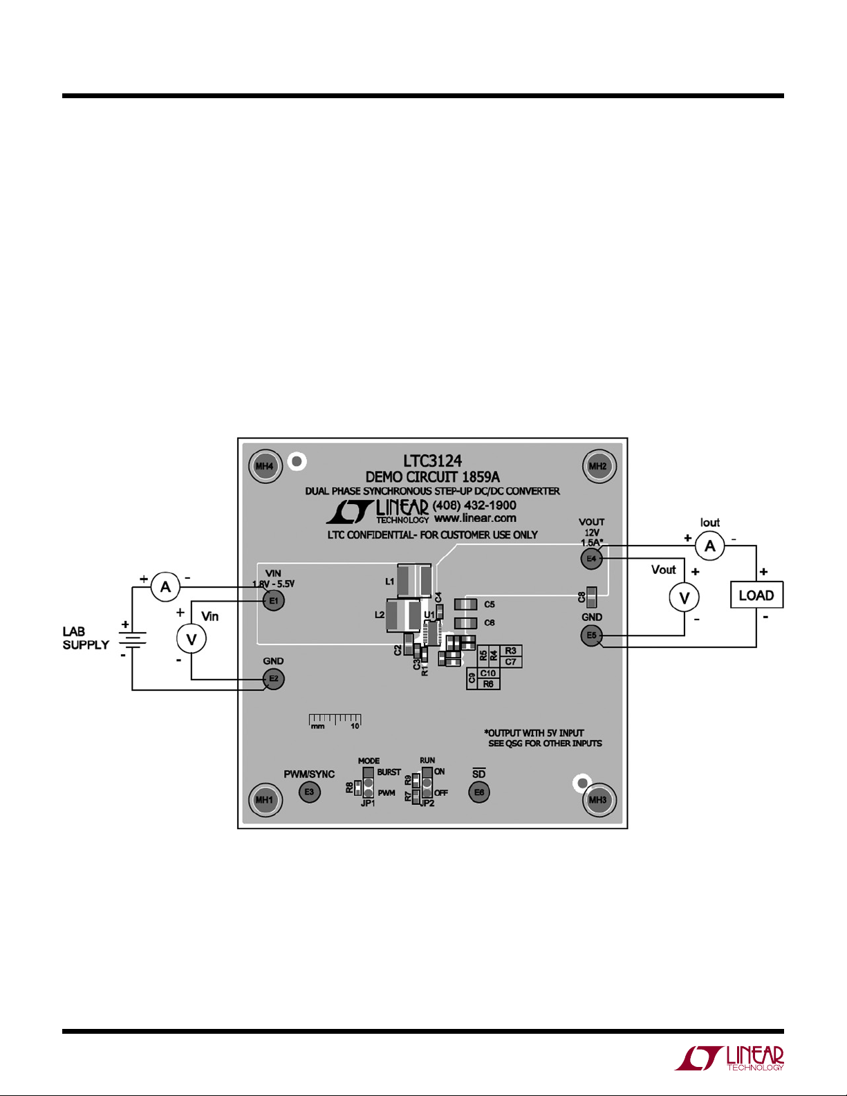
the performance of the LTC3124. For proper measurement equipment
procedure below:
NOTE: When measuring the input or output voltage ripple,
care must be taken to minimize the length of oscilloscope
probe ground lead. Measure the input or output voltage
ripple by connecting the probe tip directly across the VIN
or VOUT and GND terminals as shown in Figure 2.
1. With power off, connect the input power supply to V
and GND.
2. Keep the load set to 0A or disconnected.
setup refer to Figure 1 and follow the
IN
3. Turn the input power source on and slowly increase the
input voltage. Be careful not to exceed 5.5V.
NOTE: Make sure that the input voltage V
exceed 5.5V.
4. Set the input voltage to 5V and check for the proper
output voltage of 12V. If there is no output, temporarily
disconnect the load to make sure that the load is not
set too high.
5. Once the proper output voltage is established, adjust
the load and observe the output voltage regulation,
ripple voltage, efficiency and other parameters.
does not
IN
2
Figure 1. Proper Measurement Equipment Setup
dc1859afa
Page 3
QUICK START PROCEDURE
EFFICIENCY (%)
95
dc1859a F03
10000
DEMO MANUAL DC1859A
+ –
Figure 2. Measuring Input or Output Ripple
C
OUT
V
OUT
Changing the Output Voltage
To change the output voltage from the programmed 12V,
change the voltage divider resistors connected to LTC3124
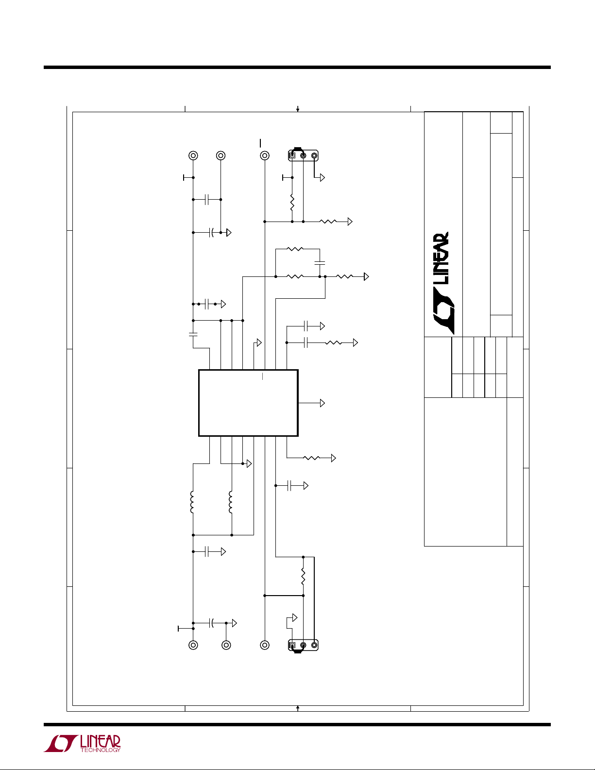
FB pin (see the schematic on page 5).
Converter Output Current
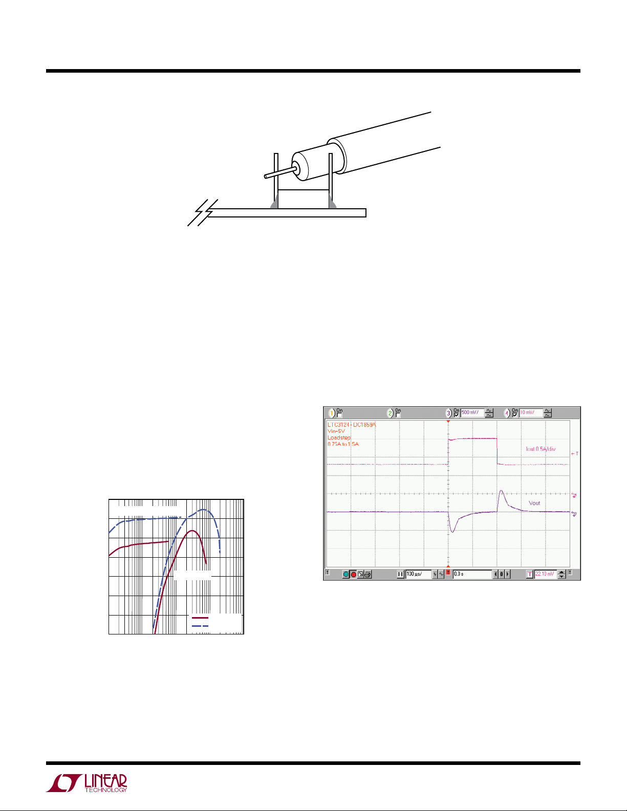
The DC1859 output current capability depends on the
input voltage. Typical performance of DC1859A is shown
in Figure 3. As can be seen from Figure 3, the maximum
output current is 800mA with 2.6V input and 2A with 5V
input. The efficiency is high at light loads thanks to phase
shedding in BURST mode. By disabling one phase the
related switching losses are reduced and the efficiency
is maximized.
GND
Output Load Step Response
The load step response of DC1859A is dependent on the
amount and type of output caps used. If higher load steps
need to be handled more output capacitance can be added
in order to keep the voltage transients at the desired level.
The load step transients are shown in Figure 4. Other types
of low ESR and high value capacitors can
be used if space
is available to reduce load transients to desired level.
Burst Mode OPERATION
90
85
80
PWM MODE
10010
I
(mA)
OUT
VIN = 2.6V
= 5V
V
IN
75
70
65
60
1 1000
Figure 3. The Efficiency Is Maximized for Light Loads by
Shedding One Phase in Burst Mode Operation. The Efficiency Is
Over 90% at Higher Loads and It Reaches 92% at 800mA Load
Figure 4. The LTC3124 Has Excellent Load Step Response with
Small Output Capacitors Thanks to High Switching Frequency
and Fast Feedback Loop Compensation
Start-Up and Soft-Start Function
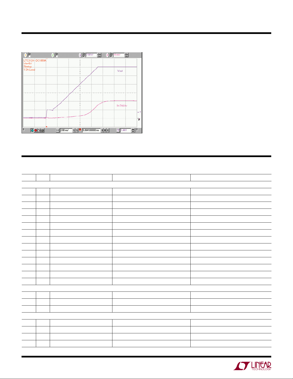
The DC1859 features internal 10ms soft-start circuit that
prevents input current surge at start-up. The soft-start
circuit also prevents output voltage overshoot when output
voltage ramp reaches regulation.
dc1859afa
3
Page 4
DEMO MANUAL DC1859A
QUICK START PROCEDURE
Figure 5. The DC1859 Ramps the Output Slowly at Start-Up
without Generating an Input Current Surge
PARTS LIST
Output Short Circuit Protection
The LTC3124 features safe short-circuit and thermal
protection. The part can operate continuously with output
shorted while maintaining a maximum set current limit. The
peak switch current is reduced during overload to about
2A and is restored to 3.5A once the output exceeds 1.5V.
ITEM QTY REFERENCE PART DESCRIPTION MANUFACTURER/PART NUMBER
Required Circuit Components
2 1 C2 CAP, 0805 10µF 10% 10V X5R MURATA GRM21BR61A106KE19L
3 1 C3 CAP, 0603 4.7µF 10% 10V X5R AVX 0603ZD475K AT2A
4 1 C4 CAP, 0603 0.1µF 10% 25V X7R AVX 06033C104K AT2A
5 2 C5, C6 CAP, 1206 22µF 20% 25V X5R MURATA GRM31CR61E226ME15L
7 1 C8 CAP, 0805 1µF 20% 16V X5R AVX 0805YD105M AT2A
8 1 C9 CAP, 0603 680pF 10% 25V X7R AVX 06033C681K AT2A
9 1 C10 CAP, 0603 56pF 5% 50V C0G AVX 06035A560JAT2A
12 2 L1, L2 IND, 4.7µH COILCRAFT XAL6060-472MEC
14 1 R1 RES, 0603 28k 1% 1/10W VISHAY CRCW060328K0FKEA
16 1 R4 RES, 0603 1M 1% 1/10W VISHAY CRCW06031M00FKEA
17 1 R5 RES. 0603 110k 1% 1/10W VISHAY CRCW0603110KFKEA
18 1 R6 RES, 0603 51.1k 1% 1/10W VISHAY CRCW060351K1FKEA
19 2 R8, R9 RES, 0603 1M 5% 1/10W VISHAY CRCW06031M00JNEA
20 1 U1 IC, DC/DC CONVERTER LINEAR TECH. LTC3124EDHC#PBF
Additional Demo Board Circuit Components
1 0 C1, C11 CAP. 7343 OPTION OPTION
6 0 C7 CAP, 0603 OPTION OPTION
15 0 R3, R7 RES, 0603 OPTION OPTION
Hardware: For Demo Board Only
10 6 E1, E2, E3, E4, E5, E6 TURRET MILL MAX 2501-2-00-80-00-00-07-0
11 2 JP1, JP2 HEADER, 3 PIN SINGLE ROW SULLINS, NRPN031PAEN-RC
13 4 MH1, MH2, MH3, MH4 STANDOFF, SNAP ON KEYSTONE_8831
21 2 JP1, JP2 SHUNT SAMTEC 2SN-BK-G
4
dc1859afa
Page 5
DEMO MANUAL DC1859A
5
5
4
4
3
3
2
2
1
1
11
11
11
SCHEMATIC DIAGRAM
2
2
2
ON
1.5A [1]
12V
12V
C8
C8
C6
C5
0.1uFC40.1uF
1uF
1uF
C11
C11
+
+
22uF
22uF
16
E5
25V
25V
OPT
OPT
25VC522uF
25V
25VC622uF
25V
CAP
GNDE5GND
15
VOUTB
13NC14
VOUTA
E6SDE6
12SD11
SGND
VOUT
VOUT
E4
E4
VOUT
C4
SD
RUN
RUN
VIN
9
10
FB
ON
132
R91MR9
1M
R3
OPTR3OPT
C7
R41M1%R41M
1%
C10
56pF
C10
56pF
C9
680pFC9680pF
VC
17
EXPOSED PAD
OFF
OFF
R7
JP2
JP2
R6
R6
OPTR7OPT
OPTC7OPT
51.1k
51.1k
R5
1%
1%
110k
1%R5110k
1%
www.linear.com
www.linear.com
www.linear.com
Milpitas, CA 95035
Phone: (408)432-1900
Milpitas, CA 95035
Phone: (408)432-1900
Milpitas, CA 95035
Phone: (408)432-1900
Fax: (408)434-0507
Fax: (408)434-0507
Fax: (408)434-0507
1630 McCarthy Blvd.
1630 McCarthy Blvd.
1630 McCarthy Blvd.
LTC CONFIDENTIAL - FOR CUSTOMER USE ONLY
LTC CONFIDENTIAL - FOR CUSTOMER USE ONLY
LTC CONFIDENTIAL - FOR CUSTOMER USE ONLY
TECHNOLOGY
TECHNOLOGY
TECHNOLOGY
MI
MI
MI
APPROVALS
APPROVALS
APPROVALS
PCB DES.
PCB DES.
PCB DES.
DC/DC CONVERTER
DC/DC CONVERTER
DC/DC CONVERTER
DUAL PHASE SYNCHRONOUS STEP-UP
DUAL PHASE SYNCHRONOUS STEP-UP
DUAL PHASE SYNCHRONOUS STEP-UP
SCHEMATIC
SCHEMATIC
SCHEMATIC
TITLE:
TITLE:
TITLE:
GORAN P.
GORAN P.
GORAN P.
APP ENG.
APP ENG.
APP ENG.
SHEET OF
SHEET OF
SHEET OF
LTC3124EDHC
LTC3124EDHC
LTC3124EDHC
DEMO CIRCUIT 1859A
DEMO CIRCUIT 1859A
DEMO CIRCUIT 1859A
Wednesday, June 25, 2014
Wednesday, June 25, 2014
Wednesday, June 25, 2014
IC NO. REV.
IC NO. REV.
IC NO. REV.
N/A
N/A
N/A
SIZE
DATE:
SIZE
DATE:
SIZE
DATE:
SCALE = NONE
SCALE = NONE
SCALE = NONE
PGNDA
SWA
4
3
Coilcraft
Coilcraft
XAL6060-472
XAL6060-472
GNDE2GND
C C
VIN
5
E3
E3
U1
L1
L1
4.7uH
4.7uH
VIN
E1
E1
D D
1
Coilcraft
Coilcraft
XAL6060-472
XAL6060-472
C2
C2
10V
10V
10uF
10uF
(OPT)
(OPT)
C1
C1
+
+
VIN
VIN
1.8V - 5.5V
1.8V - 5.5V
L2
L2
2
E2
4.7uH
4.7uH
PGNDB
SWB
LTC3124EDHC
LTC3124EDHC
U1
PWM/SYNC
VCC
8
6
7
C3
4.7uF
C3
4.7uF
MODE
MODE
PWM/SYNC
PWM/SYNC
RT
132
R1
10V
10V
R81MR8
BURST
BURST
28k
1%R128k
1%
1M
PWM
PWM
JP1
JP1
CUSTOMER NOTICE
CUSTOMER NOTICE
CUSTOMER NOTICE
LINEAR TECHNOLOGY HAS MADE A BEST EFFORT TO DESIGN A
CIRCUIT THAT MEETS CUSTOMER-SUPPLIED SPECIFICATIONS;
HOWEVER, IT REMAINS THE CUSTOMER'S RESPONSIBILITY TO
LINEAR TECHNOLOGY HAS MADE A BEST EFFORT TO DESIGN A
CIRCUIT THAT MEETS CUSTOMER-SUPPLIED SPECIFICATIONS;
HOWEVER, IT REMAINS THE CUSTOMER'S RESPONSIBILITY TO
LINEAR TECHNOLOGY HAS MADE A BEST EFFORT TO DESIGN A
CIRCUIT THAT MEETS CUSTOMER-SUPPLIED SPECIFICATIONS;
HOWEVER, IT REMAINS THE CUSTOMER'S RESPONSIBILITY TO
[1] OUTPUT WITH 5V INPUT. SEE QSG FOR OTHER INPUTS.
NOTE: UNLESS OTHERWISE SPECIFIED,
B B
VERIFY PROPER AND RELIABLE OPERATION IN THE ACTUAL
APPLICATION. COMPONENT SUBSTITUTION AND PRINTED
CIRCUIT BOARD LAYOUT MAY SIGNIFICANTLY AFFECT CIRCUIT
PERFORMANCE OR RELIABILITY. CONTACT LINEAR
TECHNOLOGY APPLICATIONS ENGINEERING FOR ASSISTANCE.
THIS CIRCUIT IS PROPRIETARY TO LINEAR TECHNOLOGY AND
VERIFY PROPER AND RELIABLE OPERATION IN THE ACTUAL
APPLICATION. COMPONENT SUBSTITUTION AND PRINTED
CIRCUIT BOARD LAYOUT MAY SIGNIFICANTLY AFFECT CIRCUIT
PERFORMANCE OR RELIABILITY. CONTACT LINEAR
TECHNOLOGY APPLICATIONS ENGINEERING FOR ASSISTANCE.
VERIFY PROPER AND RELIABLE OPERATION IN THE ACTUAL
APPLICATION. COMPONENT SUBSTITUTION AND PRINTED
CIRCUIT BOARD LAYOUT MAY SIGNIFICANTLY AFFECT CIRCUIT
PERFORMANCE OR RELIABILITY. CONTACT LINEAR
TECHNOLOGY APPLICATIONS ENGINEERING FOR ASSISTANCE.
A A
SUPPLIED FOR USE WITH LINEAR TECHNOLOGY PARTS.
THIS CIRCUIT IS PROPRIETARY TO LINEAR TECHNOLOGY AND
SUPPLIED FOR USE WITH LINEAR TECHNOLOGY PARTS.
THIS CIRCUIT IS PROPRIETARY TO LINEAR TECHNOLOGY AND
SUPPLIED FOR USE WITH LINEAR TECHNOLOGY PARTS.
dc1859afa
Information furnished by Linear Technology Corporation is believed to be accurate and reliable.
However, no responsibility is assumed for its use. Linear Technology Corporation makes no representation that the interconnection of its circuits as described herein will not infringe on existing patent rights.
5
Page 6

DEMO MANUAL DC1859A
DEMONSTRATION BOARD IMPORTANT NOTICE
Linear Technology Corporation (LT C ) provides the enclosed product(s) under the following AS IS conditions:
This demonstration board (DEMO BOARD) kit being sold or provided by Linear Technology is intended for use for ENGINEERING DEVELOPMENT
OR EVALUATION PURPOSES ONLY and is not provided by LT C for commercial use. As such, the DEMO BOARD herein may not be complete
in terms of required design-, marketing-, and/or manufacturing-related protective considerations, including but not limited to product safety
measures typically found in finished commercial goods. As a prototype, this product does not fall within the scope of the European Union
directive on electromagnetic compatibility and therefore may or may not meet the technical requirements of the directive, or other regulations.
If this evaluation kit does not meet the specifications recited in the DEMO BOARD manual the kit may be returned within 30 days from the date
of delivery for a full refund. THE FOREGOING WARRANTY IS THE EXCLUSIVE WARRANTY MADE BY THE SELLER TO BUYER AND IS IN LIEU
OF ALL OTHER WARRANTIES, EXPRESSED, IMPLIED, OR STATUTORY, INCLUDING ANY WARRANTY OF MERCHANTABILITY OR FITNESS
FOR ANY PARTICULAR PURPOSE. EXCEPT TO THE EXTENT OF THIS INDEMNITY, NEITHER PARTY SHALL BE LIABLE TO THE OTHER FOR
ANY INDIRECT, SPECIAL, INCIDENTAL, OR CONSEQUENTIAL DAMAGES.
The user assumes all responsibility and liability for proper and safe handling of the goods. Further, the user releases LT C from all claims
arising from the handling or use of the goods. Due to the open construction of the product, it is the user’s responsibility to take any and all
appropriate precautions with regard to electrostatic discharge. Also be aware that the products herein may not be regulatory compliant or
agency certified (FCC, UL, CE, etc.).
No License is granted under any patent right or other intellectual property whatsoever. LT C assumes no liability for applications assistance,
customer product design, software performance, or infringement of patents or any other intellectual property rights of any kind.
LT C currently services a variety of customers for products around the world, and therefore this transaction is not exclusive.
Please read the DEMO BOARD manual prior to handling the product. Persons handling this product must have electronics training and
observe good laboratory practice standards. Common sense is encouraged.
This notice contains important safety information about temperatures and voltages. For further safety concerns, please contact a LT C application engineer.
Mailing Address:
Linear Technology
1630 McCarthy Blvd.
Milpitas, CA 95035
Copyright © 2004, Linear Technology Corporation
6
Linear Technology Corporation
1630 McCarthy Blvd., Milpitas, CA 95035-7417
(408) 432-1900 ● FAX: (408) 434-0507 ● www.linear.com
dc1859afa
LT 1014 REV A • PRINTED IN USA
LINEAR TECHNOLOGY CORPORATION 2014
 Loading...