

Page 1
LTC2914
1
2914fa
Quad UV/OV
Positive/Negative
Voltage Monitor
n
Desktop and Notebook Computers
n
Network Servers
n
Core, I/O Voltage Monitors
n
Monitors Four Voltages Simultaneously
n
Adjustable UV and OV Trip Values
n
Guaranteed Threshold Accuracy: ±1.5% of
Monitored Voltage over Temperature
n
Input Glitch Rejection
n
Monitors up to Two Negative Voltages
n
Buffered 1V Reference Output
n
Adjustable Reset Timeout with Timeout Disable
n
62μA Quiescent Current
n
Open-Drain OV and UV Outputs
n
Guaranteed OV and UV for VCC ≥ 1V
n
Available in 16-Lead SSOP and 16-Lead
(5mm × 3mm) DFN Packages
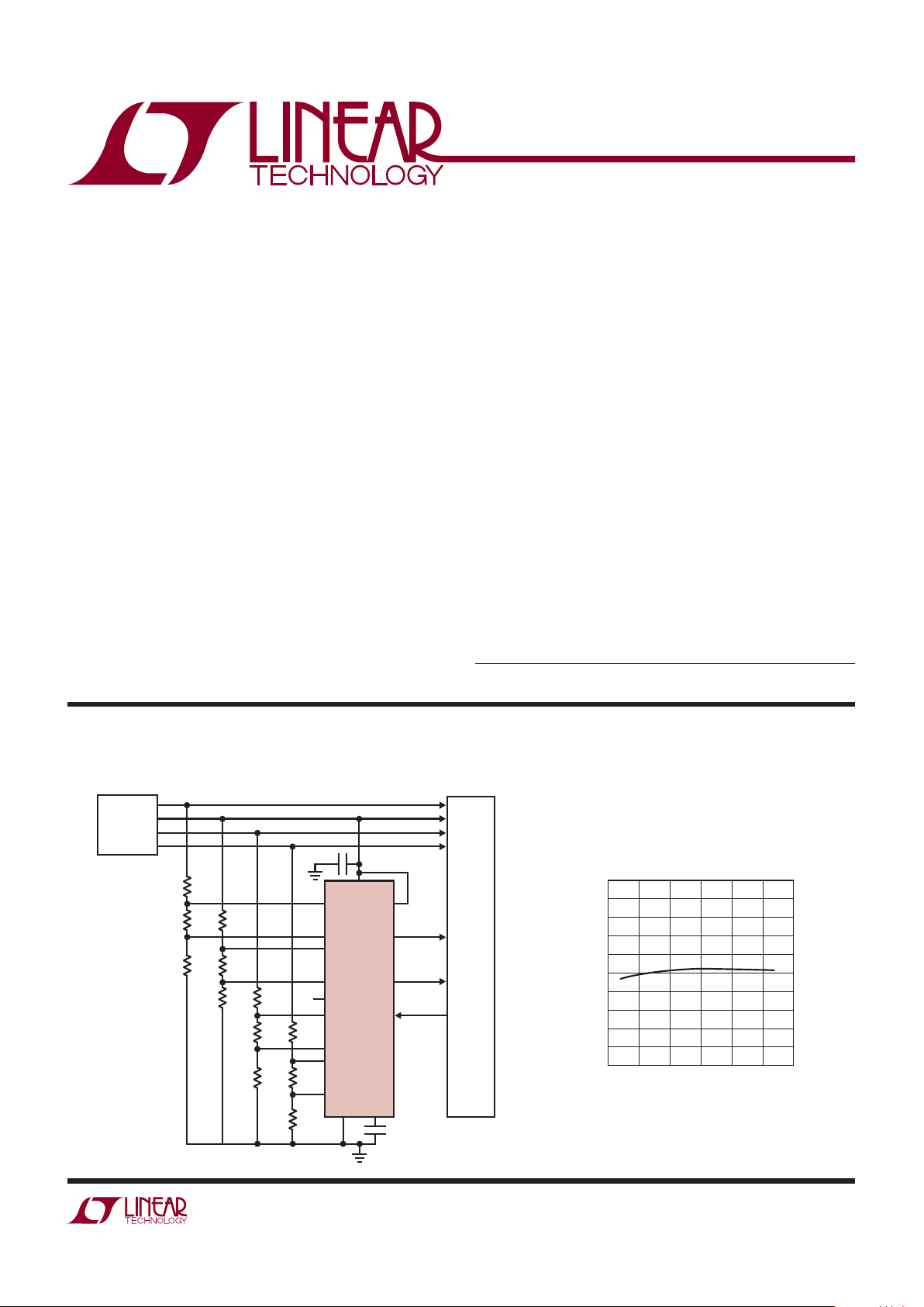
Quad UV/OV Supply Monitor,10% Tolerance, 5V, 3.3V, 2.5V, 1.8V
The LTC®2914 is a quad input voltage monitor intended for
monitoring multiple voltages in a variety of applications.
Dual inputs for each monitored voltage allow monitoring
four separate undervoltage (UV) conditions and four
separate overvoltage (OV) conditions. All monitors share a
common undervoltage output and a common overvoltage
output. The LTC2914-1 has latching capability for the
overvoltage output. The LTC2914-2 has functionality to
disable both the overvoltage and undervoltage outputs.
Polarity selection and a buffered reference allow monitoring
up to two separate negative voltages. A three-state input pin
allows setting the polarity of two inputs without requiring
any external components. Glitch fi ltering ensures reliable
reset operation without false or noisy triggering.
The LTC2914 provides a precise, versatile, space-conscious, micropower solution for voltage monitoring.
Input Threshold Voltage
vs Temperature
TYPICAL APPLICATION
FEATURES
APPLICATIONS
DESCRIPTION
L, LT, LTC and LTM are registered trademarks of Linear Technology Corporation.
All other trademarks are the property of their respective owners.
VH1
V
CC
LTC2914-1
SYSTEM
2914 TA01a
0.1μF
GND TMR
VL1
VL2
VH2
REF
VL3
VH3
OV
UV
LATCH
SEL
VL4
C
TMR
22nF
TIMEOUT = 200ms
VH4
1k
4.53k
4.53k
12.4k1k
19.6k4.53k
27.4k1k
44.2k
5V
3.3V
2.5V
1.8V
1k
4.53k
P0WER
SUPPLIES
TEMPERATURE (°C)
–50
0.495
THRESHOLD VOLTAGE, V
OUT
(V)
0.497
0.499
0.501
–25
0
25 50
2914 TA01b
75
0.503
0.505
0.496
0.498
0.500
0.502
0.504
100
Page 2
LTC2914
2
2914fa
Terminal Voltages
V
CC
(Note 3) ............................................. –0.3V to 6V
OV, UV ................................................... –0.3V to 16V
TMR ..........................................–0.3V to (V
CC
+ 0.3V)
VLn, VHn, LATCH, DIS, SEL .................. –0.3V to 7.5V
Terminal Currents
I
VCC
....................................................................10mA
Reference Load Current (I
REF
) ...........................±1mA
I
UV
, IOV ...............................................................10mA
(Notes 1, 2)
16
15
14
13
12
11
10
9
17
1
2
3
4
5
6
7
8
V
CC
TMR
SEL
LATCH
UV
OV
REF
GND
VH1
VL1
VH2
VL2
VH3
VL3
VH4
VL4
TOP VIEW
DHC PACKAGE
16-LEAD (5mm × 3mm) PLASTIC DFN
T
JMAX
= 150°C, θJA = 43.5°C/W
EXPOSED PAD (PIN 17)
PCB GND CONNECTION OPTIONAL
GN PACKAGE
16-LEAD PLASTIC SSOP
1
2
3
4
5
6
7
8
TOP VIEW
16
15
14
13
12
11
10
9
VH1
VL1
VH2
VL2
VH3
VL3
VH4
VL4
V
CC
TMR
SEL
LATCH
UV
OV
REF
GND
T
JMAX
= 150°C, θJA = 110°C/W
ORDER PART
NUMBER
DHC PART
MARKING*
LTC2914CDHC-1
LTC2914IDHC-1
LTC2914HDHC-1
29141
29141
29141
ORDER PART
NUMBER
GN PART
MARKING
LTC2914CGN-1
LTC2914IGN-1
LTC2914HGN-1
29141
2914I1
2914H1
16
15
14
13
12
11
10
9
17
1
2
3
4
5
6
7
8
V
CC
TMR
SEL
DIS
UV
OV
REF
GND
VH1
VL1
VH2
VL2
VH3
VL3
VH4
VL4
TOP VIEW
DHC PACKAGE
16-LEAD (5mm × 3mm) PLASTIC DFN
T
JMAX
= 150°C, θJA = 43.5°C/W
EXPOSED PAD (PIN 17)
PCB GND CONNECTION OPTIONAL
GN PACKAGE
16-LEAD PLASTIC SSOP
1
2
3
4
5
6
7
8
TOP VIEW
16
15
14
13
12
11
10
9
VH1
VL1
VH2
VL2
VH3
VL3
VH4
VL4
V
CC
TMR
SEL
DIS
UV
OV
REF
GND
T
JMAX
= 150°C, θJA = 110°C/W
ORDER PART
NUMBER
DHC PART
MARKING*
LTC2914CDHC-2
LTC2914IDHC-2
LTC2914HDHC-2
29142
29142
29142
ORDER PART
NUMBER
GN PART
MARKING
LTC2914CGN-2
LTC2914IGN-2
LTC2914HGN-2
29142
2914I2
2914H2
Order Options Tape and Reel: Add #TR
Lead Free: Add #PBF Lead Free Tape and Reel: Add #TRPBF
Lead Free Part Marking: http://www.linear.com/leadfree/
*The temperature grade is identifi ed by a label on the shipping container.
Operating Temperature Range
LTC2914C ................................................0°C to 70°C
LTC2914I.............................................. –40°C to 85°C
LTC2914H .......................................... –40°C to 125°C
Storage Temperature Range ................... –65°C to 150°C
Lead Temperature (Soldering, 10 sec)
SSOP ................................................................ 300°C
ABSOLUTE MAXIMUM RATINGS
PACKAGE/ORDER INFORMATION
Page 3
LTC2914
3
2914fa
The l denotes the specifi cations which apply over the full operating
temperature range, otherwise specifi cations are at T
A
= 25°C. VCC = 3.3V, VLn = 0.45V, VHn = 0.55V, LATCH = VCC, SEL = VCC,
DIS = Open unless otherwise noted. (Note 2)
SYMBOL PARAMETER CONDITIONS MIN TYP MAX UNITS
V
SHUNT
VCC Shunt Regulator Voltage ICC = 5mA
l
6.2 6.6 6.9 V
–40ºC < T
A
< 125ºC
l
6.2 6.6 7.0 V
ΔV
SHUNT
VCC Shunt Regulator Load Regulation ICC = 2mA to 10mA
l
200 300 mV
V
CC
Supply Voltage (Note 3)
l
2.3 V
SHUNT
V
V
CCR(MIN)
Minimum VCC Output Valid DIS = 0V
l
1V
V
CC(UVLO)
Supply Undervoltage Lockout VCC Rising, DIS = 0V
l
1.9 2 2.1 V
ΔV
CC(UVHYST)
Supply Undervoltage Lockout Hysteresis DIS = 0V
l
52550 mV
I
CC
Supply Current VCC = 2.3V to 6V
l
62 100 μA
V
REF
Reference Output Voltage I
VREF
= ±1mA
l
0.985 1 1.015 V
–40ºC < T
A
< 125ºC
l
0.985 1 1.020 V
V
UOT
Undervoltage/Overvoltage Voltage Threshold
l
492 500 508 mV
t
UOD
Undervoltage/Overvoltage Voltage Threshold
to Output Delay
VHn = V
UOT
– 5mV or VLn = V
UOT
+ 5mV
l
50 125 500 μs
I
VHL
VHn, VLn Input Current
l
±15 nA
–40ºC < T
A
< 125ºC
l
±30 nA
t
UOTO
UV/OV Time-Out Period C
TMR
= 1nF
l
6 8.5 12.5 ms
–40ºC < T
A
< 125ºC
l
6 8.5 14 ms
V
LATCH(IH)
OV Latch Clear Input High
l
1.2 V
V
LATCH(IL)
OV Latch Clear Threshold Input Low
l
0.8 V
I
LATCH
LATCH Input Current V
LATCH
> 0.5V
l
±1 μA
V
DIS(IH)
DIS Input High
l
1.2 V
V
DIS(IL)
DIS Input Low
l
0.8 V
I
DIS
DIS Input Current V
DIS
> 0.5V
l
123 μA
I
TMR(UP)
TMR Pull-Up Current V
TMR
= 0V
l
–1.3 –2.1 –2.8 μA
–40ºC < T
A
< 125ºC
l
–1.2 –2.1 –2.8 μA
I
TMR(DOWN)
TMR Pull-Down Current V
TMR
= 1.6V
l
1.3 2.1 2.8 μA
–40ºC < T
A
< 125ºC
l
1.2 2.1 2.8 μA
V
TMR(DIS)
Timer Disable Voltage Referenced to V
CC
l
–180 –270 mV
V
OH
Output Voltage High UV/OV VCC = 2.3V, I
UV/OV
= –1μA
l
1V
V
OL
Output Voltage Low UV/OV VCC = 2.3V, I
UV/OV
= 2.5mA
V
CC
= 1V, IUV = 100μA
l
l
0.1
0.01
0.3
0.15
V
V
Three-State Input SEL
V
IL
Low Level Input Voltage
l
0.4 V
V
IH
High Level Input Voltage
l
1.4 V
V
Z
Pin Voltage when Left in Hi-Z State I
SEL
= ±10μA
l
0.7 0.9 1.1 V
–40ºC < T
A
< 125ºC
l
0.6 0.9 1.2 V
I
SEL
SEL High, Low Input Current
l
±25 μA
I
SEL(MAX)
Maximum SEL Input Current SEL Tied to Either VCC or GND
l
±30 μA
ELECTRICAL CHARACTERISTICS
Page 4
LTC2914
4
2914fa
Input Threshold Voltage
vs Temperature
Supply Current vs Temperature
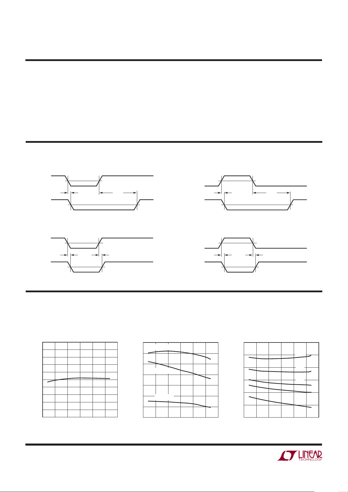
VCC Shunt Voltage
vs Temperature
VHn Monitor Timing VLn Monitor Timing
VHn Monitor Timing (TMR Pin Strapped to VCC) VLn Monitor Timing (TMR Pin Strapped to VCC)
NOTE: WHEN AN INPUT IS CONFIGURED AS A NEGATIVE SUPPLY MONITOR, VHn WILL TRIGGER AN OV CONDITION AND VLn WILL TRIGGER A UV CONDITION
Specifi cations are at TA = 25°C, VCC = 3.3V unless otherwise noted.
Note 1: Stresses beyond those listed under Absolute Maximum Ratings
may cause permanent damage to the device. Exposure to any Absolute
Maximum Rating condition for extended periods may affect device
reliability and lifetime.
Note 2: All currents into pins are positive; all voltages are referenced to
GND unless otherwise noted.
Note 3: VCC maximum pin voltage is limited by input current. Since the
V
CC
pin has an internal 6.5V shunt regulator, a low impedance supply that
exceeds 6V may exceed the rated terminal current. Operation from higher
voltage supplies requires a series dropping resistor. See Applications
Information.
ELECTRICAL CHARACTERISTICS
TIIMING DIAGRAMS
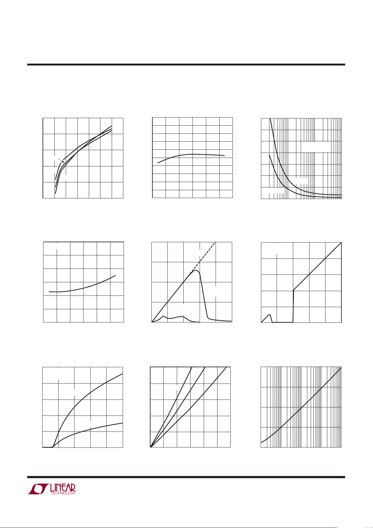
TYPICAL PERFORMANCE CHARACTERISTICS
VHn
UV
V
UOT
1V
t
UOD
t
UOTO
2914 TD01
VLn
OV
V
UOT
1V
t
UOD
t
UOTO
2914 TD02
VHn
UV
V
UOT
1V
t
UOD
t
UOD
2914 TD03
VLn
OV
V
UOT
1V
t
UOD
t
UOD
2914 TD04
TEMPERATURE (°C)
–50
0.495
THRESHOLD VOLTAGE, V
OUT
(V)
0.497
0.499
0.501
–25
0
25 50
2914 G01
75
0.503
0.505
0.496
0.498
0.500
0.502
0.504
100
TEMPERATURE (°C)
–50 50 75–25 25
40
I
CC
(μA)
50
55
45
60
0
2914 G02
100
75
70
65
VCC = 5V
VCC = 3.3V
VCC = 2.3V
TEMPERATURE (°C)
–50
6.2
V
CC
(V)
6.3
6.4
6.5
6.6
6.8
–25
02550
2914 G03
75 100
6.7
200μA
1mA
2mA
5mA
10mA
Page 5
LTC2914
5
2914fa
VCC Shunt Voltage vs I
CC
Buffered Reference Voltage
vs Temperature
Transient Duration
vs Comparator Overdrive
UV Output Voltage vs V
CC
UV/OV Voltage Output Low
vs Output Sink Current
Reset Timeout Period
vs CapacitanceUV, I
SINK
vs V
CC
Reset Timeout Period
vs Temperature
UV Output Voltage vs V
CC
Specifi cations are at TA = 25°C, VCC = 3.3V unless otherwise noted.
TYPICAL PERFORMANCE CHARACTERISTICS
ICC (mA)
–2 0
6.25
V
CC
(V)
6.45
6.75
2
6
8
2914 G04
6.35
6.65
6.55
4
10
12
25°C
–40°C
85°C
TEMPERATURE (°C)
–50
0.995
REFERENCE VOLTAGE, V
REF
(V)
0.997
0.999
1.001
–25
0
25 50
2914 G05
75
1.003
1.005
0.996
0.998
1.000
1.002
1.004
100
COMPARATOR OVERDRIVE PAST THRESHOLD (%)
0.1
400
TYPICAL TRANSIENT DURATION (μs)
500
600
700
1 10 100
2914 G06
300
200
100
0
VCC = 6V
RESET OCCURS
ABOVE CURVE
VCC = 2.3V
TEMPERATURE (°C)
–50
6
UV/OV TIMEOUT PERIOD, t
UOTO
(ms)
7
8
9
10
12
–25
02550
2914 G07
75 100
11
C
TMR
= 1nF
SUPPLY VOLTAGE, VCC (V)
0
UV VOLTAGE (V)
0.4
0.6
0.8
2914 G08
0.2
0
0.2
0.4
0.6
1.0
0.8
V
CC
UV WITH
10k PULL-UP
UV WITHOUT
10k PULL-UP
SUPPLY VOLTAGE, VCC (V)
0
UV VOLTAGE (V)
3
4
5
4
2914 G09
2
1
0
1
2
3
5
VHn = 0.55V
SEL = V
CC
SUPPLY VOLTAGE, VCC (V)
0
PULL-DOWN CURRENT, I
UV
(mA)
3
4
5
4
2914 G10
2
1
0
1
2
3
5
VHn = 0.45V
SEL = V
CC
UV AT 150mV
UV AT 50mV
I
UV/OV
(mA)
0
0
UV/OV, V
OL
(V)
0.2
0.4
0.6
0.8
1.0
5
10 15 20
2914 G11
25 30
85°C
–40°C
25°C
TMR PIN CAPACITANCE, C
TMR
(nF)
10
UV/OV TIMEOUT PERIOD, t
UOTO
(ms)
100
1000
10000
0.1 10 100 1000
2914 G12
1
1
Page 6

LTC2914
6
2914fa
DIS (Pin 13, LTC2914-2): Output Disable Input. Disables
the OV and UV output pins. When DIS is pulled high, the
OV and UV pins are not asserted except during a UVLO
condition. Pin has a weak (2μA) internal pull-down to GND.
Leave pin open if unused.
Exposed Pad (Pin 17, DFN Package): Exposed Pad may
be left open or connected to device ground.
GND (Pin 9): Device Ground
LATCH (Pin 13, LTC2914-1): OV Latch Clear/Bypass Input.
When pulled low, OV is latched when asserted. When
pulled high, OV latch is cleared. While held high, OV has
the same delay and output characteristics as UV.
OV (Pin 11): Overvoltage Logic Output. Asserts low when
any positive polarity input voltage is above threshold or
any negative polarity input voltage is below threshold.
Latched low (LTC2914-1). Held low for an adjustable
delay time after all inputs are valid (LTC2914-2). Pin has
a weak pull-up to V
CC
and may be pulled above VCC using
an external pull-up. Leave pin open if unused.
REF (Pin 10): Buffered Reference Output. 1V reference
used for the offset of negative-monitoring applications.
The buffered reference sources and sinks up to 1mA. The
reference drives capacitive loads up to 1nF. Larger capacitive
loads may cause instability. Leave pin open if unused.
SEL (Pin 14): Input Polarity Select Three-State Input.
Connect to V
CC
, GND or leave unconnected in open state
to select one of three possible input polarity combinations
(refer to Table 1).
T
MR (Pin 15): Reset Delay Timer. Attach an external
capacitor (C
TMR
) of at least 10pF to GND to set a reset
delay time of 9ms/nF. A 1nF capacitor will generate an
8.5ms reset delay time. Tie pin to V
CC
to bypass timer.
UV (Pin 12): Undervoltage Logic Output. Asserts low when
any positive polarity input voltage is below threshold or
any negative polarity input voltage is above threshold.
Held low for an adjustable delay time after all voltage
inputs are valid. Pin has a weak pull-up to V
CC
and may
be pulled above V
CC
using an external pull-up. Leave pin
open if unused.
V
CC
(Pin 16): Supply Voltage. Bypass this pin to GND with
a 0.1μF (or greater) capacitor. Operates as a direct supply
input for voltages up to 6V. Operates as a shunt regulator for
supply voltages greater than 6V and must have a resistance
between the pin and the supply to limit input current to no
greater than 10mA. When used without a current-limiting
resistance, pin voltage must not exceed 6V.
VH1/VH2 (Pin 1/Pin 3): Voltage High Inputs 1 and 2. When
the voltage on this pin is below 0.5V, an undervoltage
condition is triggered. Tie pin to V
CC
if unused.
VH3/VH4 (Pin 5/Pin 7): Voltage High Inputs 3 and 4. The
polarity of the input is selected by the state of the SEL pin
(refer to Table 1). When the monitored input is confi gured
as a positive voltage, an undervoltage condition is triggered when the pin is below 0.5V. When the monitored
input is confi gured as a negative voltage, an overvoltage
condition is triggered when the pin is below 0.5V. Tie pin
to V
CC
if unused.
VL1/VL2 (Pin 2/Pin 4): Voltage Low Inputs 1 and 2. When
the voltage on this pin is above 0.5V, an overvoltage condition is triggered. Tie pin to GND if unused.
VL3/VL4 (Pin 6/Pin 8): Voltage Low Inputs 3 and 4. The
polarity of the input is selected by the state of the SEL pin
(refer to Table 1). When the monitored input is confi gured
as a positive voltage, an overvoltage condition is triggered
when the pin is above 0.5V. When the monitored input is
confi gured as a negative voltage, an undervoltage condition is triggered when the pin is above 0.5V. Tie pin to
GND if unused.
PIN FUNCTIONS
Page 7

LTC2914
7
2914fa
BLOCK DIAGRAM
8
+
–
+
–
VL4
10
REF
1V
0.5V
BUFFER
SEL
7
VH4
6
+
–
+
–
VL3
+
–
4
VL2
3
+
–
VH2
+
–
2
VL1
1
+
–
VH1
5
VH3
+
–
UVLO
UVLO
2V
V
CC
+
–
1V
LTC2914-1
LTC2914-2
V
CC
THREE-STATE
POLARITY
DECODER
OV PULSE
GENERATOR
DISABLE
OV LATCH
CLEAR/BYPASS
14
TMRV
CC
15
OV
11
LATCH
13
GND
2914 -1 BD
9
16
UV PULSE
GENERATOR
OSCILLATOR
V
CC
400k
UV
12
400k
+
–
1V
DIS
13
2μA
Page 8

LTC2914
8
2914fa
Voltage Monitoring
The LTC2914 is a low power quad voltage monitoring circuit with four undervoltage and four overvoltage inputs. A
timeout period that holds OV or UV asserted after all faults
have cleared is adjustable using an external capacitor and
is externally disabled.
Each voltage monitor has two inputs (VHn and VLn) for
detecting undervoltage and overvoltage conditions. When
confi gured to monitor a positive voltage V
n
using the
3-resistor circuit confi guration shown in Figure 1, V Hn is
connected to the high-side tap of the resistive divider and
VLn is connected to the low-side tap of the resistive divider.
If an input is confi gured as a negative voltage monitor, the
outputs UV
n
and OVn in Figure 1 are swapped internally. Vn
is then connected as shown in Figure 2. Note, VHn is still
connected to the high-side tap and VLn is still connected
to the low-side tap.
Polarity Selection
The three-state polarity-select pin (SEL) selects one of three
possible polarity combinations for the input thresholds,
as described in Table 1. When an input is confi gured for
negative supply monitoring, VHn is confi gured to trigger an
overvoltage condition and VLn is confi gured to trigger an
undervoltage condition. With this confi guration, an OV condition occurs when the supply voltage is more negative than
the confi gured threshold and a UV condition occurs when
the voltage is less negative than the confi gured threshold.
The three-state input pin SEL is connected to GND, VCC or
left unconnected during normal operation. When the pin
is left unconnected, the maximum leakage allowed from
the pin is ±10μA to ensure it remains in the open state.
Table 1 shows the three possible selections of polarity
based on the SEL pin connection.
Table 1. Voltage Polarity Programming (V
UOT
= 0.5V Typical)
SEL V3 INPUT V4 INPUT
V
CC
Positive
VH3 < V
UOT
→ UV
VL3 > V
UOT
→ OV
Positive
VH4 < V
UOT
→ UV
VL4 > V
UOT
→ OV
Open Positive
VH3 < V
UOT
→ UV
VL3 > V
UOT
→ OV
Negative
VH4 < V
UOT
→ OV
VL4 > V
UOT
→ UV
GND Negative
VH3 < V
UOT
→ OV
VL3 > V
UOT
→ UV
Negative
VH4 < V
UOT
→ OV
VL4 > V
UOT
→ UV
3-Step Design Procedure
The following 3-step design procedure allows selecting
appropriate resistances to obtain the desired UV and OV trip
points for the positive voltage monitor circuit in Figure 1
and the negative voltage monitor circuit in Figure 2.
Figure 1. 3-Resistor Positive UV/OV Monitoring Confi guration Figure 2. 3-Resistor Negative UV/OV Monitoring Confi guration
APPLICATIONS INFORMATION
–
+
–
+
+
–
0.5V
LTC2914
UV
n
VHn
R
C
R
B
R
A
2914 F01
V
n
VLn
OV
n
–
+
–
+
+
–
+
–
0.5V
1V
LTC2914
UV
n
VHn
REF
R
A
R
B
R
C
2914 F02
VLn
V
n
OV
n
–
+
Page 9

LTC2914
9
2914fa
For positive supply monitoring, Vn is the desired nominal
operating voltage, I
n
is the desired nominal current through
the resistive divider, V
OV
is the desired overvoltage trip
point and V
UV
is the desired undervoltage trip point.
For negative supply monitoring, to compensate for the 1V
reference, 1V must be subtracted from V
n
, VOV and VUV
before using each in the following equations.
1. Choose R
A
to obtain the desired OV trip point
R
A
is chosen to set the desired trip point for the
overvoltage monitor.
RA=
0.5V
I
n
•
V
n
V
OV
(1)
2. Choose R
B
to obtain the desired UV trip point
Once R
A
is known, RB is chosen to set the desired trip
point for the undervoltage monitor.
RB=
0.5V
I
n
•
V
n
V
UV
–R
A
(2)
3. Choose R
C
to Complete the Design
Once R
A
and RB are known, RC is determined by:
RC=
V
n
I
n
–RA–R
B
(3)
If any of the variables V
n
, In, VUV or VOV change, then each
step must be recalculated.
Positive Voltage Monitor Example
A positive voltage monitor application is shown in Figure 3.
The monitored voltage is a 5V ±10% supply. Nominal current in the resistive divider is 10μA.
1. Find RA to set the OV trip point of the monitor.
RA=
0.5V
10µA
•
5V
5.5V
45.3k
2. Find RB to set the UV trip point of the monitor.
RB=
0.5V
10µA
•
5V
4.5V
– 45.3k 10.2k
3. Determine RC to complete the design.
RC=
5V
10µA
– 45.3k 10.2k 442k
Negative Voltage Monitor Example
A negative voltage monitor application is shown in Figure 4.
The monitored voltage is a –5V ±10% supply. Nominal
current in the resistive divider is 10μA. For the negative
case, 1V is subtracted from V
n
, VOV and VUV.
1. Find RA to set the OV trip point of the monitor.
RA=
0.5V
10µA
•
–5V –1V
–5.5V –1V
46.4k
2. Find RB to set the UV trip point of the monitor.
RB=
0.5V
10µA
•
5V – 1V
4.5V –1V
46.4k 8.45k
3. Determine RC to complete the design.
RC=
–5V –1V
10µA
46.4k 8.45k 549k
Figure 3. Positive Supply Monitor
Figure 4. Negative Supply Monitor
APPLICATIONS INFORMATION
VH1
R
C
442k
R
B
10.2k
R
A
45.3k
V
CC
GND
LTC2914
VL1
2914 F03
OV
UV
SEL
V
CC
5V
V1
5V ±10%
REF
R
A
46.4k
R
B
8.45k
R
C
549k
V
CC
GND
V3
–5V ±10%
LTC2914
VH3
VL3
2914 F04
OV
UV
SEL
V
CC
5V
Page 10

LTC2914
10
2914fa
Power-Up/Power-Down
As soon as V
CC
reaches 1V during power-up, the UV output
asserts low and the OV output weakly pulls to V
CC
.
The LTC2914 is guaranteed to assert UV low and OV high
under conditions of low V
CC
, down to VCC = 1V. Above VCC =
2V (2.1V maximum) the VH and VL inputs take control.
Once all VH inputs and V
CC
become valid an internal timer
is started. After an adjustable delay time, UV weakly pulls
high.
Threshold Accuracy
Reset threshold accuracy is important in a supply-sensitive
system. Ideally, such a system resets only if supply voltages
fall outside the exact thresholds for a specifi ed margin.
All LTC2914 inputs have a relative threshold accuracy of
±1.5% over the full operating temperature range.
For example, when the LTC2914 is programmed to monitor a 5V input with a 10% tolerance, the desired UV trip
point is 4.5V. Because of the ±1.5% relative accuracy of
the LTC2914, the UV trip point is between 4.433V and
4.567V which is 4.5V ±1.5%.
Likewise, the accuracy of the resistances chosen for R
A
,
R
B
and RC affect the UV and OV trip points as well. Using the example just given, if the resistances used to set
the UV trip point have 1% accuracy, the UV trip range is
between 4.354V and 4.650V. This is illustrated in the following calculations.
The UV trip point is given as:
VUV= 0.5V 1+
R
C
RA+ R
B
The two extreme conditions, with a relative accuracy of
1.5% and resistance accuracy of 1%, result in:
V
UV(MIN)
= 0.5V •0.985 • 1+
RC• 0.99
RA+ R
B
()
• 1.01
and
V
UV(MAX)
= 0.5V •1.015 • 1+
RC• 1.01
RA+ R
B
()
• 0.99
For a desired trip point of 4.5V,
R
C
RA+ R
B
= 8
Therefore,
V
UV(MIN)
= 0.5V •0.985 • 1+ 8
0.99
1.01
= 4.354V
and
V
UV(MAX)
= 0.5V •1.015 • 1+ 8
1.01
0.99
= 4.650V
Glitch Immunity
In any supervisory application, noise riding on the monitored DC voltage causes spurious resets. To solve this
problem without adding hysteresis, which causes a new
error term in the trip voltage, the LTC2914 lowpass fi lters
the output of the fi rst stage comparator at each input. This
fi lter integrates the output of the comparator before asserting the UV or OV logic. A transient at the input of the
comparator of suffi cient magnitude and duration triggers
the output logic. The Typical Performance Characteristics
section shows a graph of the Transient Duration vs Comparator Overdrive.
APPLICATIONS INFORMATION
Page 11

LTC2914
11
2914fa
UV/OV Timing
The LTC2914 has an adjustable timeout period (t
UOTO
) that
holds OV or UV asserted after all faults have cleared. This
assures a minimum reset pulse width allowing a settling
time delay for the monitored voltage after it has entered
the valid region of operation.
When any VH input drops below its designed threshold,
the UV pin asserts low. When all inputs recover above
their designed thresholds, the UV output timer starts. If
all inputs remain above their designed thresholds when
the timer fi nishes, the UV pin weakly pulls high. However,
if any input falls below its designed threshold during this
time-out period, the timer resets and restarts when all inputs
are above the designed thresholds. The OV output behaves
as the UV output when LATCH is high (LTC2914-1).
Selecting the UV/OV Timing Capacitor
The UV and OV timeout period (t
UOTO
) for the LTC2914
is adjustable to accommodate a variety of applications.
Connecting a capacitor, C
TMR
, between the TMR pin and
ground sets the timeout period. The value of capacitor
needed for a particular timeout period is:
C
TMR
= t
UOTO
• 115 • 10–9 (F/s)
The Reset Timeout Period vs Capacitance graph found in
the Typical Performance Characteristics shows the desired
delay time as a function of the value of the timer capacitor
that must be used. The TMR pin must have a minimum of
10pF or be tied to V
CC
. For long timeout periods, the only
limitation is the availability of a large value capacitor with
low leakage. Capacitor leakage current must not exceed
the minimum TMR charging current of 1.3μA. Tying the
TMR pin to V
CC
bypasses the timeout period.
Undervoltage Lockout
When V
CC
falls below 2V, the LTC2914 asserts an
undervoltage lockout (UVLO) condition. During UVLO,
UV is asserted and pulled low while OV is cleared and
blocked from asserting. When V
CC
rises above 2V, UV
follows the same timing procedure as an undervoltage
condition on any input.
Shunt Regulator
The LTC2914 has an internal shunt regulator. The V
CC
pin
operates as a direct supply input for voltages up to 6V.
Under this condition, the quiescent current of the device
remains below a maximum of 100μA. For V
CC
voltages
higher than 6V, the device operates as a shunt regulator
and must have a resistance R
Z
between the supply and the
V
CC
pin to limit the current to no greater than 10mA.
When choosing this resistance value, choose an appropriate
location on the I-V curve shown in the Typical Performance
Characteristics section to accommodate variations in V
CC
due to changes in current through R
Z
.
UV and OV Output Characteristics
The DC characteristics of the UV and OV pull-up and
pull-down strength are shown in the Typical Performance
Characteristics section. Each pin has a weak internal pull-up
to V
CC
and a strong pull-down to ground. This arrangement
allows these pins to have open-drain behavior while possessing several other benefi cial characteristics. The weak
pull-up eliminates the need for an external pull-up resistor
when the rise time on the pin is not critical. On the other
hand, the open-drain confi guration allows for wired-OR
connections and is useful when more than one signal
needs to pull down on the output. V
CC
of 1V guarantees
a maximum V
OL
= 0.15V at UV.
APPLICATIONS INFORMATION
Page 12

LTC2914
12
2914fa
At VCC = 1V, the weak pull-up current on OV is barely turned
on. Therefore, an external pull-up resistor of no more than
100k is recommended on the OV pin if the state and pull-up
strength of the OV pin is crucial at very low V
CC
.
Note however, by adding an external pull-up resistor, the
pull-up strength on the OV pin is increased. Therefore, if
it is connected in a wired-OR connection, the pull-down
strength of any single device must accommodate this
additional pull-up strength.
Output Rise and Fall Time Estimation
The UV and OV outputs have strong pull-down capability. The following formula estimates the output fall time
(90% to 10%) for a particular external load capacitance
(C
LOAD
):
t
FALL
≈ 2.2 • RPD • C
LOAD
where RPD is the on-resistance of the internal pull-down
transistor, typically 50Ω at V
CC
> 1V and at room tem-
perature (25°C). C
LOAD
is the external load capacitance
on the pin. Assuming a 150pF load capacitance, the fall
time is 16.5ns.
The rise time on the UV and OV pins is limited by a 400k
pull-up resistance to V
CC
. A similar formula estimates the
output rise time (10% to 90%) at the UV and OV pins:
t
RISE
≈ 2.2 • RPU • C
LOAD
where RPU is the pull-up resistance.
OV Latch (LTC2914-1)
With the LATCH pin held low, the OV pin latches low when
an OV condition is detected. The latch is cleared by raising
the LATCH pin high. If an OV condition clears while LATCH
is held high, the latch is bypassed and the OV pin behaves
the same as the UV pin with a similar timeout period at the
output. If LATCH is pulled low while the timeout period is
active, the OV pin latches as before.
Disable (LTC2914-2)
The LTC2914-2 allows disabling the UV and OV outputs
via the DIS pin. Pulling DIS high forces both outputs to
remain weakly pulled high, regardless of any faults that
occur on the inputs. However, if a UVLO condition occurs, UV asserts and pulls low, but the timeout function
is bypassed. UV pulls high as soon as the UVLO condition
is cleared.
DIS has a weak 2μA (typical) internal pull-down current
guaranteeing normal operation with the pin left open.
APPLICATIONS INFORMATION
Page 13

LTC2914
13
2914fa
Quad UV/OV Supply Monitor, 10% Tolerance, 5V, 3.3V, 2.5V, 1.8V
Dual Positive and Dual Negative UV/OV Supply Monitor,
10% Tolerance, 5V, 3.3V, –5V, –3.3V
TYPICAL APPLICATIONS
VH1
11
16
12
13
14
1
2
3
4
10
5
6
7
8
159
V
CC
LTC2914-1
SYSTEM
2914 TA02
C
BYP
0.1μF
GND TMR
VL1
VL2
VH2
REF
VL3
VH3
OV
UV
LATCH
SEL
VL4
C
TMR
22nF
TIMEOUT = 200ms
VH4
R
B4
1k
R
A3
4.53k
R
A4
4.53k
R
C4
12.4k
R
B3
1k
R
C3
19.6k
R
A2
4.53k
R
C2
27.4k
R
B1
1k
R
C1
44.2k
5V
3.3V
2.5V
1.8V
R
B2
1k
R
A1
4.53k
P0WER
SUPPLIES
VH1
11
16
12
13
14
1
2
3
4
10
5
6
7
8
159
V
CC
LTC2914-1
SYSTEM
2914 TA03
C
BYP
0.1μF
GND TMR
VL1
VL2
VH2
REF
VL3
VH3
OV
UV
LATCH
SEL
VL4
C
TMR
2.2nF
TIMEOUT = 20ms
VH4
R
B4
768Ω
R
C3
54.9k
R
C4
37.4k
R
A4
4.64k
R
B3
845Ω
R
A3
4.64k
R
A2
4.53k
R
C2
27.4k
R
B1
1k
R
C1
44.2k
5V
3.3V
–3.3V
–5V
R
B2
1k
R
A1
4.53k
P0WER
SUPPLIES
Page 14

LTC2914
14
2914fa
Triple UV/OV Supply Monitor Powered from 48V, 10% Tolerance, 48V, 5V, 2.5V
VH1
11
15
16
12
13
14
1
2
3
4
10
5
6
7
8
9
V
CC
LTC2914-1
SYSTEM
2914 TA04
C
BYP
0.1μF
GND
VL1
VL2
VH2
REF
VL3
VH3
OV
TMR
UV
LATCH
SEL
VL4
VH4
R
A3
4.53k
R
B3
1k
R
C3
19.6k
R
A2
4.53k
R
C2
44.2k
R
B1
1k
R
C1
475k
R
Z
8.25k
48V
5V
2.5V
R
B2
1k
R
A1
4.53k
P0WER
SUPPLIES
Page 15

LTC2914
15
2914fa
Information furnished by Linear Technology Corporation is believed to be accurate and reliable.
However, no responsibility is assumed for its use. Linear Technology Corporation makes no representation that the interconnection of its circuits as described herein will not infringe on existing patent rights.
DHC Package
16-Lead Plastic DFN (5mm × 3mm)
(Reference LTC DWG # 05-08-1706)
GN Package
16-Lead Plastic SSOP (Narrow .150 Inch)
(Reference LTC DWG # 05-08-1641)
3.00 ±0.10
(2 SIDES)
5.00 ±0.10
(2 SIDES)
NOTE:
1. DRAWING PROPOSED TO BE MADE VARIATION OF VERSION (WJED-1) IN JEDEC
PACKAGE OUTLINE MO-229
2. DRAWING NOT TO SCALE
3. ALL DIMENSIONS ARE IN MILLIMETERS
4. DIMENSIONS OF EXPOSED PAD ON BOTTOM OF PACKAGE DO NOT INCLUDE
MOLD FLASH. MOLD FLASH, IF PRESENT, SHALL NOT EXCEED 0.15mm ON ANY SIDE
5. EXPOSED PAD SHALL BE SOLDER PLATED
6. SHADED AREA IS ONLY A REFERENCE FOR PIN 1 LOCATION ON THE
TOP AND BOTTOM OF PACKAGE
0.40 ± 0.10
BOTTOM VIEW—EXPOSED PAD
1.65 ± 0.10
(2 SIDES)
0.75 ±0.05
R = 0.115
TYP
R = 0.20
TYP
4.40 ±0.10
(2 SIDES)
18
169
PIN 1
TOP MARK
(SEE NOTE 6)
0.200 REF
0.00 – 0.05
(DHC16) DFN 1103
0.25 ± 0.05
PIN 1
NOTCH
0.50 BSC
4.40 ±0.05
(2 SIDES)
RECOMMENDED SOLDER PAD PITCH AND DIMENSIONS
1.65 ±0.05
(2 SIDES)2.20 ±0.05
0.50 BSC
0.65 ±0.05
3.50 ±0.05
PACKAGE
OUTLINE
0.25 ± 0.05
GN16 (SSOP) 0204
12
3
4
5
678
.229 – .244
(5.817 – 6.198)
.150 – .157**
(3.810 – 3.988)
16
15
14
13
.189 – .196*
(4.801 – 4.978)
12 11 10
9
.016 – .050
(0.406 – 1.270)
.015
± .004
(0.38 ± 0.10)
× 45°
0° – 8° TYP
.007 – .0098
(0.178 – 0.249)
.0532 – .0688
(1.35 – 1.75)
.008 – .012
(0.203 – 0.305)
TYP
.004 – .0098
(0.102 – 0.249)
.0250
(0.635)
BSC
.009
(0.229)
REF
.254 MIN
RECOMMENDED SOLDER PAD LAYOUT
.150 – .165
.0250 BSC.0165 ±.0015
.045 ±.005
*DIMENSION DOES NOT INCLUDE MOLD FLASH. MOLD FLASH
SHALL NOT EXCEED 0.006" (0.152mm) PER SIDE
**DIMENSION DOES NOT INCLUDE INTERLEAD FLASH. INTERLEAD
FLASH SHALL NOT EXCEED 0.010" (0.254mm) PER SIDE
INCHES
(MILLIMETERS)
NOTE:
1. CONTROLLING DIMENSION: INCHES
2. DIMENSIONS ARE IN
3. DRAWING NOT TO SCALE
PACKAGE DESCRIPTION
Page 16

LTC2914
16
2914fa
Linear Technology Corporation
1630 McCarthy Blvd., Milpitas, CA 95035-7417
(408) 432-1900 ● FAX: (408) 434-0507
●
www.linear.com
© LINEAR TECHNOLOGY CORPORATION 2006
LT 1007 REV A • PRINTED IN USA
Quad UV/OV Supply Monitor with LED Undervoltage and Overvoltage Indicator
and Manual Undervoltage Reset Button, 10% Tolerance, 12V, 5V, 3.3V, 2.5V
PART NUMBER DESCRIPTION COMMENTS
LTC1326/
LTC1326-2.5
Micropower Precision Triple Supply Monitor for 5V/2.5V,
3.3V and ADJ
4.725V, 3.118V, 1V Threshold (±0.75%)
LTC1726-2.5/
LTC1726-5
Micropower Triple Supply Monitor for 2.5V/5V, 3.3V and ADJ Adjustable RESET and Watchdog Time-Outs
LTC1727-2.5/
LTC1727-5
Micropower Triple Supply Monitor with Open-Drain Reset Individual Monitor Outputs in MSOP
LTC1728-1.8/
LTC1728-3.3
Micropower Triple Supply Monitor with Open-Drain Reset 5-Lead SOT-23 Package
LTC1728-2.5/
LTC1728-5
Micropower Triple Supply Monitor with Open-Drain Reset 5-Lead SOT-23 Package
LTC1985-1.8 Micropower Triple Supply Monitor with Push-Pull Reset 5-Lead SOT-23 Package
LTC2900 Programmable Quad Supply Monitor Adjustable RESET, 10-Lead MSOP and 3mm x 3mm 10-Lead
DFN Package
LTC2901 Programmable Quad Supply Monitor Adjustable RESET and Watchdog Timer, 16-Lead SSOP Package
LTC2902 Programmable Quad Supply Monitor Adjustable RESET and Tolerance, 16-Lead SSOP Package,
Margining Functions
LTC2903 Precision Quad Supply Monitor 6-Lead SOT-23 Package, Ultralow Voltage Reset
LTC2904 Three-State Programmable Precision Dual Supply Monitor Adjustable Tolerance, 8-Lead SOT-23 Package
LTC2905 Three-State Programmable Precision Dual Supply Monitor Adjustable RESET and Tolerance, 8-Lead SOT-23 Package
LTC2906 Precision Dual Supply Monitor 1 Selectable and 1 Adjustable Separate V
CC
Pin, RST/RST Outputs
LTC2907 Precision Dual Supply Monitor 1 Selectable and 1 Adjustable Separate V
CC
, Adjustable Reset Timer
LTC2908 Precision Six Supply Monitor 8-Lead TSOT-23 and 3mm × 2mm DFN Packages
LTC2909 Precision Dual Input UV, OV and Negative Voltage Monitor Separate V
CC
Pin, Adjustable Reset Timer, 8-Lead TSOT-23 and
3mm × 2mm DFN Packages
RELATED PARTS
TYPICAL APPLICATION
VH1
V
CC
LTC2914-1
SYSTEM
2914 TA06
0.1μF
GND TMR
VL1
VL2
VH2
REF
VL3
VH3
OV
UV
LATCH
SEL
VL4
C
TMR
22nF
TIMEOUT = 200ms
VH4
10k100k
MANUAL
RESET BUTTON
(NORMALLY OPEN)
4.53k
1k
2.05M
19.6k4.53k
27.4k
510Ω
LED
1k
44.2k
12V
5V
3.3V
2.5V
1k
4.53k
P0WER
SUPPLIES
510Ω
LED
 Loading...