

Datasheet LTC2902-2IGN, LTC2902-2CGN, LTC2902-1IGN, LTC2902-1CGN Datasheet (Linear Technology)
Page 1
Monitor with Adjustable Reset Timer
FEATURES
■
Simultaneously Monitors Four Supplies
■
16 User Selectable Combinations of 5V, 3.3V, 3V,
2.5V, 1.8V, 1.5V and/or ±Adjustable Voltage
Thresholds
■
Guaranteed Threshold Accuracy: ±1.5% of Monitored
Voltage Over Temperature
■
Selectable Supply Tolerance: 5%, 7.5%,
10%, 12.5% Below Monitored Voltage
■
Low Supply Current: 43µA Typ
■
Adjustable Reset Time
■
RESET Disable Pin for Margining Applications
■
Open-Drain RST Output (LTC2902-1)
■
Push-Pull RST Output (LTC2902-2)
■
Individual Nondelayed Monitor Outputs for Each Supply
■
Power Supply Glitch Immunity
■
Guaranteed RESET for VCC ≥ 1V
U
APPLICATIO S
■
Desktop and Notebook Computers
■
Multivoltage Systems
■
Telecom Equipment
■
Portable Battery-Powered Equipment
■
Network Servers
LTC2902
Programmable Quad Supply
and Supply Tolerance
U
DESCRIPTIO
The LTC®2902 is a programmable supply monitor for systems with up to four supply voltages. One of 16 preset or
adjustable voltage monitor combinations can be selected
using an external resistor divider connected to the program pin. The preset voltage thresholds are digitally programmable to 5%, 7.5%, 10% or 12.5% below the nominal operating voltage, and are accurate to 1.5% over temperature. All four voltage comparator outputs are connected to separate pins for individual supply monitoring.
The reset delay time is adjustable using an external
capacitor. Tight voltage threshold accuracy and glitch
immunity ensure reliable reset operation without false
triggering. The RST output is guaranteed to be in the
correct state for VCC down to 1V and may be disabled
during supply margin testing. The LTC2902-1 features
an open-drain RST output, while the LTC2902-2 has a
push-pull RST output.
The 43µA supply current makes the LTC2902 ideal for power
conscious systems and the part may be configured to
monitor less than four inputs. The LTC2902-1/LTC2902-2
are available in the 16-lead narrow SSOP package.
, LTC and LT are registered trademarks of Linear Technology Corporation.
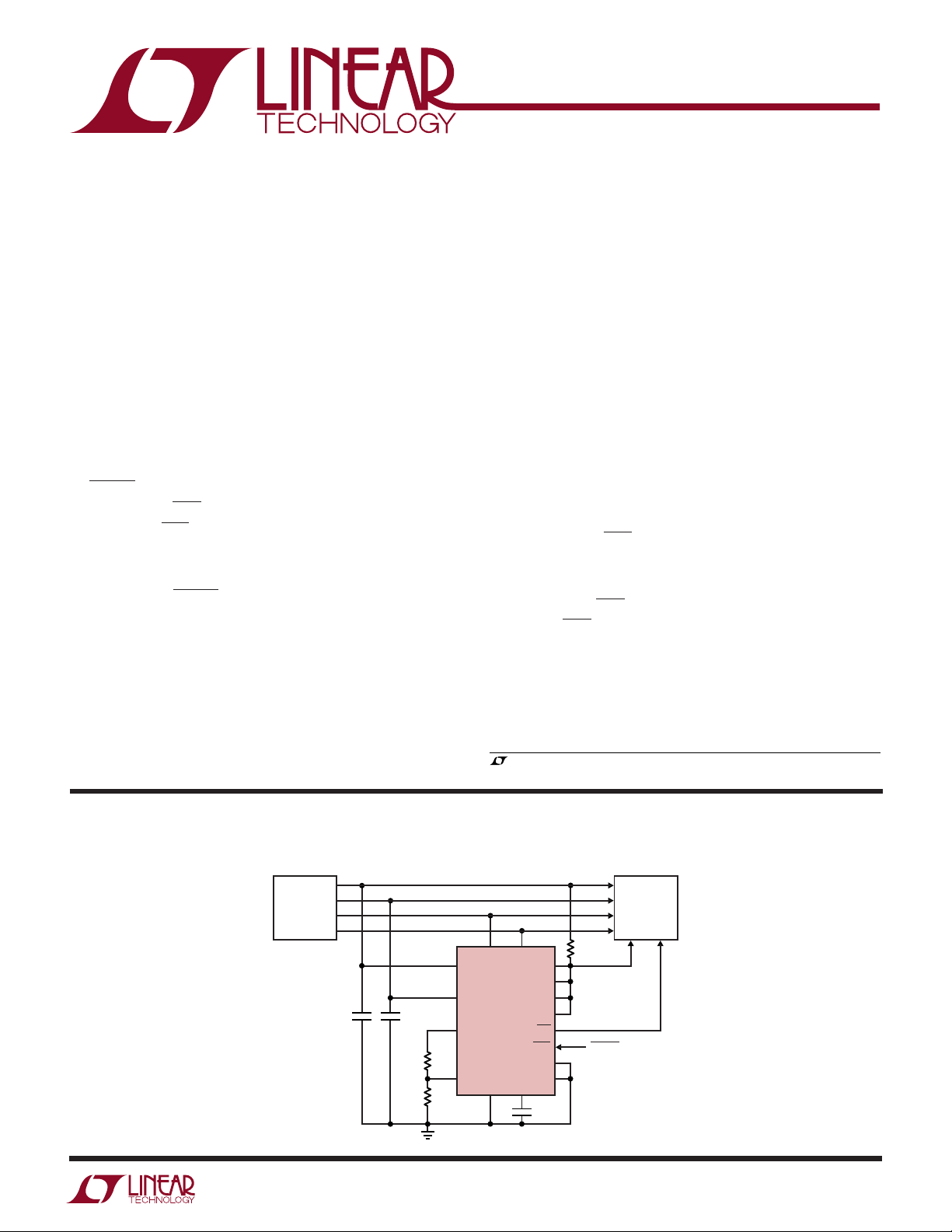
TYPICAL APPLICATIO
Quad Supply Monitor with Adjustable Tolerance (5V, 3.3V, 2.5V, 1.8V)
CONVERTER
DC/DC
U
0.1µF
5V
3.3V
2.5V
1.8V
C1
C2
0.1µF
59k
1%
40.2k
1%
SYSTEM
LOGIC
133
LTC2902-2
GND
10
V4V3
CRT
COMP1
COMP2
COMP3
COMP4
5
4
V1
14
V2
12
V
REF
R1
11
V
R2
PG
RST
RDIS
C
47nF
T0
T1
RT
R3
10k
2
16
1
15
6
8
7
TOLERANCE = 5%
9
2902 TA01
POWER
GOOD
MARGIN
t
RST
= 216ms
2902f
1
Page 2
LTC2902
PACKAGE/ORDER I FOR ATIO
UU
W
GN PACKAGE
16-LEAD PLASTIC SSOP
1
2
3
4
5
6
7
8
TOP VIEW
16
15
14
13
12
11
10
9
COMP3
COMP1
V3
V1
CRT
RST
T0
RDIS
COMP2
COMP4
V2
V4
V
REF
V
PG
GND
T1
WWWU
ABSOLUTE AXI U RATI GS
(Notes 1, 2, 3)
V1, V2, V3, V4, VPG..................................... –0.3V to 7V
RST (LTC2902-1)........................................ –0.3V to 7V
RST (LTC2902-2).......................... –0.3V to (V2 + 0.3V)
COMPX, RDIS ............................................. – 0.3V to 7V
T0, T1 .......................................... –0.3V to (VCC + 0.3V)
CRT ............................................. –0.3V to (VCC + 0.3V)
V
............................................. – 0.3V to (VCC + 0.3V)
REF
Reference Load Current (I
V4 Input Current (–ADJ Mode) ............................ –1mA
Operating Temperature Range
LTC2902-1C/LTC2902-2C ....................... 0°C to 70°C
LTC2902-1I/LTC2902-2I .................... –40°C to 85°C
Storage Temperature Range .................. – 65°C to 150°C
Lead Temperature (Soldering, 10 sec)................... 300°C
) ............................ ±1mA
VREF
ORDER PART
NUMBER
LTC2902-1CGN
LTC2902-2CGN
LTC2902-1IGN
LTC2902-2IGN
GN16 PART MARKING
29021
29022
T
= 125°C, θJA = 130°C/W
JMAX
Consult LTC Marketing for parts specified with wider operating temperature ranges.
29021I
29022I
ELECTRICAL CHARACTERISTICS
temperature range, otherwise specifications are at TA = 25°C. VCC = 5V, unless otherwise noted. (Note 3)
SYMBOL PARAMETER CONDITIONS MIN TYP MAX UNITS
V
RT50
V
RT33
V
RT30
V
RT25
V
RT18
V
RT15
V
RTA
2
5V, 5% Reset Threshold V1 Input Threshold ● 4.600 4.675 4.750 V
5V, 7.5% Reset Threshold
5V, 10% Reset Threshold
5V, 12.5% Reset Threshold
3.3V, 5% Reset Threshold V1, V2 Input Threshold ● 3.036 3.086 3.135 V
3.3V, 7.5% Reset Threshold
3.3V, 10% Reset Threshold
3.3V, 12.5% Reset Threshold
3V, 5% Reset Threshold V2 Input Threshold ● 2.760 2.805 2.850 V
3V, 7.5% Reset Threshold
3V, 10% Reset Threshold
3V, 12.5% Reset Threshold
2.5V, 5% Reset Threshold V2, V3 Input Threshold ● 2.300 2.338 2.375 V
2.5V, 7.5% Reset Threshold
2.5V, 10% Reset Threshold
2.5V, 12.5% Reset Threshold
1.8V, 5% Reset Threshold V3, V4 Input Threshold ● 1.656 1.683 1.710 V
1.8V, 7.5% Reset Threshold
1.8V, 10% Reset Threshold
1.8V, 12.5% Reset Threshold
1.5V, 5% Reset Threshold V3, V4 Input Threshold ● 1.380 1.403 1.425 V
1.5V, 7.5% Reset Threshold
1.5V, 10% Reset Threshold
1.5V, 12.5% Reset Threshold
ADJ, 5% Reset Threshold V3, V4 Input Threshold ● 0.492 0.500 0.508 V
ADJ, 7.5% Reset Threshold
ADJ, 10% Reset Threshold
ADJ, 12.5% Reset Threshold
The ● denotes the specifications which apply over the full operating
● 4.475 4.550 4.625 V
● 4.350 4.425 4.500 V
● 4.225 4.300 4.375 V
● 2.954 3.003 3.053 V
● 2.871 2.921 2.970 V
● 2.789 2.838 2.888 V
● 2.685 2.730 2.775 V
● 2.610 2.655 2.700 V
● 2.535 2.580 2.625 V
● 2.238 2.275 2.313 V
● 2.175 2.213 2.250 V
● 2.113 2.150 2.188 V
● 1.611 1.638 1.665 V
● 1.566 1.593 1.620 V
● 1.521 1.548 1.575 V
● 1.343 1.365 1.388 V
● 1.305 1.328 1.350 V
● 1.268 1.290 1.313 V
● 0.479 0.487 0.494 V
● 0.466 0.473 0.481 V
● 0.453 0.460 0.467 V
2902f
Page 3
LTC2902
ELECTRICAL CHARACTERISTICS
The ● denotes the specifications which apply over the full operating
temperature range, otherwise specifications are at TA = 25°C. VCC = 5V, unless otherwise noted. (Note 3)
SYMBOL PARAMETER CONDITIONS MIN TYP MAX UNITS
V
RTAN
V
CC
V
CCMINP
V
CCMINC
V
REF
V
PG
I
VPG
I
V1
I
V2
I
V3
I
V4
I
CRT(UP)
I
CRT(DN)
t
RST
t
UV
V
OL
V
OH
V
OH
Digital Inputs T0, T1, RDIS
V
IL
V
IH
I
INTOL
V
IL
V
IH
I
RDIS
Note 1: Absolute Maximum Ratings are those values beyond which the life of
a device may be impaired.
Note 2: All voltage values are with respect to GND.
Note 3: The greater of V1, V2 is the internal supply voltage (V
Note 4: Under static no-fault conditions, V1 will necessarily supply quiescent
current. If at any time V2 is larger than V1, V2 must be capable of supplying
the quiescent current, programming (transient) current and reference load
current.
–ADJ Reset Threshold V4 Input Threshold ● –18 0 18 mV
Minimum Internal Operating Voltage RST, COMPX in Correct Logic State; ● 1V
VCC Rising Prior to Program
Minimum Required for Programming VCC Rising ● 2.42 V
Minimum Required for Comparators VCC Falling ● 2.32 V
Reference Voltage VCC ≥ 2.3V, I
= ±1mA, C
VREF
≤ 1000pF
REF
T0 Low, T1 Low ● 1.192 1.210 1.228 V
T0 Low, T1 High
● 1.160 1.178 1.195 V
T0 High, T1 Low ● 1.128 1.146 1.163 V
T0 High, T1 High
Programming Voltage Range VCC ≥ V
VPG Input Current VPG = V
CCMINP
REF
V1 Input Current V1 = 5V, I
= 12µA, (Note 4) ● 43 75 µA
VREF
● 1.096 1.113 1.130 V
● 0V
● ±20 nA
REF
V2 Input Current V2 = 3.3V ● 0.8 2 µA
V3 Input Current V3 = 2.5V ● 0.52 1.2 µA
V3 = 0.55V (ADJ Mode) –15 15 nA
V4 Input Current V4 = 1.8V ● 0.34 0.8 µA
V4 = 0.55V (ADJ Mode)
● –15 15 nA
V4 = –0.05V (–ADJ Mode) ● –15 15 nA
CRT Pull-Up Current V
CRT Pull-Down Current V
= 0V ● –1.4 –2 –2.6 µA
CRT
= 1.3V ● 10 20 30 µA
CRT
Reset Time-Out Period CRT = 1500pF ● 579 ms
VX Undervoltage Detect to RST or COMPX VX Less Than Reset Threshold V
RTX
150 µs
by More Than 1%
Output Voltage Low RST, COMPX I
= 2.5mA; V1 = 3V, V2 = 3V; ● 0.15 0.4 V
SINK
V3, V4 = 0V; VPG = 0V
I
= 100µA; V2 = 1V; V1, V3, V4 = 0V ● 0.05 0.3 V
SINK
I
= 100µA; V1 = 1V; V2, V3, V4 = 0V ● 0.05 0.3 V
SINK
Output Voltage High RST, COMPX (Note 5) I
Output Voltage High RST (LTC2902-2) I
= 1µA ● V2 – 1 V
SOURCE
= 200µA ● 0.8 • V2 V
SOURCE
(Note 6)
T0, T1 Low Level Input Voltage VCC = 3.3V to 5.5V ● 0.3V
T0, T1 High Level Input Voltage VCC = 3.3V to 5.5V ● 0.7V
T0, T1 Input Current T0 = 0V, T1 = V
CC
● ±0.1 ±1 µA
CC
CC
RDIS Input Threshold Low VCC = 3.3V to 5.5V ● 0.4 V
RDIS Input Threshold High VCC = 3.3V to 5.5V ● 1.6 V
RDIS Pull-Up Current V
= 0V –10 µA
RDIS
Note 5: The output pins RST and COMPX have internal pull-ups to V2 of
typically 6µA. However, external pull-up resistors may be used when faster
CC
rise times are required or for V
).
Note 6: The push-pull RST output pin on the LTC2902-2 is
to V2.
voltages greater than V2.
OH
actively
pulled up
2902f
V
V
V
3
Page 4
LTC2902
TEST CIRCUITS
V1
V2
V3
V4
LTC2902-1
2902 F01
RST
OR COMPX
I
SOURCE
1µA
V1
V2
V3
V4
LTC2902-1
2902 F02
RST
OR COMPX
I
SINK
2.5mA,
100µA
V1
V2
V3
V4
LTC2902-2
2902 F03
RST
I
SOURCE
200µA
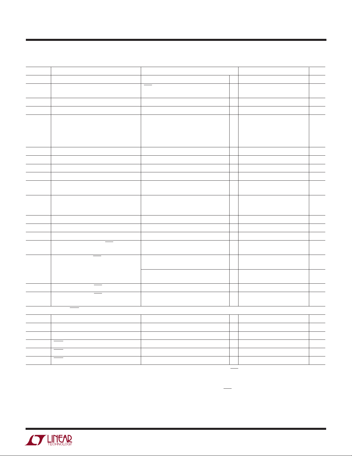
Figure 1. RST, COMPX VOH Test Figure 2. RST, COMPX VOL Test Figure 3. Active Pull-Up RST VOH Test
UWW
TI I G DIAGRA
VX Monitor Timing
V
RTX
t
t
UV
RST
1.5V
2902 TD
RST
COMPX
V
X
UW
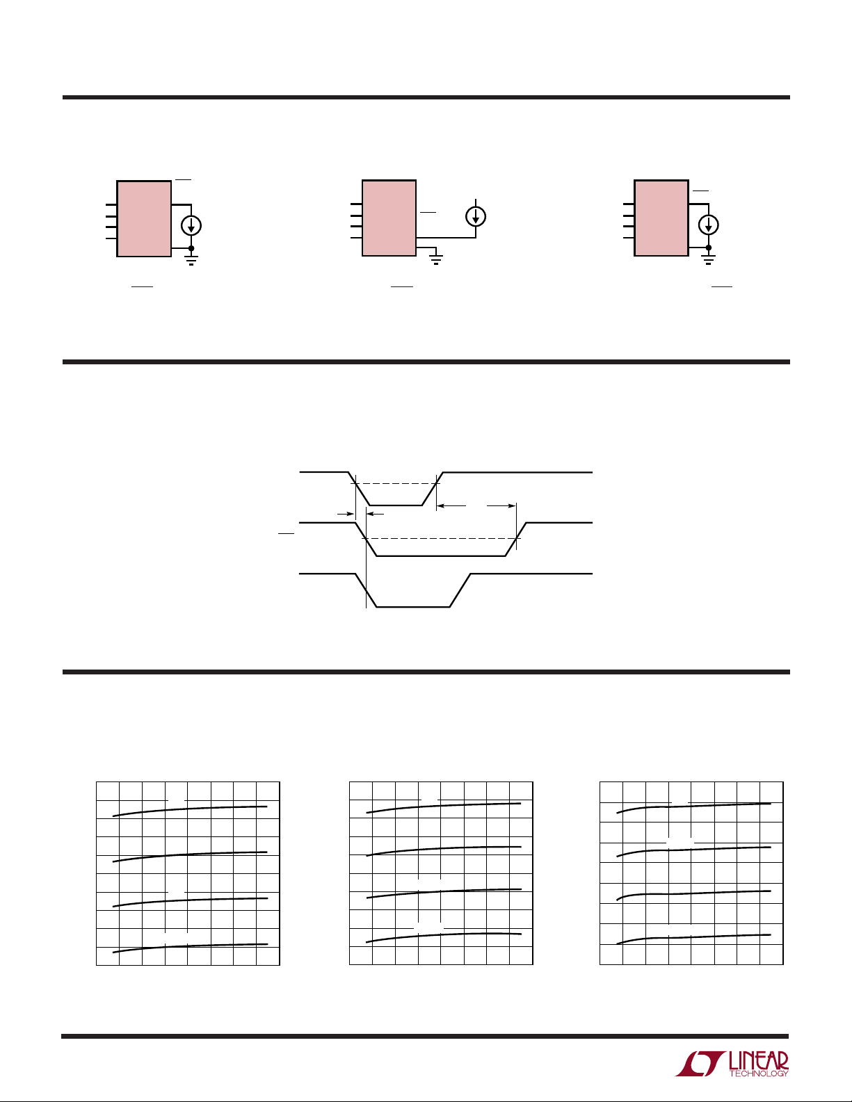
TYPICAL PERFOR A CE CHARACTERISTICS
5V Threshold Voltage
vs Temperature
4.75
4.70
(V)
4.65
RT50
4.60
4.55
4.50
4.45
4.40
4.35
THRESHOLD VOLTAGE, V
4.30
4.25
–60
–20
–40 0
TEMPERATURE (°C)
5%
7.5%
10%
12.5%
20
40
80
60
100
2902 G01
3.3V Threshold Voltage
vs Temperature
3.135
3.100
3.065
(V)
RT33
3.030
2.995
2.960
2.925
2.890
2.855
THRESHOLD VOLTAGE, V
2.820
2.785
–60
–20
–40 0
TEMPERATURE (°C)
5%
7.5%
10%
12.5%
20
60
40
4
80
2902 G02
100
3V Threshold Voltage
vs Temperature
2.850
2.815
(V)
2.780
RT30
2.745
2.710
2.675
2.640
2.605
THRESHOLD VOLTAGE, V
2.570
2.535
–60
–20
–40 0
TEMPERATURE (°C)
5%
7.5%
10%
12.5%
20
40
80
60
100
2902 G03
2902f
Page 5
UW
TYPICAL PERFOR A CE CHARACTERISTICS
LTC2902
2.5V Threshold Voltage
vs Temperature
2.375
2.350
2.325
(V)
2.300
RT25
2.275
2.250
2.225
2.200
2.175
2.150
THRESHOLD VOLTAGE, V
2.125
2.100
–60
–20
–40 0
TEMPERATURE (°C)
ADJ Threshold Voltage
vs Temperature
0.508
0.503
0.498
(V)
0.493
RTA
0.488
0.483
0.478
0.473
0.468
0.463
THRESHOLD VOLTAGE, V
0.458
0.453
–60
–20
–40 0
TEMPERATURE (°C)
5%
7.5%
10%
12.5%
5%
7.5%
10%
12.5%
1.8V Threshold Voltage
vs Temperature
1.710
1.685
(V)
1.660
RT18
1.635
1.610
1.585
1.560
THRESHOLD VOLTAGE, V
1.535
100
1.510
–60
–40 0
20
40
80
60
2902 G04
5%
7.5%
10%
12.5%
–20
20
TEMPERATURE (°C)
40
100
2902 G05
80
60
1.5V Threshold Voltage
vs Temperature
1.425
1.405
(V)
1.385
RT15
1.365
1.345
1.325
1.305
THRESHOLD VOLTAGE, V
1.285
1.265
–60
–20
–40 0
TEMPERATURE (°C)
5%
7.5%
10%
12.5%
20
40
80
60
100
2902 G06
–ADJ Threshold Voltage
vs Temperature
0.018
0.012
(V)
RTAN
0.006
0
–0.006
–0.012
THRESHOLD VOLTAGE, V
100
–0.018
–60
–40 0
–20
20
TEMPERATURE (°C)
40
100
2902 G08
80
60
20
40
80
60
2902 G07
1.228
1.216
1.204
1.192
1.180
1.168
(V)
REF
1.156
V
1.144
1.132
1.112
1.108
1.096
V
vs Temperature
REF
–60
–20
–40 0
5%
7.5%
10%
12.5%
20
TEMPERATURE (°C)
40
80
60
100
2902 G09
IV1 vs Temperature
100
V1 = 5V
90
V2 = 3.3V
V3 = 2.5V
80
V4 = 1.8V
70
60
50
(µA)
V1
I
40
30
20
10
0
–60
–40 0
–20
20
TEMPERATURE (°C)
40
IV2 vs Temperature
1.5
V1 = 5V
1.4
V2 = 3.3V
V3 = 2.5V
1.3
V4 = 1.8V
1.2
1.1
1.0
(µA)
V2
I
0.9
0.8
0.7
0.6
80
60
100
2902 G10
0.5
–60
–40 0
–20
TEMPERATURE (°C)
80
20
60
40
100
2902 G11
IV3 vs Temperature
1.1
V1 = 5V
1.0
V2 = 3.3V
V3 = 2.5V
0.9
V4 = 1.8V
0.8
0.7
0.6
(µA)
V3
I
0.5
0.4
0.3
0.2
0.1
–60
–40 0
–20
20
TEMPERATURE (°C)
40
80
60
100
2902 G12
2902f
5
Page 6

LTC2902
UW
TYPICAL PERFOR A CE CHARACTERISTICS
IV4 vs Temperature
1.0
V1 = 5V
0.9
V2 = 3.3V
V3 = 2.5V
0.8
V4 = 1.8V
0.7
0.6
0.5
(µA)
V4
I
0.4
0.3
0.2
0.1
0
–60
–40 0
–20
20
TEMPERATURE (°C)
40
RST Output Voltage
vs V1, VPG = 0V
5
V1 = V2 = V3 = V4
10k PULL-UP FROM RST TO V1
T
= 25°C
4
A
3
2
RST OUTPUT VOLTAGE (V)
1
0
0 0.5 1.0 1.5 2.0 2.5 3.0 3.5 4.0 4.5 5.0
V1 (V)
Typical Transient Duration
vs Comparator Overdrive (V1, V2)
450
400
350
300
250
200
150
100
TYPICAL TRANSIENT DURATION (µs)
50
0
80
60
100
2902 G13
0.1
RESET COMPARATOR OVERDRIVE VOLTAGE (% OF V
RESET OCCURS
ABOVE CURVE
1 10 100
TA = 25°C
2902 G14
RTX
Reset Time-Out Period
vs Temperature
8.9
CRT = 1500pF
(SILVER MICA)
8.4
(ms)
7.9
RST
7.4
6.9
6.4
5.9
RESET TIME-OUT PERIOD, t
5.4
2902 G15
4.9
–60
–40 0
–20
TEMPERATURE (°C)
20
40
80
60
100
2902 G16
Typical Transient Duration
vs Comparator Overdrive (V3, V4)
220
200
180
160
140
120
100
80
60
40
TYPICAL TRANSIENT DURATION (µs)
20
0
0.1
RESET COMPARATOR OVERDRIVE VOLTAGE (% OF V
)
RESET OCCURS
ABOVE CURVE
1 10 100
Reset Time-Out Period
vs Capacitance
10
TA = 25°C
1
(sec)
RST
100m
10m
1m
RESET TIME-OUT PERIOD, t
100µ
10p 100p 10n 1µ
1n
CRT (FARAD)
TA = 25°C
2902 G25
100n
2902 G17
RTX
)
RST, COMPX I
vs Supply Voltage
10
TA = 25°C
9
8
7
6
(mA)
5
SINK
I
4
3
2
1
0
0
6
1
SINK
34
2
V1 OR V2 (V)
VOL = 0.4V
VOL = 0.2V
5
2902 G18
RST High Level Output Voltage
RST, COMPX Voltage Output Low
vs Output Sink Current
3.0
V2 = 3V
V1 = 5V
2.5
2.0
(V)
1.5
OL
V
1.0
0.5
6
0
0
10 30
85°C
20
40
I
(mA)
SINK
25°C
–40°C
70
50 90
60
80
2902 G19
vs Output Source Current
(LTC2902-2)
3.5
3.0
2.5
2.0
(V)
OH
V
1.5
1.0
0.5
0
0 0.5 2
85°C
I
SOURCE
1.51
(mA)
V1 = 5V
V2 = 3V
V3 = 2.5V
V4 = 1V
–40°C
25°C
2.5
2902 G20
2902f
Page 7

UW
TYPICAL PERFOR A CE CHARACTERISTICS
LTC2902
COMPX Pull-Up Current
vs V2 (COMPX Held at 0V)
20
TA = 25°C
18
16
14
12
10
8
6
PULL-UP CURRENT (µA)
4
2
0
1
1.5 2.5
2
V2 (V)
RST Pull-Up Current vs V2
(LTC2902-1)
20
TA = 25°C
18
16
14
12
10
8
V
RT25
2.5
V
RT30
V
RT33
3
3.5 4
V2 (V)
6
PULL-UP CURRENT (µA)
4
2
0
2
COMPX Propagation Delay vs
Input Overdrive Above Threshold
250
200
150
100
V1, V2
50
COMPX PROPAGATION DELAY (µs)
3.5
4
5
2902 G21
3
4.5
0
10 100
INPUT OVERDRIVE ABOVE THRESHOLD (mV)
V3, V4
TA = 25°C
1000
2902 G22
RST Pull-Up Current vs V2
(LTC2902-2)
6
TA = 25°C
5
4
3
V
RT25
2.5
V
RT30
RT33
3
3.5 4
V2 (V)
4.5
5
2902 G24
4.5
2902 G23
2
PULL-UP CURRENT (mA)
V
1
0
5
2
U
UU
PI FU CTIO S
COMP3 (Pin 1): Comparator Output 3. Nondelayed, active
high logic output with weak pull-up to V2. Pulls high when
V3 is above reset threshold. May be pulled greater than V2
using external pull-up.
COMP1 (Pin 2): Comparator Output 1. Nondelayed, active
high logic output with weak pull-up to V2. Pulls high when
V1 is above reset threshold. May be pulled greater than V2
using external pull-up.
V3 (Pin 3): Voltage Input 3. Select from 2.5V, 1.8V, 1.5V
or ADJ. See Table 1 for details.
V1 (Pin 4): Voltage Input 1. Select from 5V or 3.3V. See
Table 1 for details. The greater of (V1, V2) is also VCC for
the chip. Bypass this pin to ground with a 0.1µF (or
greater) capacitor.
CRT (Pin 5): Reset Delay Time Programming Pin. Attach
an external capacitor (CRT) to GND to set a reset delay time
of 4.6ms/nF. Leaving the pin open generates a minimum
delay of approximately 50µs. A 47nF capacitor will gener-
ate a 216ms reset delay time.
2902f
7
Page 8

LTC2902
U
UU
PI FU CTIO S
RST (Pin 6): Reset Logic Output. Active low with weak
pull-up to V2 (LTC2902-1) or active pull-up to V2
(LTC2902-2). Pulls low when any voltage input is below
the reset threshold and held low for programmed delay
time after all voltage inputs are above threshold. May be
pulled above V2 using an external pull-up (LTC2902-1
only).
T0 (Pin 7): Digital Input for Supply Tolerance Selection
(5%, 7.5%, 10% or 12.5%). Used in conjunction with T1
(Pin 9). See Applications Information for tolerance selection chart (Table 4).
RDIS (Pin 8): Digital Input for RST Disable. A low input on
this pin forces the RST output to V2 (or pull-up voltage).
Useful for determining supply margins without issuing
reset command to processor. A weak internal pull-up
allows pin to be left floating for normal monitor operation.
T1 (Pin 9): Digital Input for Supply Tolerance Selection
(5%, 7.5%, 10% or 12.5%). Used in conjunction with T0
(Pin 7). See Applications Information for tolerance selection chart (Table 4).
GND (Pin 10): Ground.
VPG (Pin 11):
Input. Connect to an external 1% resistive divider between V
preset and/or ±adjustable voltage thresholds (see Table␣ 1).
Do not add capacitance on the VPG pin.
REF
Voltage Threshold Combination Select
and GND to select 1 of 16 combinations of
V
(Pin 12): Buffered Reference Voltage. A 1.210V
REF
nominal reference used for programming voltage (VPG)
and for the offset of negative adjustable applications. The
buffered reference can source and sink up to 1mA. The
reference can drive a bypass capacitor of up to 1000pF
without oscillation.
V4 (Pin 13): Voltage Input 4. Select from 1.8V, 1.5V, ADJ
or –ADJ. See Table 1 for details.
V2 (Pin 14): Voltage Input 2. Select from 3.3V, 3V or 2.5V.
See Table 1 for details. The greater of (V1, V2) is also V
for chip. Bypass this pin to ground with a 0.1µF (or greater)
capacitor. All logic outputs (COMP1, COMP2, COMP3,
COMP4) are weakly pulled up to V2. RST is weakly pulled
up to V2 in the LTC2902-1 and RST is actively pulled up to
V2 in the LTC2902-2.
COMP4 (Pin 15): Comparator Output 4. Nondelayed,
active high logic output with weak pull-up to V2. Pulls high
when V4 is above reset threshold. May be pulled greater
than V2 using external pull-up.
COMP2 (Pin 16): Comparator Output 2. Nondelayed,
active high logic output with weak pull-up to V2. Pulls high
when V2 is above reset threshold. May be pulled greater
than V2 using external pull-up.
CC
8
2902f
Page 9

BLOCK DIAGRA
W
V1
POWER
DETECT
LTC2902
V2
V
CC
6µA
V1
V2
14
V3
V4
13
GND
10
V
11
V
REF
12
–
V2
COMP1
2
+
V2
–
4
+
RESISTIVE
DIVIDER
3
MATRIX
–
6µA
COMP2
16
V2
+
6µA
–
PG
A/D
BUFFER
+
BANDGAP
REFERENCE
COMP3
1
V2
6µA
COMP4
15
BUFFER
GAIN
ADJUST
T0
7
ADJUSTABLE
RESET PULSE
GENERATOR
22µA
T1
9
CRT
5
C
RT
V
CC
2µA
10µA
V
CC
RDIS
8
V2
LTC2902-1
6µA
LTC2902-2
V2
RST
6
RST
6
2902 DB-1
2902f
9
Page 10

LTC2902
WUUU
APPLICATIO S I FOR ATIO
Power-Up
On power-up, the larger of V1 or V2 will power the drive
circuits for the RST and the COMPX pins. This ensures
that the RST and COMPX outputs will be low as soon as
V1 or V2 reaches 1V. The RST and COMPX outputs will
remain low until the part is programmed. After programming, if any one of the VX inputs is below its programmed
threshold, RST will be a logic low. Once all the VX inputs
rise above their thresholds, an internal timer is started
and RST is released after the programmed delay time. If
VCC < (V3 – 1) and VCC < 2.4V, the V3 input impedance
will be low (1kΩ typ).
Monitor Programming
The LTC2902 input voltage combination is selected by
placing the recommended resistor divider from V
GND and connecting the tap point to VPG, as shown in
Figure 4. Table 1 offers recommended 1% resistor values
for the various modes. The last column in Table 1 specifies optimum VPG/V
pro
gramming with a ratiometric DAC.
ratios (±0.01) to be used when
REF
During power-up, once V1 or V2 reaches 2.4V (max), the
monitor enters a programming period of approximately
150µs during which the voltage on the VPG pin is sampled
and the monitor is configured to the desired input combination. Do not add capacitance to the VPG pin. Immediately
after programming, the comparators are enabled and
supply monitoring will begin.
Supply Monitoring
The LTC2902 is a low power, high accuracy programmable quad supply monitoring circuit with four nondelayed
monitor outputs, a common reset output and selectable
supply thresholds. Reset timing is adjustable using an
external capacitor. Single pin programming selects 1 of 16
input voltage monitor combinations. Two digital inputs
select one of four supply tolerances (5%, 7.5%, 10% or
12.5%). All four voltage inputs must be above predetermined thresholds for the reset not to be invoked. The
LTC2902 will assert the reset and comparator outputs
during power-up, power-down and brownout conditions
on any one of the voltage inputs.
REF
to
LTC2902
V
REF
V
PG
GND
Figure 4. Monitor Programming
Table 1. Voltage Threshold Programming
MODE V1 (V) V2 (V) V3 (V) V4 (V) R1 (kΩ) R2 (kΩ)V
0 5.0 3.3 ADJ ADJ Open Short 0.000
1 5.0 3.3 ADJ –ADJ 93.1 9.53 0.094
2 3.3 2.5 ADJ ADJ 86.6 16.2 0.156
3 3.3 2.5 ADJ –ADJ 78.7 22.1 0.219
4 3.3 2.5 1.5 ADJ 71.5 28.0 0.281
5 5.0 3.3 2.5 ADJ 66.5 34.8 0.344
6 5.0 3.3 2.5 1.8 59.0 40.2 0.406
7 5.0 3.3 2.5 1.5 53.6 47.5 0.469
8 5.0 3.0 2.5 ADJ 47.5 53.6 0.531
9 5.0 3.0 ADJ ADJ 40.2 59.0 0.594
10 3.3 2.5 1.8 1.5 34.8 66.5 0.656
11 3.3 2.5 1.8 ADJ 28.0 71.5 0.719
12 3.3 2.5 1.8 –ADJ 22.1 78.7 0.781
13 5.0 3.3 1.8 –ADJ 16.2 86.6 0.844
14 5.0 3.3 1.8 ADJ 9.53 93.1 0.906
15 5.0 3.0 1.8 ADJ Short Open 1.000
R1
1%
12
11
10
R2
1%
2902 F04
V
PG
REF
The inverting inputs on the V3 and/or V4 comparators are
set to 0.5V when the positive adjustable modes are selected
and with T0 and T1 low (5% tolerance) (Figure 5). The tap
point on an external resistive divider, connected between
the positive voltage being sensed and ground, is connected
to the high impedance noninverting inputs (V3, V4). The
trip voltage is calculated from:
R
3
VV
=+
TRIP
05 1
.
R
4
Once the resistor divider is set in the 5% tolerance mode,
there is no need to change the divider for the other
tolerance modes (7.5%, 10%, 12.5%) because the internal reference is scaled accordingly, moving the trip point
in –2.5% increments.
10
2902f
Page 11

WUUU
APPLICATIO S I FOR ATIO
LTC2902
V
TRIP
R3
V3 OR V4
Figure 5. Setting the Positive Adjustable Trip Point
Figure 6. Setting the Negative Adjustable Trip Point
1%
R4
1%
12
V
R4
1%
R3
1%
V
TRIP
REF
V4
13
LTC2902
+
–
0.5V
+
–
5% TOLERANCE MODE
LTC2902
–
+
2902 F05
2902 F06
In the negative adjustable mode, the noninverting input on
the V4 comparator is connected to ground (Figure 6). The
tap point on an external resistive divider, connected between the negative voltage being sensed and the V
REF
pin,
is connected to the high impedance inverting input (V4).
V
provides the necessary level shift required to operate
REF
at ground. The trip voltage is calculated from:
R
3
VV
=
TRIP REF REF
VV
=–;.
R
4
1 210
Table 2. Suggested 1% Resistor Values for the ADJ Inputs
V
(V) V
SUPPLY
12 11.25 2150 100
10 9.4 1780 100
8 7.5 1400 100
7.5 7 1300 100
6 5.6 1020 100
5 4.725 845 100
3.3 3.055 511 100
3 2.82 464 100
2.5 2.325 365 100
1.8 1.685 237 100
1.5 1.410 182 100
1.2 1.120 124 100
1 0.933 86.6 100
0.9 0.840 68.1 100
Table 3. Suggested 1% Resistor Values for the –ADJ Input
V
(V) V
SUPPLY
–2 –1.87 187 121
–5 –4.64 464 121
–5.2 –4.87 487 121
–10 –9.31 931 121
–12 –11.30 1130 121
(V) R3 (kΩ) R4 (kΩ)
TRIP
(V) R3 (kΩ) R4 (kΩ)
TRIP
Although all four supply monitor comparators have built-in
glitch immunity, bypass capacitors on V1 and V2 are
recommended because the greater of V1 or V2 is also the
VCC for the chip. Filter capacitors on the V3 and V4 inputs
are allowed.
T0,T1 Low (5% Tolerance Mode)
Once the resistor divider is set in the 5% tolerance mode,
there is no need to change the divider for the other
tolerance modes (7.5%, 10%, 12.5%) because V
REF
is
scaled accordingly, moving the trip point in –2.5%
increments.
In a negative adjustable application, the minimum value
for R4 is limited by the sourcing capability of V
With no other load on V
, R4 (minimum) is:
REF
( ±1mA).
REF
1.21V ÷ 1mA = 1.21kΩ
Tables 2 and 3 offer suggested 1% resistor values for
various adjustable applications.
Power-Down
On power-down, once any of the VX inputs drop below
their threshold, RST and COMPX are held at a logic low.
A logic low of 0.4V is guaranteed until both V1 and V2
drop below 1V. If the bandgap reference becomes invalid
(VCC < 2V typ), the part will reprogram once VCC rises
above 2.4V (max).
Monitor Output Rise and Fall Time Estimation
All of the outputs (RST, COMPX) have strong pull-down
capability. If the external load capacitance (C
LOAD
) for a
2902f
11
Page 12

LTC2902
WUUU
APPLICATIO S I FOR ATIO
particular output is known, output fall time (10% to 90%)
is estimated using:
t
≈ 2.2 • RPD • C
FALL
LOAD
where RPD is the on-resistance of the internal pull-down
transistor. The typical performance curve (VOL vs I
SINK
)
demonstrates that the pull-down current is somewhat
linear versus output voltage. Using the 25°C curve, RPD is
estimated to be approximately 40Ω. Assuming a 150pF
load capacitance, the fall time is about 13.2ns.
Although the outputs are considered to be “open-drain,”
they do have a weak pull-up capability (see COMPX or RST
Pull-Up Current vs V2 curve). Output rise time (10% to
90%) is estimated using:
t
≈ 2.2 • RPU • C
RISE
LOAD
where RPU is the on-resistance of the pull-up transistor.
The on-resistance as a function of the V2 voltage at room
temperature is estimated using:
5
610
R
PU
•
=Ω
V
21
–
with V2 = 3.3V, RPU is about 260k. Using 150pF for load
capacitance, the rise time is 86µs. If the output needs to
pull up faster and/or to a higher voltage, a smaller
external pull-up resistor may be used. Using a 10k pullup resistor, the rise time is reduced to 3.3µs for a 150pF
load capacitance.
The LTC2902-2 has an active pull-up to V2 on the RST
output. The typical performance curve (RST Pull-Up Current vs V2 curve) demonstrates that the pull-up current is
somewhat linear versus the V2 voltage and RPU is estimated to be approximately 625Ω. A 150pF load capacitance makes the rise time about 206ns.
Selecting the Reset Timing Capacitor
The reset time-out period is adjustable in order to accommodate a variety of microprocessor applications. The
reset time-out period, t
, is adjusted by connecting a
RST
capacitor, CRT, between the CRT pin and ground. The value
of this capacitor is determined by:
CRT = t
• 217 • 10
RST
–9
with CRT in Farads and t
in seconds. The CRT value per
RST
millisecond of delay can also be expressed as CRT/ms =
217 (pF/ms).
Leaving the CRT pin unconnected will generate a minimum reset time-out of approximately 50µs. Maximum
reset time-out is limited by the largest available low
leakage capacitor. The accuracy of the time-out period will
be affected by capacitor leakage (the nominal charging
current is 2µA) and capacitor tolerance. A low leakage
ceramic capacitor is recommended.
Tolerance Programming and the RESET Disable
Using the two digital inputs T0 and T1, the user can
program the global supply tolerance for the LTC2902 (5%,
7.5%, 10%, 12.5%). The larger tolerances provide more
headroom by lowering the trip thresholds.
Table 4. Tolerance Programming
T0 T1 TOLERANCE (%) V
Low Low 5 1.210
Low High 7.5 1.178
High Low 10 1.146
High High 12.5 1.113
REF
(V)
Under conventional operation, RST and COMPX will go
low when VX is below its threshold. At any time, the RDIS
pin can be pulled low, overriding the reset operation and
forcing the RST pin high. This feature is useful when
determining supply margins under processor control since
the reset command will not be invoked. The RDIS pin is
connected to a weak internal pull-up to VCC (10µA typ),
allowing the pin to be left floating if unused.
Ensuring RST Valid for VCC Down to 0V (LTC2902-2)
When VCC is below 1V the RST pull-down capability is
drastically reduced. The RST pin may float to undetermined voltages when connected to high impedance (such
as CMOS logic inputs). The addition of a pull-down resistor from RST to ground will provide a path for stray charge
and/or leakage currents. The resistor value should be
small enough to provide effective pull-down without excessively loading the pull-up circuitry. Too large a value
may not pull down well enough. A 100k resistor from RST
to ground is satisfactory for most applications.
2902f
12
Page 13

U
TYPICAL APPLICATIO S
LTC2902
Quad Supply Monitor, 5% Tolerance
5V, 3V, 1.8V, 12V (ADJ)
1
COMP3
2
COMP1
1.8V 3V
SYSTEM
RESET
C
RT
3
V3
4
5V
LTC2902
V1
5
CRT
6
RST
7
T0
8
RDIS
COMP2
COMP4
V
REF
V
GND
16
15
14
V2
13
V4
12
11
PG
10
9
T1
R3
2.15M
1%
R4
100k
1%
2902 TA02
5V, –5V Monitor with Unused V2, V3 Inputs Pulled
Above Trip Thresholds (5% Tolerance)
COMP2
COMP4
V
REF
V
GND
16
15
14
V2
13
V4
12
11
PG
10
9
T1
R1
16.2k
1%
R2
86.6k
1%
2902 TA03
5V
SYSTEM
RESET
C
RT
1
2
3
4
5
6
7
8
COMP3
COMP1
V3
LTC2902
V1
CRT
RST
T0
RDIS
R4
121k
1%
12V
V
TRIP
= 11.25V
R3
464k
1%
–5V
V
TRIP
= –4.64V
2902f
13
Page 14

LTC2902
TYPICAL APPLICATIO S
Quad Supply Monitor with LED Undervoltage Indicators,
U
12.5% Tolerance, Reset Disabled
5V, 3.3V, 2.5V, 1.5V
L1
LED
R
1k
LED
1
2
3
4
5
6
7
8
L3
COMP3
COMP1
V3
V1
CRT
RST
T0
RDIS
LTC2902
COMP2
COMP4
V
REF
V
GND
V2
V4
PG
T1
R
1k
2.5V
5V
C
RT
R
1k
16
15
14
13
12
11
10
9
L2
LED
2902 TA04
R
1k
3.3V
1.5V
R1
53.6k
1%
R2
47.5k
1%
L4
LED
14
2902f
Page 15

PACKAGE DESCRIPTIO
LTC2902
U
GN Package
16-Lead Plastic SSOP (Narrow .150 Inch)
(Reference LTC DWG # 05-08-1641)
.045 ±.005
.254 MIN
RECOMMENDED SOLDER PAD LAYOUT
.007 – .0098
(0.178 – 0.249)
.016 – .050
NOTE:
1. CONTROLLING DIMENSION: INCHES
2. DIMENSIONS ARE IN
3. DRAWING NOT TO SCALE
*DIMENSION DOES NOT INCLUDE MOLD FLASH. MOLD FLASH
SHALL NOT EXCEED 0.006" (0.152mm) PER SIDE
**DIMENSION DOES NOT INCLUDE INTERLEAD FLASH. INTERLEAD
FLASH SHALL NOT EXCEED 0.010" (0.254mm) PER SIDE
(0.406 – 1.270)
INCHES
(MILLIMETERS)
.150 – .165
.0250 TYP.0165 ±.0015
.015
(0.38 ± 0.10)
0° – 8° TYP
± .004
× 45°
.229 – .244
(5.817 – 6.198)
.053 – .068
(1.351 – 1.727)
.008 – .012
(0.203 – 0.305)
16
15
12
.189 – .196*
(4.801 – 4.978)
12 11 10
14
13
5
4
3
678
9
(0.102 – 0.249)
.0250
(0.635)
BSC
(0.229)
.150 – .157**
(3.810 – 3.988)
.004 – .0098
GN16 (SSOP) 0502
.009
REF
Information furnished by Linear Technology Corporation is believed to be accurate and reliable.
However, no responsibility is assumed for its use. Linear Technology Corporation makes no representation that the interconnection of its circuits as described herein will not infringe on existing patent rights.
2902f
15
Page 16

LTC2902
TYPICAL APPLICATIO
U
Quad Supply Monitor with Hysteresis
5% Tolerance (Supplies Rising)
12.5% Tolerance (After RST Goes High)
5V
3.3V
2.5V
1.8V
R1
59k
1%
R2
40.2k
1%
LTC2902-1
4
V1
14
V2
3
V3
13
V4
8
RDIS
12
V
REF
11
V
PG
10
GND
COMP1
COMP2
COMP3
COMP4
RST
CRT
T0
T1
2
16
1
15
6
7
9
5
2902 TA05
10k
C
RT
RELATED PARTS
PART NUMBER DESCRIPTION COMMENTS
LTC690 5V Supply Monitor, Watchdog Timer and Battery Backup 4.65V Threshold
LTC694-3.3 3.3V Supply Monitor, Watchdog Timer and Battery Backup 2.9V Threshold
LTC699 5V Supply Monitor and Watchdog Timer 4.65V Threshold
LTC1232 5V Supply Monitor, Watchdog Timer and Push-Button Reset 4.37V/4.62V Threshold
LTC1326 Micropower Precision Triple Supply Monitor for 5V, 3.3V and ADJ 4.725V, 3.118V, 1V Thresholds (±0.75%)
LTC1326-2.5 Micropower Precision Triple Supply Monitor for 2.5V, 3.3V and ADJ 2.363V, 3.118V, 1V Thresholds (±0.75%)
LTC1536 Precision Triple Supply Monitor for PCI Applications Meets PCI t
LTC1726-2.5 Micropower Triple Supply Monitor for 2.5V, 3.3V and ADJ Adjustable RESET and Watchdog Time-Outs
LTC1726-5 Micropower Triple Supply Monitor for 5V, 3.3V and ADJ Adjustable RESET and Watchdog Time-Outs
LTC1727-2.5/LTC1727-5 Micropower Triple Supply Monitor with Open-Drain Reset Individual Monitor Outputs in MSOP
LTC1728-1.8/LTC1728-3.3 Micropower Triple Supply Monitor with Open-Drain Reset 5-Lead SOT-23 Package
LTC1728-2.5/LTC1728-5 Micropower Triple Supply Monitor with Open-Drain Reset 5-Lead SOT-23 Package
LTC1985-1.8 Micropower Triple Supply Monitor with Push-Pull Reset Output 5-Lead SOT-23 Package
LTC2900 Programmable Quad Supply Monitor Adjustable RESET, 10-Lead MSOP Package
LTC2901 Programmable Quad Supply Monitor Adjustable RESET and Watchdog Timer,
16-Lead SSOP Package
Linear Technology Corporation
16
1630 McCarthy Blvd., Milpitas, CA 95035-7417
(408) 432-1900 ● FAX: (408) 434-0507
●
www.linear.com
Timing Specifications
FAIL
LT/TP 1002 2K • PRINTED IN USA
LINEAR TECHNOLOGY CORPORATION 2002
2902f
 Loading...