

Page 1
Electrical Specifications Subject to Change
LTC2656
Octal 16-/12-Bit Rail-to-Rail
DACs with 10ppm/°C
Max Reference
FEATURES
n
Precision 10ppm/°C Max Reference
n
Maximum INL Error: ±4LSB at 16 Bits
n
Guaranteed Monotonic over Temperature
n
Selectable Internal or External Reference
n
2.7V to 5.5V Supply Range (LTC2656-L)
n
Integrated Reference Buffers
n
Ultralow Crosstalk Between DACs(<1nV•s)
n
Power-On-Reset to Zero-Scale/Mid-scale
n
Asynchronous LDAC Update Pin
n
Tiny 20-Lead 4mm × 5mm QFN and 20-Lead
Thermally Enhanced TSSOP Packages
APPLICATIONS
n
Mobile Communications
n
Process Control and Industrial Automation
n
Instrumentation
n
Automatic Test Equipment
n
Automotive
DESCRIPTION
The LTC®2656 is a family of octal 16-/12-bit rail-to-rail
DACs with a precision integrated reference. The DACs have
built-in high performance, rail-to-rail, output buffers and
are guaranteed monotonic.The LTC2656-L has a full-scale
output of 2.5V with the integrated 10ppm/°C reference and
operates from a single 2.7V to 5.5V supply. The LTC2656-H
has a full-scale output of 4.096V with the integrated reference and operates from a 4.5V to 5.5V supply. Each DAC can
also operate with an external reference, which sets the DAC
full-scale output to two times the external reference voltage.
These DACs communicate via a SPI/MICROWIRE™ compatible 4-wire serial interface which operates at clock rates
up to 50MHz. The LTC2656 incorporates a power-on reset
circuit that is controlled by the PORSEL pin. If PORSEL
is tied to GND the DACs reset to zero-scale. If PORSEL is
tied to V
L, LT, LTC and LTM are registered trademarks of Linear Technology Corporation.
All other trademarks are the property of their respective owners.
Protected by U.S. Patents, including 5396245, 6891433.
, the DACs reset to mid-scale.
CC
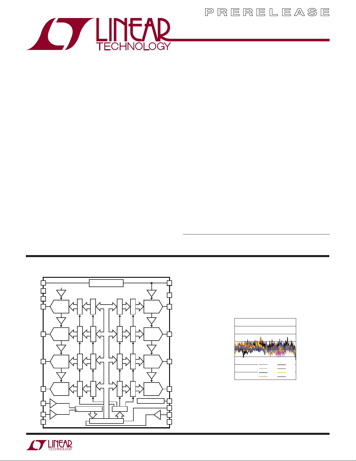
BLOCK DIAGRAM
REFCOMP REFIN/OUT
GND
REFLO
V
OUTA
V
OUTB
V
OUTC
V
OUTD
CS/LD
SCK
LDAC
REF
DAC A
REF
DAC B
REF
DAC C
REF
DAC D
INTERNAL REFERENCE
REGISTER
REGISTER
REGISTER
REGISTER
REGISTER
REGISTER
REGISTER
REGISTER
32-BIT SHIFT REGISTER
DECODECONTROL LOGIC
REGISTER
REGISTER
REGISTER
REGISTER
DAC H V
REGISTER
DAC G V
REGISTER
DAC F V
REGISTER
DAC E V
REGISTER
POWER-ON RESET
REF
REF
REF
REF
V
PORSEL
SDO
SDI
CLR
2656 BD
CC
OUTH
OUTG
OUTF
OUTE
4
3
2
1
0
INL (LSB)
–1
–2
–3
–4
128
INL vs Code
32768
16384
CODE
DACA
DACB
DACC
DACD
49152
DACE
DACF
DACG
DACH
2656 TA01
65535
2656p
1
Page 2
LTC2656
ABSOLUTE MAXIMUM RATINGS
(Notes 1, 2)
Supply Voltage (VCC) ................................... –0.3V to 6V
CS/LD, SCK, SDI, LDAC, CLR, REFLO .......... –0.3V to 6V
to V
V
OUTA
REFIN/OUT, REFCOMP ...... –0.3V to Min(V
PORSEL, SDO ................... –0.3V to Min(V
................. –0.3V to Min(VCC + 0.3V, 6V)
OUTH
+ 0.3V, 6V)
CC
+ 0.3V, 6V)
CC
Operating Temperature Range
LTC2656C ................................................ 0°C to 70°C
LTC2656I.............................................. –40°C to 85°C
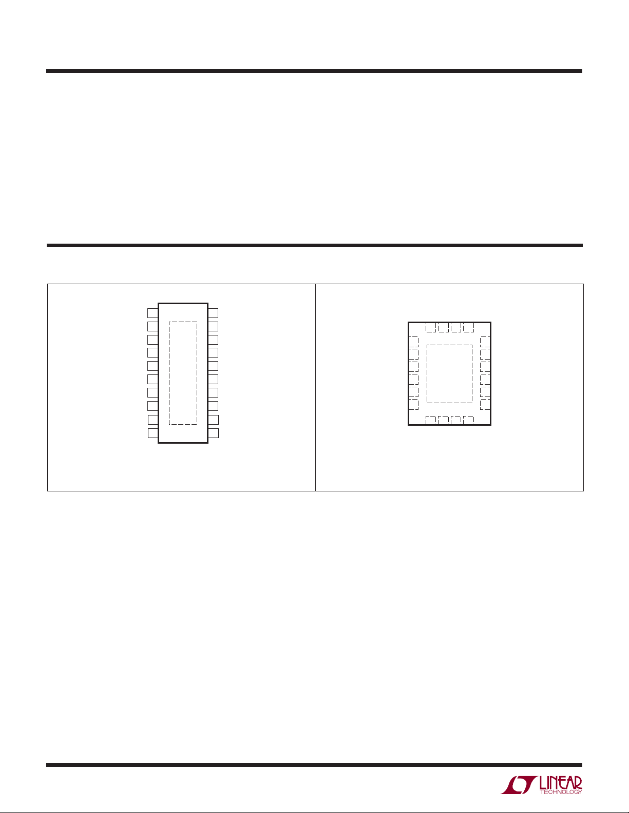
PIN CONFIGURATION
TOP VIEW
1
REFLO
2
V
OUTA
3
V
OUTB
REFCOMP
REFIN/OUT
EXPOSED PAD (PIN 21) IS GND, MUST BE SOLDERED TO PCB
4
5
V
OUTC
V
OUTD
LDAC
CS/LD
SCK
20-LEAD PLASTIC TSSOP
T
= 150°C, θJA = 38°C/W, θJC = 10°C/W
JMAX
6
7
8
9
10
21
FE PACKAGE
20
19
18
17
16
15
14
13
12
11
GND
V
CC
V
OUTH
V
OUTG
V
OUTF
V
OUTE
PORSEL
CLR
SDO
SDI
Maximum Junction Temperature........................... 150°C
Storage Temperature Range .......................–65 to 150°C
Lead Temperature (Soldering, 10 sec)
FE Package .......................................................300°C
TOP VIEW
OUTA
V
20 19 18 17
1
V
OUTB
REFCOMP
REFIN/OUT
EXPOSED PAD (PIN 21) IS GND, MUST BE SOLDERED TO PCB
2
V
3
OUTC
4
V
OUTD
5
6
LDAC
7 8
CS/LD
20-LEAD (4mm s 5mm) PLASTIC QFN
UFD PACKAGE
T
= 150°C, θJA = 43°C/W
JMAX
REFLO
21
9 10
SCK
GND
SDI
CC
V
SDO
16
15
14
13
12
11
V
OUTH
V
OUTG
V
OUTF
V
OUTE
PORSEL
CLR
2
2656p
Page 3
PRODUCT SELECTOR GUIDE
LTC2656 B C UFD -L 16 #TR PBF
LTC2656
LEAD FREE DESIGNATOR
PBF = Lead Free
TAPE AND REEL
TR = Tape and Reel
RESOLUTION
16 = 16-Bit
12 = 12-Bit
FULL-SCALE VOLTAGE, INTERNAL REFERENCE MODE
L = 2.5V
H = 4.096V
PACKAGE TYPE
UFD = 20-Lead (4mm × 5mm) Plastic QFN
FE = 20-Lead Thermally Enhanced TSSOP
TEMPERATURE GRADE
C = Commercial Temperature Range (0°C to 70°C)
I = Industrial Temperature Range (–40°C to 85°C)
ELECTRICAL GRADE (OPTIONAL)
B = ±4LSB Maximum INL (16-Bit)
PRODUCT PART NUMBER
Consult LTC Marketing for information on non-standard lead based fi nish parts.
For more information on lead free part marking, go to: http://www.linear.com/leadfree/
For more information on tape and reel specifi cations, go to: http://www.linear.com/tapeandreel/
2656p
3
Page 4
LTC2656
ORDER INFORMATION
LEAD FREE FINISH TAPE AND REEL
LTC2656BCFE-L16#PBF
LTC2656BIFE-L16#PBF
LTC2656BCUFD-L16#PBF
LTC2656BIUFD-L16#PBF
LTC2656BCFE-H16#PBF
LTC2656BIFE-H16#PBF
LTC2656BCUFD-H16#PBF
LTC2656BIUFD-H16#PBF
LTC2656CFE-L12#PBF
LTC2656IFE-L12#PBF
LTC2656CUFD-L12#PBF
LTC2656IUFD-L12#PBF
LTC2656CFE-H12#PBF
LTC2656IFE-H12#PBF
LTC2656CUFD-H12#PBF
L
TC2656IUFD-H12#PBF
Consult LTC Marketing for parts specifi ed with wider operating temperature ranges. *The temperature grade is identifi ed by a label on
the shipping container.Consult LTC Marketing for information on non-standard lead based fi nish parts.
For more information on lead free part marking, go to: http://www.linear.com/leadfree/
For more information on tape and reel specifi cations, go to: http://www.linear.com/tapeandreel/
LTC2656BCFE-L16#TRPBF
LTC2656BIFE-L16#TRPBF
LTC2656BCUFD-L16#TRPBF
LTC2656BIUFD-L16#TRPBF
LTC2656BCFE-H16#TRPBF
LTC2656BIFE-H16#TRPBF
LTC2656BCUFD-H16#TRPBF
LTC2656BIUFD-H16#TRPBF
LTC2656CFE-L12#TRPBF
LTC2656IFE-L12#TRPBF
LTC2656CUFD-L12#TRPBF
LTC2656IUFD-L12#TRPBF
LTC2656CFE-H12#TRPBF
LTC2656IFE-H12#TRPBF
LTC2656CUFD-H12#TRPBF
LTC2656IUFD-H12#TRPBF
PART
MARKING* PACKAGE DESCRIPTION
LTC2656LFE-16
LTC2656LFE-16
56L16
56L16
LTC2656FE-16
LTC2656FE-16
65616
65616
LTC2656LFE-12
LTC2656LFE-12
56L12
56L12
LTC2656FE-12
LTC2656FE-12
65612
65612
20-Lead Thermally Enhanced TSSOP
20-Lead Thermally Enhanced TSSOP
20-Lead (4mm × 5mm) Plastic QFN
20-Lead (4mm × 5mm) Plastic QFN
20-Lead Thermally Enhanced TSSOP
20-Lead Thermally Enhanced TSSOP
20-Lead (4mm × 5mm) Plastic QFN
20-Lead (4mm × 5mm) Plastic QFN
20-Lead Thermally Enhanced TSSOP
20-Lead Thermally Enhanced TSSOP
20-Lead (4mm × 5mm) Plastic QFN
20-Lead (4mm × 5mm) Plastic QFN
20-Lead Thermally Enhanced TSSOP
20-Lead Thermally Enhanced TSSOP
20-Lead (4mm × 5mm) Plastic QFN
20-Lead (4mm × 5mm) Plastic QFN
TEMPERATURE
RANGE MAXIMUM INL
0°C to 70°C
–40°C to 85°C±4±4
0°C to 70°C
–40°C to 85°C±4±4
0°C to 70°C
–40°C to 85°C±4±4
0°C to 70°C
–40°C to 85°C±4±4
0°C to 70°C
–40°C to 85°C±1±1
0°C to 70°C
–40°C to 85°C±1±1
0°C to 70°C
–40°C to 85°C±1±1
0°C to 70°C
–40°C to 85°C±1±1
4
2656p
Page 5
LTC2656
ELECTRICAL CHARACTERISTICS
The l denotes the specifi cations which apply over the full operating
temperature range, otherwise specifi cations are at T
= 25°C. VCC = 2.7V to 5.5V, V
A
LTC2656B-L16/LTC2656-L12 (internal reference = 1.25V)
SYMBOL PARAMETER CONDITIONS
DC Performance
Resolution
Monotonicity (Note 3)
DNL Differential Nonlinearity (Note 3)
INL Integral Nonlinearity (Note 3) V
Load Regulation V
ZSE Zero-Scale Error
V
OS
Offset Error V
Temperature Coeffi cient 2 2 µV/°C
V
OS
GE Gain Error
Gain Temperature Coeffi cient 1 1 ppm/°C
= 5.5V, V
CC
= 5V ±10%, Internal Reference, Mid-Scale,
CC
–15mA ≤ I
VCC = 3V ±10%, Internal Reference, Mid-Scale,
–7.5mA ≤ I
= 1.25V (Note 4)
REF
REF
OUT
OUT
= 2.5V
≤ 15mA
≤ 7.5mA
unloaded unless otherwise specifi ed.
OUT
LTC2656-12 LTC2656B-16
l
12 16 Bits
l
12 16 Bits
l
l
l
l
l
l
l
±0.1 ±0.5 ±0.3 ±1 LSB
±0.5 ±1 ±2 ±4 LSB
0.04 0.125 0.6 2 LSB/mA
0.06 0.25 1 4 LSB/mA
13 13 mV
±1 ±2 ±1 ±2 mV
±0.02 ±0.1 ±0.02 ±0.1 %FSR
UNITSMIN TYP MAX MIN TYP MAX
SYMBOL PARAMETER CONDITIONS MIN TYP MAX UNITS
V
OUT
DAC Output Span Internal Reference
External Reference = V
EXTREF
0 to 2.5
0 to 2 • V
EXTREF
PSR Power Supply Rejection VCC ±10% –80 dB
R
OUT
DC Output Impedance VCC = 5V ±10%, Internal Reference, Mid-Scale,
–15mA ≤ I
OUT
≤ 15mA
VCC = 3V ±10%, Internal Reference, Mid-Scale,
–7.5mA ≤ I
≤ 7.5mA
OUT
DC Crosstalk (Note 5) Due to Full-Scale Output Change
Due to Load Current Change
Due to Powering Down (per Channel)
I
SC
Short-Circuit Output Current (Note 6) VCC = 5.5V, V
Code: Zero Scale, Forcing Output to V
EXTREF
= 2.75V
CC
Code: Full Scale, Forcing Output to GND
VCC = 2.7V, V
Code: Zero Scale, Forcing Output to V
EXTREF
= 1.35V
CC
Code: Full Scale, Forcing Output to GND
l
l
l
20
l
20
l
10
l
10
0.04 0.15
0.04 0.15
±1.5
±2
±1
60
60
40
40
µV
µV/mA
µV
mA
mA
mA
mA
Reference
Reference Output Voltage 1.248 1.25 1.252 V
Reference Temperature Coeffi cient C-Grade (Note 7)
I-Grade (Note 7)
Reference Line Regulation V
Reference Short-Circuit Current V
REFCOMP Pin Short-Circuit Current V
Reference Load Regulation V
±10% –80 dB
CC
= 5.5V, Forcing Output to GND
CC
= 5.5V, Forcing Output to GND
CC
= 3V ±10% or 5V ±10%, I
CC
= 100µA
OUT
l
l
±2
±2
±10 ppm/°C
ppm/°C
35mA
60 200 µA
40 mV/mA
Sourcing
Reference Output Voltage Noise Density C
REFCOMP
= C
REFIN/OUT
= 0.1µF at f = 1kHz 30 nV/√Hz
V
V
2656p
5
Page 6
LTC2656
ELECTRICAL CHARACTERISTICS
The l denotes the specifi cations which apply over the full operating
temperature range, otherwise specifi cations are at T
= 25°C. VCC = 2.7V to 5.5V, V
A
LTC2656B-L16/LTC2656-L12 (internal reference = 1.25V)
SYMBOL PARAMETER CONDITIONS MIN TYP MAX UNITS
Reference Input Range External Reference Mode
Reference Input Current
Reference Input Capacitance (Note 9)
Power Supply
V
CC
I
CC
I
SHDN
Digital I/O
V
IH
VIL Digital Input Low Voltage VCC = 4.5V to 5.5V
V
OH
V
OL
I
LK
C
IN
AC Performance
t
S
e
n
Positive Supply Voltage For Specifi ed Performance
Supply Current (Note 8) VCC = 5V, Internal Reference On
V
= 5V, Internal Reference Off
CC
V
= 3V, Internal Reference On
CC
V
= 3V, Internal Reference Off
CC
Supply Current in Shutdown Mode
VCC = 5V
(Note 8)
Digital Input High Voltage VCC = 3.6V to 5.5V
V
= 2.7V to 3.6V
CC
V
= 2.7V to 4.5V
CC
Digital Output High Voltage Load Current = –100µA
Digital Output Low Voltage Load Current = 100µA
Digital Input Leakage VIN = GND to V
CC
Digital Input Capacitance (Note 9)
Settling Time (Note 10) ±0.024% (±1LSB at 12 Bits)
±0.0015% (±1LSB at 16 Bits)
Settling Time for 1LSB Step ±0.024% (±1LSB at 12 Bits)
±0.0015% (±1LSB at 16 Bits)
Voltage Output Slew Rate 1.8 V/µs
Capacitive Load Driving 1000 pF
Glitch Impulse (Note 11) At Mid-Scale Transition, V
= 3V 3 nV•s
CC
DAC-to-DAC Crosstalk (Note 12) Due to Full-Scale Output Change,
C
REFCOMP
= C
REFOUT
= No Load
Multiplying Bandwidth 150 kHz
Output Voltage Noise Density At f = 1kHz
At f = 10kHz
Output Voltage Noise 0.1Hz to 10Hz, Internal Reference
0.1Hz to 200kHz, Internal Reference
unloaded unless otherwise specifi ed.
OUT
l
0.5 VCC/2 V
l
l
l
2.7 5.5 V
l
l
l
l
l
l
2.4
l
2.0
l
l
l
V
– 0.4 V
CC
l
l
l
0.001 1 µA
40 pF
3.1
2.7
3.0
2.6
4.2
8.9
2.2
4.9
2 nV•s
85
80
8
600
4.0
3.5
3.8
3.2
mA
mA
mA
mA
3µA
0.8
0.6
0.4 V
±1 µA
8pF
nV/√Hz
nV/√Hz
µV
P-P
µV
P-P
V
V
V
V
µs
µs
µs
µs
6
2656p
Page 7
LTC2656
ELECTRICAL CHARACTERISTICS
The l denotes the specifi cations which apply over the full operating
temperature range, otherwise specifi cations are at T
= 25°C. VCC = 4.5V to 5.5V, V
A
LTC2656B-H16/LTC2656-H12 (internal reference = 2.048V)
SYMBOL PARAMETER CONDITIONS
DC Performance
Resolution
Monotonicity (Note 3)
DNL Differential Nonlinearity (Note 3)
INL Integral Nonlinearity (Note 3) V
Load Regulation V
= 5.5V, V
CC
= 5V ±10%, Internal Reference, Mid-Scale,
CC
–15mA ≤ I
ZSE Zero-Scale Error
V
OS
Offset Error V
Temperature Coeffi cient 2 2 µV/°C
V
OS
= 2.048V (Note 4)
REF
GE Gain Error
Gain Temperature Coeffi cient
SYMBOL PARAMETER CONDITIONS MIN TYP MAX UNITS
V
OUT
DAC Output Span Internal Reference
PSR Power Supply Rejection VCC ±10% –80 dB
R
OUT
DC Output Impedance VCC = 5V ±10%, Internal Reference, Midscale,
DC Crosstalk (Note 5) Due to Full-Scale Output Change
I
SC
Short-Circuit Output Current (Note 6) VCC = 5.5V, V
Reference
Reference Output Voltage 2.044 2.048 2.052 V
Reference Temperature Coeffi cient C-Grade (Note 7)
Reference Line Regulation V
Reference Short-Circuit Current VCC = 5.5V, Forcing Output to GND
REFCOMP Pin Short-Circuit Current V
Reference Load Regulation V
Reference Output Voltage Noise Density C
Reference Input Range External Reference Mode
Reference Input Current
Reference Input Capacitance (Note 9)
= 2.5V
REF
≤ 15mA
OUT
External Reference = V
–15mA ≤ I
OUT
EXTREF
≤ 15mA
Due to Load Current Change
Due to Powering Down (per Channel)
= 2.75V
Code: Zero Scale, Forcing Output to V
EXTREF
CC
Code: Full Scale, Forcing Output to GND
I-Grade (Note 7)
±10% –80 dB
CC
= 5.5V, Forcing Output to GND
CC
= 5V ±10%, I
CC
= C
REFCOMP
= 100µA Sourcing 40 mV/mA
OUT
REFIN/OUT
= 0.1µF at f = 1kHz 35 nV/√Hz
unloaded unless otherwise specifi ed.
OUT
LTC2656-12 LTC2656B-16
l
12 16 Bits
l
12 16 Bits
l
l
l
l
l
l
±0.1 ±0.5 ±0.3 ±1 LSB
±0.5 ±1 ±2 ±4 LSB
0.04 0.125 0.6 2 LSB/mA
13 13 mV
±1 ±2 ±1 ±2 mV
±0.02 ±0.1 ±0.02 ±0.1 %FSR
1 1 ppm/°C
0 to 4.096
0 to 2 • V
l
EXTREF
0.04 0.15
±1.5
±2
±1
l
20
l
20
±2
±2
l
l
l
0.5 VCC/2 V
l
l
35mA
60 200 µA
0.001 1 µA
40 pF
UNITSMIN TYP MAX MIN TYP MAX
µV
µV/mA
µV
60
60
mA
mA
±10 ppm/°C
ppm/°C
V
V
2656p
7
Page 8
LTC2656
ELECTRICAL CHARACTERISTICS
The l denotes the specifi cations which apply over the full operating
temperature range, otherwise specifi cations are at T
= 25°C. VCC = 4.5V to 5.5V, V
A
LTC2656B-H16/LTC2656-H12 (internal reference = 2.048V)
SYMBOL PARAMETER CONDITIONS MIN TYP MAX UNITS
Power Supply
V
CC
I
CC
I
SHDN
Digital I/O
V
IH
V
IL
V
OH
V
OL
I
LK
C
IN
AC Performance
t
S
e
n
Positive Supply Voltage For Specifi ed Performance
Supply Current (Note 8) VCC = 5V, Internal Reference On
V
= 5V, Internal Reference Off
CC
Supply Current in Shutdown Mode
VCC = 5V
(Note 8)
Digital Input High Voltage VCC = 4.5V to 5.5V
Digital Input Low Voltage VCC = 4.5V to 5.5V
Digital Output High Voltage Load Current = –100µA
Digital Output Low Voltage Load Current = 100µA
Digital Input Leakage VIN = GND to V
CC
Digital Input Capacitance (Note 9)
Settling Time (Note 10) ±0.024% (±1LSB at 12 Bits)
±0.0015% (±1LSB at 16 Bits)
Settling Time for 1LSB Step ±0.024% (±1LSB at 12 Bits)
±0.0015% (±1LSB at 16 Bits)
Voltage Output Slew Rate 1.8 V/µs
Capacitive Load Driving 1000 pF
Glitch Impulse (Note 11) At Mid-Scale Transition, V
= 5V 6 nV•s
CC
DAC-to-DAC Crosstalk (Note 12) Due to Full-Scale Output Change,
C
REFCOMP
= C
REFOUT
= No Load
Multiplying Bandwidth 150 kHz
Output Voltage Noise Density At f = 1kHz
At f = 10kHz
Output Voltage Noise 0.1Hz to 10Hz, Internal Reference
0.1Hz to 200kHz, Internal Reference
unloaded unless otherwise specifi ed.
OUT
l
4.5 5.5 V
l
l
l
l
2.4 V
l
l
V
– 0.4 V
CC
l
l
l
3.3
3.0
4.6
7.9
2.0
3.8
3 nV•s
85
80
12
650
4.0
3.7
mA
mA
3µA
0.8 V
0.4 V
±1 µA
8pF
µs
µs
µs
µs
nV/√Hz
nV/√Hz
µV
P-P
µV
P-P
8
2656p
Page 9

LTC2656
ELECTRICAL CHARACTERISTICS
The l denotes the specifi cations which apply over the full operating
temperature range, otherwise specifi cations are at T
SYMBOL PARAMETER CONDITIONS MIN TYP MAX UNITS
V
= 2.7V to 5.5V
CC
t
1
t
2
t
3
t
4
t
5
t
6
t
7
t
8
t
9
t
10
t
12
t
13
SDI Valid to SCK Setup
SDI Valid to SCK Hold
SCK High Time
SCK Low Time
CS/LD Pulse Width
LSB SCK High to CS/LD High
CS/LD Low to SCK High
SDO Propagation Delay from SCK Falling Edge C
CLR Pulse Width
CS/LD High to SCK Positive Edge
LDAC Pulse Width
CS/LD High to LDAC High or Low Transition
SCK Frequency 50% Duty Cycle
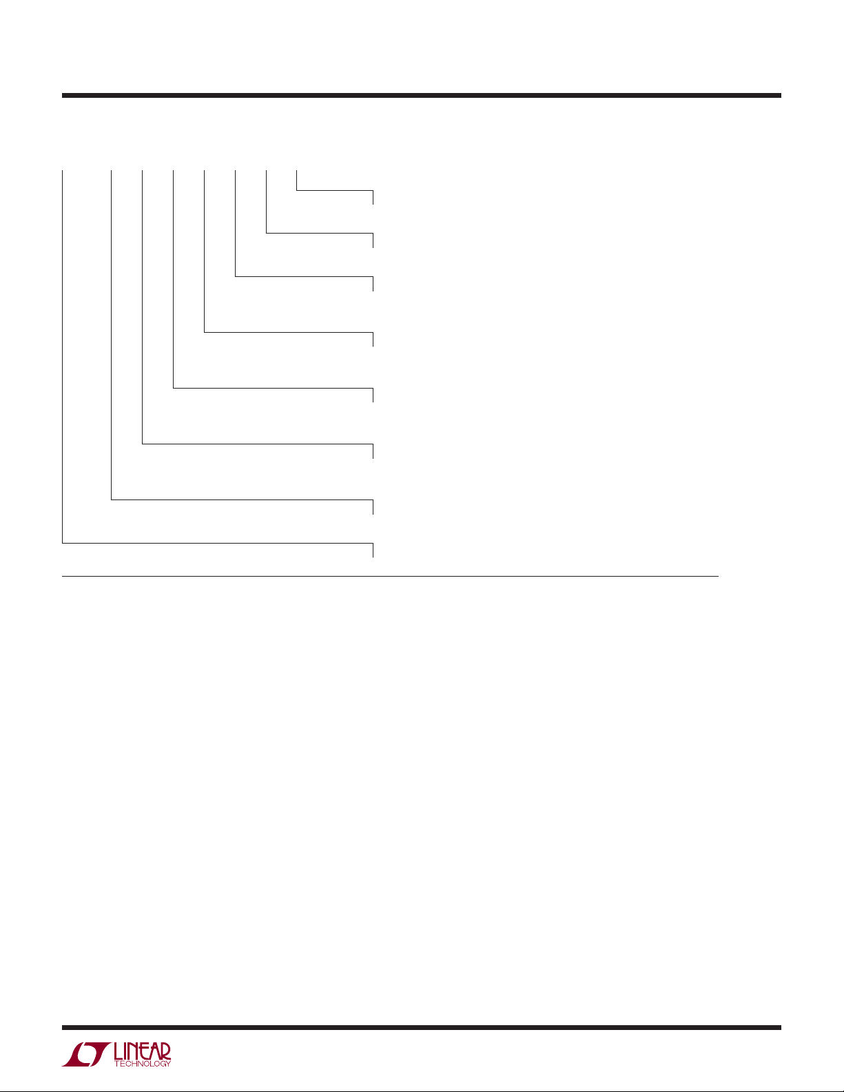
= 25°C. LTC2656B-L16/LTC2656-L12/LTC2656B-H16/LTC2656-H12 (see Figure 1).
A
l
4ns
l
4ns
l
9ns
l
9ns
l
10 ns
l
7ns
l
7ns
= 10pF
LOAD
V
= 4.5V to 5.5V
CC
V
= 2.7V to 4.5V
CC
l
l
l
20 ns
l
7ns
l
15 ns
l
200 ns
l
20
45
50 MHz
ns
ns
Note 1: Stresses beyond those listed under Absolute Maximum Ratings
may cause permanent damage to the device. Exposure to any Absolute
Maximum Rating condition for extended periods may affect device
reliability and lifetime.
Note 2: All voltages are with respect to GND.
Note 3: Linearity and monotonicity are defi ned from code kL to code
N
2
– 1, where N is the resolution and kL is the lower end code for which
no output limiting occurs. For V
linearity is defi ned from code 128 to code 65535. For V
= 2.5V and N = 16, kL = 128 and
REF
= 2.5V and
REF
N = 12, kL = 8 and linearity is defi ned from code 8 to code 4,095.
Note 4: Inferred from measurement at code 128 (LTC2656-16) or code 8
(LTC2656-12).
Note 5: DC crosstalk is measured with V
= 5V and using internal
CC
reference with the measured DAC at mid-scale.
Note 6: This IC includes current limiting that is intended to protect the
device during momentary overload conditions. Junction temperature can
exceed the rated maximum during current limiting. Continuous operation
above the specifi ed maximum operating junction temperature may impair
device reliability.
Note 7: Temperature coeffi cient is calculated by dividing the maximum
change in output voltage by the specifi ed temperature range.
Note 8: Digital inputs at 0V or V
CC
.
Note 9: Guaranteed by design and not production tested.
Note 10: Internal reference mode. DAC is stepped 1/4 scale to 3/4 scale
and 3/4 scale to 1/4 scale. Load is 2k in parallel with 200pF to GND.
Note 11: V
= 5V, internal reference mode. DAC is stepped ±1LSB
CC
between half scale and half scale – 1LSB. Load is 2k in parallel with 200pF
to GND.
Note 12: DAC-to-DAC crosstalk is the glitch that appears at the output
of one DAC due to a full-scale change at the output of another DAC. It is
measured with V
= 5V and using internal reference, with the measured
CC
DAC at mid-scale.
2656p
9
Page 10

LTC2656
TYPICAL PERFORMANCE CHARACTERISTICS
LTC2656-L16
Integral Nonlinearity (INL) Differential Nonlinearity (DNL) INL vs Temperature
4
3
2
1
0
INL (LSB)
–1
–2
–3
–4
128
1.0
= 3V
0.5
0
DNL (LSB)
–0.5
–1.0
128
V
CC
16384
32768
CODE
49152
65535
2656 G02
V
= 3V
CC
16384
32768
CODE
49152
65535
2656 G01
4
VCC = 3V
3
2
1
0
INL (LSB)
–1
–2
–3
–4
–30 130
–50
DNL vs Temperature REFOUT Voltage vs Temperature
(V)
REF
V
1.253
1.252
1.251
1.250
1.249
1.248
VCC = 3V
1.0
0.5
0
DNL (LSB)
–0.5
VCC = 3V
DNL (POS)
DNL (NEG)
INL (POS)
INL (NEG)
–10
30
10
TEMPERATURE (°C)
50
110
70
90
2656 G03
–1.0
CS/LD
3V/DIV
V
OUT
100µV/DIV
30
–30 130
–50
–10
TEMPERATURE (°C)
50
10
70
90
110
2656 G04
1.247
–30 10
–50
–10
30
TEMPERATURE (°C)
50 130
Settling to ±1LSB Rising Settling to ±1LSB Falling
3/4 SCALE TO 1/4
SCALE STEP
= 3V, VFS = 2.5V
V
CC
= 2k, CL = 200pF
R
L
AVERAGE OF 2048
EVENTS
2µs/DIV
1/4 SCALE TO 3/4
SCALE STEP
= 3V, VFS = 2.5V
V
CC
= 2k, CL = 200pF
R
L
AVERAGE OF 2048
EVENTS
2µs/DIV
8.9µs
2656 G06
V
OUT
100µV/DIV
CS/LD
3V/DIV
70
8.7µs
90
110
2656 G05
2656 G07
2656p
10
Page 11

LTC2656
TYPICAL PERFORMANCE CHARACTERISTICS
LTC2656-H16
Integral Nonlinearity (INL) Differential Nonlinearity (DNL) INL vs Temperature
4
3
2
1
0
INL (LSB)
–1
–2
–3
–4
128
1.0
= 5V
0.5
0
DNL (LSB)
–0.5
–1.0
128
V
CC
16384
32768
CODE
49152
65535
2656 G09
V
= 5V
CC
16384
32768
CODE
49152
65535
2656 G08
4
VCC = 5V
3
2
1
0
INL (LSB)
–1
–2
–3
–4
–30 130
–50
DNL vs Temperature REFOUT Voltage vs Temperature
1.0
0.5
0
DNL (LSB)
–0.5
VCC = 5V
DNL (POS)
DNL (NEG)
2.054
2.052
2.050
(V)
2.048
REF
V
2.046
2.044
VCC = 5V
INL (POS)
INL (NEG)
–10
30
10
TEMPERATURE (°C)
50
110
70
90
2656 G10
–1.0
CS/LD
5V/DIV
V
OUT
250µV/DIV
30
–30 130
–50
–10
TEMPERATURE (°C)
50
10
70
110
90
2656 G11
2.042
–30 10
–50
–10
30
TEMPERATURE (°C)
50 130
Settling to ±1LSB Rising Settling to ±1LSB Falling
6.1µs
3/4 SCALE TO 1/4
SCALE STEP
= 5V, VFS = 4.096V
V
CC
= 2k, CL = 200pF
R
L
AVERAGE OF 2048
EVENTS
2µs/DIV
1/4 SCALE TO
3/4 SCALE STEP
= 5V,
V
CC
= 4.096V
V
FS
7.9µs
RL = 2k, CL = 200pF
AVERAGE OF 2048
EVENTS
2µs/DIV
2656 G13
V
OUT
250µV/DIV
CS/LD
5V/DIV
90
110
70
2656 G12
2656 G14
2656p
11
Page 12

LTC2656
TYPICAL PERFORMANCE CHARACTERISTICS
LTC2656-12
Integral Nonlinearity (INL) Differential Nonlinearity (DNL) Settling to ±1LSB (12 Bit) Rising
1.0
0.5
VCC = 5V
= 2.048V
V
REF
1.0
0.5
VCC = 5V
= 2.048V
V
REF
CS/LD
5V/DIV
4.6µs
0
INL (LSB)
–0.5
–1.0
8
1024
2048
CODE
3072
4095
2656 G15
0
DNL (LSB)
–0.5
–1.0
8
LTC2656-16
Load Regulation Current Limiting
(mV)
OUT
∆V
–10
10
–2
–4
–6
–8
VCC = 5V (LTC2656-H)
8
V
6
INTERNAL REF.
CODE = MID-SCALE
4
2
0
–50
= 3V (LTC2656-L)
CC
–30–40
–10–20
I
OUT
10 20 40
0
(mA)
30
50
2656 G18
0.20
0.15
0.10
0.05
(V)
OUT
∆V
–0.05
–0.10
–0.15
–0.20
0
–50
1024
VCC = 5V (LTC2656-H)
V
CC
INTERNAL REF.
CODE = MID-SCALE
–30–40
2048
CODE
= 3V (LTC2656-L)
–10–20
0
I
(mA)
OUT
3072
10 20 40
30
2656 G16
2656 G19
4095
50
V
OUT
1mV/DIV
1/4 SCALE TO
3/4 SCALE STEP
= 5V,
V
CC
= 4.095V
V
FS
Headroom at Rails vs
Output Current
5.0
4.5
4.0
3V SOURCING
3.5
(LTC2656-L)
3.0
(V)
2.5
OUT
V
2.0
1.5
1.0
3V SINKING
0.5
(LTC2656-L)
0
21
0
RL = 2k, CL = 200pF
AVERAGE OF 2048
EVENTS
2µs/DIV
5V SOURCING
67 9
43
5
I
(mA)
OUT
2656 G17
5V
SINKING
8
10
2656 G20
Offset Error vs Temperature Zero-Scale Error vs Temperature Gain Error vs Temperature
1.00
0.75
0.50
0.25
0
–0.25
OFFSET ERROR (mV)
–0.50
–0.75
–1.00
–50
12
30
–30 130
–10
TEMPERATURE (°C)
50
10
110
70
90
3656 G21
3.0
2.5
2.0
1.5
1.0
ZERO-SCALE ERROR (mV)
0.5
0
–30 10
–50
–10
TEMPERATURE (°C)
90
50 130
70
30
110
2656 G22
64
48
32
16
0
–16
GAIN ERROR (LSB)
–32
–48
–64
–30 130
–50
–10
30
50
10
TEMPERATURE (°C)
110
70
90
2656 G23
2656p
Page 13

LTC2656
TYPICAL PERFORMANCE CHARACTERISTICS
LTC2656-16
Offset Error vs Reference Input Gain Error vs Reference Input ICC Shutdown vs V
2.0
VCC = 5.5V
OFFSET ERROR OF 8 CHANNELS
1.5
1.0
0.5
0
–0.5
OFFSET ERROR (mV)
–1.0
–1.5
–2.0
0.5
1.0
REFERENCE VOLTAGE (V)
1.5
2.0
2.5
2656 G24
64
VCC = 5.5V
GAIN ERROR OF 8 CHANNELS
48
32
16
0
–16
GAIN ERROR (LSBs)
–32
–48
–64
0.5
1.0
1.5
REFERENCE VOLTAGE (V)
2.0
2656 G25
2.5
450
400
350
300
250
(nA)
CC
200
I
150
100
50
0
2.5
3.0
3.5
Supply Current vs Logic Voltage Hardware CLR to Mid-Scale Hardware CLR to Zero-Scale
4.0
SWEEP SCK, SDI, CS/LD
BETWEEN 0V AND V
3.6
3.2
(mA)
CC
I
2.8
CC
VCC = 5V
(LTC2656-H)
V
OUT
1V/DIV
VCC = 5V
= 2.048V
V
REF
CODE = FULL-SCALE
V
OUT
1V/DIV
CC
4.0 5.5
4.5
= 2.048V
REF
5.0
VCC (V)
VCC = 5V
V
CODE = FULL-SCALE
2656 G26
2.4
2.0
VCC = 3V
(LTC2656-L)
1
0
LOGIC VOLTAGE (V)
3
4
2
5
2656 G27
CLR
5V/DIV
Multiplying Bandwidth Large-Signal Response
8
6
4
2
0
–2
–4
MAGNITUDE (dB)
–6
VCC = 5V
–8
V
REF(DC)
V
–10
REF(AC)
CODE = FULL-SCALE
–12
1k
= 2V
= 0.2V
P-P
10k 100k 1M
FREQUENCY (Hz)
2656 G30
V
OUT
1V/DIV
VCC = 5V
= 2.048V
V
REF
ZERO-SCALE TO FULL-SCALE
1µs/DIV
2.5μs/DIV
2656 G28
2656 G31
CLR
5V/DIV
Mid-Scale Glitch Impulse
CS/LD
5V/DIV
V
OUT
5mV/DIV
V
OUT
5mV/DIV
1µs/DIV
2656 G29
VCC = 5V, 6nV•s TYP
(LTC2656-H16)
VCC = 3V, 3nV•s TYP
(LTC2656-L16)
2µs/DIV
2656 G32
2656p
13
Page 14

LTC2656
TYPICAL PERFORMANCE CHARACTERISTICS
DAC-to-DAC Crosstalk (Dynamic) Power-On Reset Glitch Power-On Reset to Mid-Scale
ONE DAC
SWITCH 0-FS
2V/DIV
V
OUT
2mV/DIV
V
OUT
2mV/DIV
LTC2656-H16, VCC = 5V, 3nV•s TYP
LTC2656-H16, VCC = 5V, <1nV•s TYP
C
REFCOMP
C
REFCOMP
= C
= C
2µs/DIV
REFOUT
REFOUT
= NO LOAD
= 0.1µF
2656 G32
Noise Voltage vs Frequency 0.1Hz to 10Hz Voltage Noise
1200
1000
800
VCC = 5V
CODE = MID-SCALE
INTERNAL REF
= C
C
REFCOMP
REFOUT
= 0.1µF
V
CC
2V/DIV
V
OUT
10mV/DIV
VCC = 5V, VFS = 2.5V
CODE = MID-SCALE
INTERNAL REF
C
REFCOMP
= C
REFOUT
ZERO-SCALE
200µs/DIV
= 0.1µF
LTC2656
2656 G34
LTC2656-H
V
CC
2V/DIV
V
OUT
1V/DIV
Reference 0.1Hz to 10Hz
Voltage Noise
V
= 1.25V
REFOUT
= C
C
REFCOMP
REFOUT
250µs/DIV
2656 G35
= 0.1µF
600
400
NOISE VOLTAGE (nV/√Hz)
200
0
LTC2656-H
LTC2656-L
110
100 1k 10k 100k 1M
FREQUENCY (Hz)
2656 G36
5µV/DIV
1 SEC/DIV
2656 G37
2µV/DIV
1 SEC/DIV
2656 G38
14
2656p
Page 15

LTC2656
PIN FUNCTIONS
REFLO (Pin 1/Pin 19):
at this pin sets the zero-scale voltage of all DACs. REFLO
should be tied to GND.
V
to V
OUTA
20, 1, 3, 4, 13, 14, 15, 16):
puts. The output range is 0V to 2 times the voltage at the
REFIN/OUT pin.
REFCOMP (Pin 4/Pin 2):
tion Pin. For low noise and reference stability, tie a 0.1µF
capacitor to GND. Connect REFCOMP to GND to allow the
use of external reference at start-up.
REFIN/OUT (Pin 7/Pin 5):
reference output in internal reference mode and acts as
the reference input pin in external reference mode. When
acting as an output, the nominal voltage at this pin is
1.25V for L options and 2.048V for H options. For low
noise and reference stability tie a capacitor from this pin
to GND. This capacitor value must be ≤C
C
REFCOMP
external reference mode, the allowable reference input
voltage range is 0.5V to V
LDAC
(Pin 8/Pin 6):
CS/LD is high, a falling edge on LDAC immediately updates
the DAC register with the contents of the input register
(similar to a software update). If CS/LD is low when LDAC
goes low, the DAC register is updated after CS/LD returns
high. A low on the LDAC pin powers up the DAC outputs.
All the software power-down commands are ignored if
LDAC is low when CS/LD goes high.
CS/LD (Pin 9/Pin 7):
Input. When CS/LD is low, SCK is enabled for shifting
data on SDI into the register. When CS/LD is taken high,
SCK is disabled and the specifi ed command (see Table 1)
is executed.
(Pins 2, 3, 5, 6, 15, 16, 17, 18/Pins
OUTH
is the capacitance tied to the REFCOMP pin. In
(TSSOP/QFN)
Reference Low Pin. The voltage
DAC Analog Voltage Out-
Internal Reference Compensa-
This pin acts as the internal
REFCOMP ,
/2.
CC
Asynchronous DAC Update Pin. If
Serial Interface Chip Select/Load
where
SCK (Pin 10/Pin 8):
and TTL compatible.
SDI (Pin 11/Pin 9):
applied to SDI for transfer to the device at the rising edge
of SCK (Pin 10). The LTC2656 accepts input word lengths
of either 24 or 32 bits.
SDO (Pin 12/Pin 10):
pin is used for daisy-chain operation.
of the shift register appears at the SDO pin. The data
transferred to the device via the SDI pin is delayed 32
SCK rising edges before being output at the next falling
edge. This pin is continuously driven and does not go high
impedance when CS/LD is taken active high.
CLR (Pin 13/Pin 11):
low at this level-triggered input clears all registers and
causes the DAC voltage outputs to drop to 0V if the PORSEL
pin is tied to GND. If the PORSEL pin is tied to V
low at CLR sets all registers to mid-scale code and causes
the DAC voltage outputs to go to mid-scale.
PORSEL (Pin 14/Pin 12):
tied to GND, the DAC resets to zero-scale at power-up. If
tied to V
VCC (Pin 19/Pin 17):
tions, 2.7V ≤ V
≤ 5.5V.
GND (Pin 20/Pin 18):
Exposed Pad (Pin 21/Pin 21):
to PCB Ground.
, the DAC resets to mid-scale at power-up.
CC
Serial Interface Clock Input. CMOS
Serial Interface Data Input. Data is
Serial Interface Data Output. This
The serial output
Asynchronous Clear Input. A logic
, a logic
CC
Power-On Reset Select Pin. If
Supply Voltage Input. For -L op-
≤ 5.5V and for -H options, 4.5V ≤ VCC
CC
Ground.
Ground. Must be soldered
2656p
15
Page 16

LTC2656
BLOCK DIAGRAM
REFCOMP REFIN/OUT
GND
REFLO
V
OUTA
V
OUTB
V
OUTC
V
OUTD
CS/LD
SCK
LDAC
REF
DAC A
REF
DAC B
REF
DAC C
REF
DAC D
INTERNAL REFERENCE
REGISTER
REGISTER
REGISTER
REGISTER
REGISTER
REGISTER
REGISTER
REGISTER
32-BIT SHIFT REGISTER
DECODECONTROL LOGIC
REGISTER
REGISTER
REGISTER
REGISTER
DAC H V
REGISTER
DAC G V
REGISTER
DAC F V
REGISTER
DAC E V
REGISTER
POWER-ON RESET
REF
REF
REF
REF
V
CC
OUTH
OUTG
OUTF
OUTE
PORSEL
SDO
SDI
CLR
2656 BD
TIMING DIAGRAMS
SCK
SDI
t
5
CS/LD
SDO
LDAC
t
1
t
2
12 3
t
7
t
t
3
4
23 24
t
8
Figure 1a
CS/LD
t
13
LDAC
2656 F01b
t
6
t
10
t
t
13
12
2656 F01a
Figure 1b
2656p
16
Page 17

OPERATION
LTC2656
The LTC2656 is a family of octal voltage output DACs in
20-lead 4mm × 5mm QFN and in 20-lead thermally enhanced TSSOP packages. Each DAC can operate rail-to-rail
in external reference mode, or with its full-scale voltage
set by an integrated reference. Four combinations of accuracy (16-bit and 12-bit), and full-scale voltage (2.5V or
4.096V) are available. The LTC2656 is controlled using a
4-wire SPI/MICROWIRE compatible interface.
Power-On Reset
The LTC2656-L/ LTC2656-H clear the output to zero scale if
the PORSEL pin is tied to GND, when power is fi rst applied,
making system initialization consistent and repeatable. For
some applications, downstream circuits are active during
DAC power-up and may be sensitive to nonzero outputs
from the DAC during this time. The LTC2656 contains
circuitry to reduce the power-on glitch. The analog outputs
typically rise less than 10mV above zero scale during power
on if the power supply is ramped to 5V in 1ms or more.
In general, the glitch amplitude decreases as the power
supply ramp time is increased. See Power-On Reset Glitch
in the Typical Performance Characteristics.
Alternatively, if the PORSEL pin is tied to V
, the
CC
LTC2656-L/ LTC2656-H sets the output to mid-scale when
power is fi rst applied.
Power Supply Sequencing and Start-Up
For the LTC2656 family of parts, the internal reference is
powered up at start-up by default. If an external reference
is to be used, the REFCOMP pin must be hardwired to
GND. Having REFCOMP hardwired to GND at power up
will cause the REFIN/OUT pin to become high impedance
and will allow for the use of an external reference at startup. However in this confi guration, the internal reference
will still be on even though it is disconnected from the
REFIN/OUT pin and will draw supply current. In order
to use external reference after power-up, the command
Select External Reference (0111b) should be used to turn
the internal reference off (see Table 1.)
supply turn-on and turn-off sequences, when the voltage
is in transition.
at V
CC
Transfer Function
The digital-to-analog transfer function is:
⎛
⎞
V
OUT IDEAL
k
⎜
⎟
N
⎝
⎠
2
VV V
•• –=
2
()
REF REFLO REFL()
+
OO
where k is the decimal equivalent of the binary DAC input
code, N is the resolution of the DAC, and V
is the volt-
REF
age at the REFIN/OUT pin. The resulting DAC output span
is 0V to 2 • V
is nominally 1.25V for LTC2656-L and 2.048V for
V
REF
, as it is necessary to tie REFLO to GND.
REF
LTC2656-H, in internal reference mode.
Table 1. Command and Adress Codes
COMMAND*
C3 C2 C1 C0
0 0 0 0 Write to Input Register n
0 0 0 1 Update (Power Up) DAC Register n
0 0 1 0 Write to Input Register n, Update (Power Up) All
0 0 1 1 Write to and Update (Power Up) n
0 1 0 0 Power Down n
0 1 0 1 Power Down Chip (All DACs and Reference)
0 1 1 0 Select Internal Reference (Power-Up Reference)
0 1 1 1 Select External Reference (Power-Down
1 1 1 1 No Operation
ADDRESS (n)*
A3 A2 A1 A0
0 0 0 0 DAC A
0 0 0 1 DAC B
0 0 1 0 DAC C
0 0 1 1 DAC D
0 1 0 0 DAC E
0 1 0 1 DAC F
0 1 1 0 DAC G
0 1 1 1 DAC H
1 1 1 1 All DACs
*Command and address codes not shown are reserved and should not
be used.
Reference)
Serial Interface
The voltage at REFIN/OUT should be kept within the range
– 0.3V ≤ REFIN/OUT ≤ V
+ 0.3V if the external reference
CC
is to be used (see Absolute Maximum Ratings). Particular
care should be taken to observe these limits during power
The CS/LD input is level triggered. When this input is taken
low, it acts as a chip-select signal, powering on the SDI
and SCK buffers and enabling the input shift register. Data
(SDI input) is transferred at the next 24 rising SCK edges.
2656p
17
Page 18

LTC2656
OPERATION
The 4-bit command, C3-C0, is loaded fi rst; followed by the
4-bit DAC address, A3-A0; and fi nally the 16-bit data word.
For the LTC2656-16 the data word comprises the 16-bit
input code, ordered MSB-to-LSB. For the LTC2656-12 the
data word comprizes the 12-bit input code, ordered MSBto-LSB, followed by four don’t care bits. Data can only be
transferred to the LTC2656 when the CS/LD signal is low.
The rising edge of CS/LD ends the data transfer and causes
the device to carry out the action specifi ed in the 24-bit input
word. The complete sequence is shown in Figure 2a.
The command (C3-C0) and address (A3-A0) assignments
are shown in Table 1. The fi rst four commands in the table
consist of write and update operations. A write operation
loads a 16-bit data word from the 32-bit shift register
into the input register of the selected DAC, n. An update
operation copies the data word from the input register to
the DAC register. Once copied into the DAC register, the
data word becomes the active 16- or 12-bit input code,
and is converted to an analog voltage at the DAC output.
The update operation also powers up the selected DAC
if it had been in power-down mode. The data path and
registers are shown in the Block Diagram.
While the minimum input word is 24 bits, it may optionally be extended to 32 bits. To use the 32-bit word width,
8 don’t-care bits must be transferred to the device fi rst,
followed by the 24-bit word as just described. Figure 2b
shows the 32-bit sequence. The 32-bit word is required for
daisy-chain operation, and is also available to accommodate
microprocessors that have a minimum word width of 16 bits
(2 bytes). The 16-bit data word is ignored for all commands
that do not include a write operation.
Daisy-Chain Operation
The serial output of the shift register appears at the SDO pin.
Data transferred to the device from the SDI input is delayed
32 SCK rising edges before being output at the next SCK
falling edge. The SDO pin is continuously driven and does
not go high impedance when CS/LD is taken active high.
The SDO output can be used to facilitate control of multiple
serial devices from a single 3-wire serial port (i.e., SCK,
SDI and CS/LD). Such a “daisy-chain” series is confi gured
by connecting SDO of each upstream device to SDI of the
next device in the chain. The shift registers of the devices
are thus connected in series, effectively forming a single
input shift register which extends through the entire
chain. Because of this, the devices can be addressed and
controlled individually by simply concatenating their input
words; the fi rst instruction addresses the last device in
the chain and so forth. The SCK and CS/LD signals are
common to all devices in the series.
In use, CS/LD is fi rst taken low. Then the concatenated
input data is transferred to the chain, using SDI of the
fi rst device as the data input. When the data transfer is
complete, CS/LD is taken high, completing the instruction
sequence for all devices simultaneously. A single device
can be controlled by using the no-operation command
(1111) for the other devices in the chain.
Power-Down Mode
For power-constrained applications, power-down mode
can be used to reduce the supply current whenever
less than eight DAC outputs are needed. When in power
down, the buffer amplifi ers, bias circuits and integrated
reference circuits are disabled and draw essentially zero
current. The DAC outputs are put into a high impedance
state, and the output pins are passively pulled to ground
through individual 80k resistors. Input- and DAC-register
contents are not disturbed during power down.
Any channel or combination of DAC channels can be put
into power-down mode by using command 0100b in
combination with the appropriate DAC address, (n). The
integrated reference is automatically powered down when
external reference is selected using command 0111b. In
addition, all the DAC channels and the integrated reference together can be put into power-down mode using
power-down chip command 0101b. For all power-down
commands the 16-bit data word is ignored.
Normal operation resumes by executing any command
which includes a DAC update, in software as shown in
Table 1 or by taking the asynchronous LDAC pin low. The
selected DAC is powered up as its voltage output is updated. When a DAC which is in a powered-down state is
powered up and updated, normal settling is delayed. If less
than eight DACs are in a powered-down state prior to the
update command, the power-up delay time is 12µs. If, on
the other hand, all eight DACs and the integrated reference
2656p
18
Page 19

OPERATION
24
23
2656 F02a
32-BIT
CURRENT
INPUT WORD
LTC2656
2656 F02b
22
21
20
19
18
17
16
15
14
13
12
COMMAND WORD ADDRESS WORD DATA WORD
24-BIT INPUT WORD
Figure 2a. LTC2656-16 24-Bit Load Sequence (Minimum Input Word)
LTC2656-12 SDI Data Word: 12-Bit Input Code + 4 Don’t-Care Bits
11
10
9
8
7
6
5
4
3
2
C2 C1 C0 A3 A2 A1 A0 D15 D14 D13 D12 D11 D10 D9 D8 D7 D6 D5 D4 D3 D2 D1 D0C3
1
24 25 26 27 28 29 30 31 32
23
22
21
20
19
18
17
16
15
14
13
12
11
10
C2 C1 C0 A3 A2 A1 A0 D15 D14 D13 D12 D11 D10 D9 D8 D7 D6 D5 D4 D3 D2 D1 D0C3XXXXXXXX
9
8
7
6
5
4
3
C2 C1 C0 A3 A2 A1 A0 D15 D14 D13 D12 D11 D10 D9 D8 D7 D6 D5 D4 D3 D2 D1 D0C3XXXXXXXX
COMMAND WORD ADDRESS WORD DATA WORD
DON’T CARE
18
D14
D15
SDI
PREVIOUS D14PREVIOUS D15
8
t
SDO
4
t
2
t
3
t
17
1
t
SCK
PREVIOUS 32-BIT INPUT WORD
Figure 2b. LTC2656-16 32-Bit Load Sequence
LTC2656-12 SDI/SDO Data Word: 12-Bit Input Code + 4 Don’t-Care Bits
CS/LD
SCK
SDI
CS/LD
2
1
SCK
SDI
SDO
2656p
19
Page 20

LTC2656
OPERATION
are powered down, then the main bias generation circuit
block has been automatically shut down in addition to the
individual DAC amplifi ers and integrated reference. In this
case, the power-up delay time is 14µs. The power up of
the integrated reference depends on the command that
powered it down. If the reference is powered down using
the select external reference command (0111b), then it can
only be powered back up using select internal reference
command (0110b). However if the reference was powered
down using power-down chip command (0101b), then in
addition to select internal reference command (0110b),
any command that powers up the DACs will also power
up the integrated reference.
Asynchronous DAC Update Using LDAC
In addition to the update commands shown in Table 1, the
LDAC pin asynchronously updates all the DAC registers
with the contents of the input registers.
If CS/LD is high, a low on the LDAC pin causes all the
DAC registers to be updated with the contents of the
input registers.
If CS/LD is low, a low going pulse on the LDAC pin before
the rising edge of CS/LD powers up all the DAC outputs but
does not cause the output to be updated. If LDAC remains
low after the rising edge of CS/LD, then LDAC is recognized,
the command specifi ed in the 24-bit word just transferred
is executed and the DAC outputs are updated.
The DAC outputs are powered up when LDAC is taken
low, independent of the state of CS/LD. The integrated
reference is also powered up if it was powered down using power-down chip (0101b) command. The integrated
reference will not power up when LDAC is taken low,
if it was powered down using select external reference
(0111b) command.
If LDAC is low at the time CS/LD goes high, it inhibits any
software power-down command (power down n, powerdown chip, select external reference) that was specifi ed
in the input word.
Reference Modes
reference. The LTC2656-L has a 1.25V reference that provides a full-scale DAC output of 2.5V. The LTC2656-H has
a 2.048V reference that provides a full-scale DAC output
of 4.096V. Both references exhibit a typical temperature
drift of 2ppm/°C. Internal reference mode can be selected
by using command 0110b, and is the power-on default. A
buffer is needed if the internal reference is required to drive
external circuitry. For reference stability and low noise, it
is recommended that a 0.1µF capacitor be tied between
REFCOMP and GND. In this confi guration, the internal
reference can drive up to 0.1µF capacitive load without any
stability problems. In order to ensure stable operation, the
capacitive load on the REFIN/OUT pin should not exceed
the capacitive load on the REFCOMP pin.
The DAC can also operate in external reference mode using command 0111b. In this mode, the REFIN/OUT pin
acts as an input that sets the DAC’s reference voltage. The
input is high impedance and does not load the external
reference source. The acceptable voltage range at this
pin is 0.5V ≤ REFIN/OUT ≤ V
output voltage is 2 • V
ence at start-up, see the Power Supply Sequencing and
Start-Up section.
Integrated Reference Buffers
Each of the eight DACs in LTC2656 has its own integrated
high performance reference buffer. The buffers have very
high input impedance and do not load the reference voltage
source. These buffers shield the reference voltage from
glitches caused by DAC switching and thus minimize DACto-DAC dynamic crosstalk. Typically DAC-to-DAC crosstalk
is less than 3nV•s. By tying 0.1µF capacitors between
REFCOMP and GND, and also between REFIN/OUT and
GND, this number can be reduced to less than 1nV•s. See
the curve DAC-to-DAC Dynamic Crosstalk in the Typical
Performance Characteristics section.
Voltage Outputs
Each of the LTC2656’s eight rail-to-rail output amplifi ers contained in these parts has a guaranteed load regulation when
sourcing or sinking up to 15mA at 5V (7.5mA at 3V).
REFIN/OUT
/2. The resulting full-scale
CC
. For using external refer-
For applications where an accurate external reference is
not available, the LTC2656 has a user-selectable, integrated
20
Load regulation is a measure of the amplifi er’s ability to
maintain the rated voltage accuracy over a wide range of
2656p
Page 21

OPERATION
LTC2656
load conditions. The measured change in output voltage
per milliampere of forced load current change is expressed
in LSB/mA.
DC output impedance is equivalent to load regulation, and
may be derived from it by simply calculating a change in
units from LSB/mA to Ohms. The amplifi ers’ DC output
impedance is 0.04 when driving a load well away from
the rails.
When drawing a load current from either rail, the output
voltage headroom with respect to that rail is limited by
the 30 typical channel resistance of the output devices;
e.g., when sinking 1mA, the minimum output voltage =
30 • 1mA = 30mV. See the graph Headroom at Rails vs
Output Current in the Typical Performance Characteristics
section.
The amplifi ers are stable driving capacitive loads of up
to 1000pF.
Board Layout
The excellent load regulation and DC crosstalk performance
of these devices is achieved in part by keeping “signal”
and “power” grounds separate.
The PC board should have separate areas for the analog
and digital sections of the circuit. This keeps digital signals
away from sensitive analog signals and facilitates the use of
separate digital and analog ground planes which have minimal capacitive and resistive interaction with each other.
Digital and analog ground planes should be joined at only
one point, establishing a system star ground as close to
the device’s ground pin as possible. Ideally, the analog
ground plane should be located on the component side of
the board, and should be allowed to run under the part to
shield it from noise. Analog ground should be a continuous
and uninterrupted plane, except for necessary lead pads
and vias, with signal traces on another layer.
The GND pin functions as a return path for power supply
currents in the device and should be connected to analog
ground. The REFLO pin should be connected to the system
star ground. Resistance from the REFLO pin to the system
star ground should be as low as possible.
Rail-to-Rail Output Considerations
In any rail-to-rail voltage output device, the output is limited
to voltages within the supply range.
Since the analog outputs of the device cannot go below
ground, they may limit the lowest codes as shown in Figure 3b. Similarly, limiting can occur in external reference
mode near full scale when the REFIN/OUT pin is at V
If V
REFIN/OUT
= VCC/2 and the DAC full-scale error (FSE)
is positive, the output for the highest codes limits at V
CC
/2.
CC
are shown in Figure 3c. No full-scale limiting can occur if
V
REFIN/OUT
≤ (VCC – FSE)/2.
Offset and linearity are defi ned and tested over the region
of the DAC transfer function where no output limiting can
occur.
VOLTAGE
NEGATIVE
OFFSET
V
REF
V
= V
REF
CC
OUTPUT
VOLTAGE
OUTPUT
32,7680 65,535
INPUT CODE
0V
Figure 3. Effects of Rail-to-Rail Operation on a DAC Transfer Curve. (3a) Overall Transfer Function (3b) Effect of
Negative Offset for Codes Near Zero-Scale (3c) Effect of Positive Full-Scale Error for Codes Near Full-Scale
INPUT CODE
(3b)
(3a)
= V
CC
INPUT CODE
(3c)
POSITIVE
FSE
OUTPUT
VOLTAGE
2656 F03
2656p
21
Page 22

LTC2656
PACKAGE DESCRIPTION
FE Package
20-Lead Plastic TSSOP (4.4mm)
(Reference LTC DWG # 05-08-1663)
Exposed Pad Variation CB
3.86
(.152)
6.60 p0.10
4.50 p0.10
RECOMMENDED SOLDER PAD LAYOUT
0.09 – 0.20
(.0035 – .0079)
NOTE:
1. CONTROLLING DIMENSION: MILLIMETERS
2. DIMENSIONS ARE IN
3. DRAWING NOT TO SCALE
SEE NOTE 4
0.65 BSC
4.30 – 4.50*
(.169 – .177)
0.50 – 0.75
(.020 – .030)
MILLIMETERS
(INCHES)
2.74
(.108)
0.45 p0.05
1.05 p0.10
0.25
REF
6.40 – 6.60*
(.252 – .260)
3.86
(.152)
20 1918 17 16 15
1345678910
2
0o – 8o
0.65
(.0256)
BSC
0.195 – 0.30
(.0077 – .0118)
TYP
4. RECOMMENDED MINIMUM PCB METAL SIZE
FOR EXPOSED PAD ATTACHMENT
*DIMENSIONS DO NOT INCLUDE MOLD FLASH. MOLD FLASH
SHALL NOT EXCEED 0.150mm (.006") PER SIDE
111214 13
2.74
(.108)
1.20
(.047)
MAX
0.05 – 0.15
(.002 – .006)
FE20 (CB) TSSOP 0204
6.40
(.252)
BSC
22
2656p
Page 23

PACKAGE DESCRIPTION
LTC2656
UFD Package
20-Lead Plastic QFN (4mm × 5mm)
(Reference LTC DWG # 05-08-1711 Rev B)
0.70 p0.05
4.50 p 0.05
3.10 p 0.05
1.50 REF
RECOMMENDED SOLDER PAD PITCH AND DIMENSIONS
APPLY SOLDER MASK TO AREAS THAT ARE NOT SOLDERED
5.00 p 0.10
(2 SIDES)
2.65 p 0.05
3.65 p 0.05
0.25 p0.05
0.50 BSC
2.50 REF
4.10 p 0.05
5.50 p 0.05
4.00 p 0.10
(2 SIDES)
PIN 1
TOP MARK
(NOTE 6)
PACKAGE OUTLINE
0.75 p 0.05
2.50 REF
R = 0.05 TYP
1.50 REF
3.65 p 0.10
2.65 p 0.10
PIN 1 NOTCH
R = 0.20 OR
C = 0.35
19 20
0.40 p 0.10
1
2
0.200 REF
0.00 – 0.05
NOTE:
1. DRAWING PROPOSED TO BE MADE A JEDEC PACKAGE OUTLINE MO-220 VARIATION (WXXX-X).
2. DRAWING NOT TO SCALE
3. ALL DIMENSIONS ARE IN MILLIMETERS
4. DIMENSIONS OF EXPOSED PAD ON BOTTOM OF PACKAGE DO NOT INCLUDE
MOLD FLASH. MOLD FLASH, IF PRESENT, SHALL NOT EXCEED 0.15mm ON ANY SIDE
5. EXPOSED PAD SHALL BE SOLDER PLATED
6. SHADED AREA IS ONLY A REFERENCE FOR PIN 1 LOCATION
ON THE TOP AND BOTTOM OF PACKAGE
Information furnished by Linear Technology Corporation is believed to be accurate and reliable.
However, no responsibility is assumed for its use. Linear Technology Corporation makes no representation that the interconnection of its circuits as described herein will not infringe on existing patent rights.
R = 0.115
TYP
BOTTOM VIEW—EXPOSED PAD
0.25 p 0.05
0.50 BSC
(UFD20) QFN 0506 REV B
2656p
23
Page 24

LTC2656
TYPICAL APPLICATION
Digitally Controlled Output Voltage 1.1A Supply
3
1
PORSEL
GNDREFLO
V
CC
C1
0.1µF
R4
1.2V TO 36V
7.5k
V
CC
V
V
V
V
V
V
V
V
OUTA
OUTB
OUTC
OUTD
OUTE
OUTF
OUTG
OUTH
20
1
3
4
13
14
15
16
MICROCONTROLLER
V
CC
JP2
MID-SCALE
ZERO-SCALE
C1
0.1µF
REFCOMP REFIN/OUT
7
CS
TO
8
SCK
10
SDO
9
SDI
*PIN NUMBERS INDICATED ARE FOR THE QFN PACKAGE
4
2
C1
0.1µF
LDAC CLR
LTC2656*
GND
21 19 18
RELATED PARTS
PART NUMBER DESCRIPTION COMMENTS
LTC1660/LTC1665 Octal 10-/8-Bit V
LTC1664 Quad 10-Bit V
LTC1821 Single 16-Bit V
LTC2600/LTC2610/
Octal 16-/14-/12-Bit V
LTC2620
LTC2601/LTC2611/
Single 16-/14-/12-Bit V
LTC2621
LTC2602/LTC2612/
Dual 16-/14-/12-Bit V
LTC2622
LTC2604/LTC2614/
Quad 16-/14-/12-Bit V
LTC2624
LTC2605/LTC2615/
Octal 16-/14-/12-Bit V
LTC2625
LTC2606/LTC2616/
Single 16-/14-/12-Bit V
LTC2626
LTC2609/LTC2619/
Quad 16-/14-/12-Bit V
LTC2629
LTC2636 Octal 12-/10-/8-Bit V
LTC2641/LTC2642 Single 16-/14-/12-Bit V
LTC2704 Quad 16-/14-/12-Bit V
±1LSB DNL
LTC2755 Quad 16-/14-/12-Bit I
±1LSB DNL
DACs in 16-Pin Narrow SSOP VCC = 2.7V to 5.5V, Micropower, Rail-to-Rail Output
OUT
DAC in 16-Pin Narrow SSOP VCC = 2.7V to 5.5V, Micropower, Rail-to-Rail Output
OUT
DAC with ±1LSB INL, DNL Parallel Interface, Precision 16-Bit Settling in 2s for 10V Step
OUT
DACs in 16-Lead Narrow SSOP 250A per DAC, 2.5V to 5.5V Supply Range, Rail-to-Rail Output,
OUT
SPI Serial Interface
DACs in 10-Lead DFN 300A per DAC, 2.5V to 5.5V Supply Range, Rail-to-Rail Output,
OUT
SPI Serial Interface
DACs in 8-Lead MSOP 300A per DAC, 2.5V to 5.5V Supply Range, Rail-to-Rail Output,
OUT
SPI Serial Interface
DACs in 16-Lead SSOP 250A per DAC, 2.5V to 5.5V Supply Range, Rail-to-Rail Output,
OUT
SPI Serial Interface
DACs with I2C Interface 250A per DAC, 2.7V to 5.5V Supply Range, Rail-to-Rail Output
OUT
DACs with I2C Interface 270A per DAC, 2.7V to 5.5V Supply Range, Rail-to-Rail Output
OUT
DACs with I2C Interface 250A per DAC, 2.7V to 5.5V Supply Range, Rail-to-Rail Output with
OUT
Separate V
DACs with 10ppm/°C Reference 125A per DAC, 2.7V to 5.5V Supply Range, Internal 1.25V or 2.048V
OUT
Reference, Rail-to-Rail Output, SPI Interface
DACs with ±1LSB INL, DNL ±1LSB (Max) INL, DNL, 3mm x 3mm DFN and MSOP Packages,
OUT
120A Supply Current, SPI Interface
DACs with ±2LSB INL,
OUT
DACs with ±1LSB INL,
OUT
Software Programmable Output Ranges Up to ±10V, SPI Interface
Software Programmable Output Ranges Up to ±10V, Parallel Interface
V
IN
LT3080
V
CONTROL
IN
+
1µF
NOTE: LT3080 MINIMUM LOAD CURRENT
IS 0.5mA
Pins for Each DAC
REF
–
SET
OUT
V
OUT
2.2µF
2656 TA02
24
Linear Technology Corporation
1630 McCarthy Blvd., Milpitas, CA 95035-7417
(408) 432-1900 ● FAX: (408) 434-0507
●
www.linear.com
2656p
LT 0409 • PRINTED IN USA
© LINEAR TECHNOLOGY CORPORATION 2009
 Loading...