

Page 1
Ultra-Tiny, Differential,
16-Bit ΔΣ ADC With
FEATURES DESCRIPTION
■
±VCC Differential Input Range
■
16-Bit Resolution (Including Sign), No Missing
Codes
■
2LSB Offset Error
■
4LSB Full-Scale Error
■
60 Conversions Per Second
■
Single Conversion Settling Time for Multiplexed
Applications
■
Single-Cycle Operation with Auto Shutdown
■
800μA Supply Current
■
0.2μA Sleep Current
■
Internal Oscillator—No External Components
Required
■
2-Wire I2C Interface
■
Ultra-Tiny 8-Pin 3mm × 2mm DFN
and TSOT23 Packages
APPLICATIONS
■
System Monitoring
■
Environmental Monitoring
■
Direct Temperature Measurements
■
Instrumentation
■
Industrial Process Control
■
Data Acquisition
■
Embedded ADC Upgrades
, LT, LTC and LTM are registered trademarks of Linear Technology Corporation.
All other trademarks are the property of their respective owners.
Protected by U.S. Patents, including 6208279, 6411242, 7088280, 7164378.
The LTC®2453 is an ultra-tiny, fully differential, 16-bit,
analog-to-digital converter. The LTC2453 uses a single
2.7V to 5.5V supply and communicates through an I
interface. The ADC is available in an 8-pin, 3mm × 2mm
DFN package or 8-pin, 3mm × 3mm TSOT package. It
includes an integrated oscillator that does not require any
external components. It uses a delta-sigma modulator
as a converter core and has no latency for multiplexed
applications. The LTC2453 includes a proprietary input
sampling scheme that reduces the average input sampling current several orders of magnitude lower than
conventional delta-sigma converters. Additionally, due
to its architecture, there is negligible current leakage
between the input pins.
The LTC2453 can sample at 60 conversions per second,
and due to the very large oversampling ratio, has ex-tremely
relaxed antialiasing requirements. The LTC2453 includes
continuous internal offset and full-scale calibration algorithms which are transparent to the user, ensuring accuracy
over time and over the operating temperature range. The
converter has external REF
input voltage range can extend up to ±(V
Following a single conversion, the LTC2453 can automatically enter a sleep mode and reduce its power to less
than 0.2μA. If the user reads the ADC once a second, the
LTC2453 consumes an average of less than 50μW from
a 2.7V supply.
LTC2453
2
I
C Interface
+
and REF– pins and the differential
REF
+
– V
REF
–
).
2
C
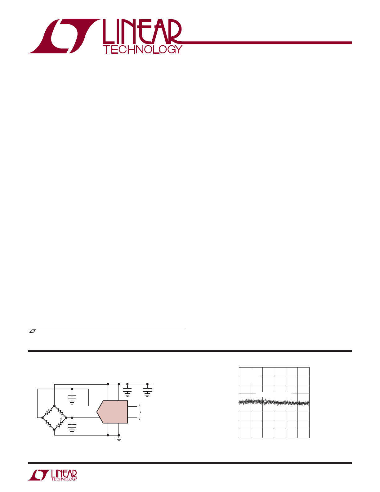
TYPICAL APPLICATION
IN
IN
REF+V
+
–
REF
LTC2453
–
CC
GND
2453 TA01
10k
10k
10k
R
0.1μF
0.1μF
0.1μF 10μF
SCL
2-WIRE I2C
SDA
INTERFACE
2.7V TO 5.5V
Integral Nonlinearity, VCC = 3V
2.0
VCC = 3V
+
= 3V
V
REF
1.5
–
V
= 0V
REF
1.0
0.5
0
INL (LSB)
–0.5
–1.0
–1.5
–2.0
–3
TA = –45°C, 25°C, 90°C
–2 –1 1
DIFFERENTIAL INPUT VOLTAGE (V)
0
2
3
2453fa
1
Page 2
LTC2453
ABSOLUTE MAXIMUM RATINGS
(Notes 1, 2)
Supply Voltage (VCC) ................................... –0.3V to 6V
+
–
, V
Analog Input Voltage (V
Reference Voltage (V
REF
IN
+
, V
) .. –0.3V to (V
IN
–
) .. –0.3V to (V
REF
Digital Voltage (SDA, SCL) ............ –0.3V to (V
+ 0.3V)
CC
+ 0.3V)
CC
+ 0.3V)
CC
PIN CONFIGURATION
TOP VIEW
Storage Temperature Range ................... –65°C to 150°C
Operating Temperature Range
LTC2453C ................................................ 0°C to 70°C
LTC2453I.............................................. –40°C to 85°C
SDA
1GND
–
REF
2
+
REF
3
V
4
CC
8-LEAD (3mm × 2mm) PLASTIC DFN
C/I GRADE T
EXPOSED PAD (PIN 9) IS GND, MUST BE SOLDERED TO PCB
DDB PACKAGE
JMAX
8
SCL
7
9
= 125°C, θJA = 76°C/W
+
IN
6
–
IN
5
GND 1
REF¯ 2
REF
VCC4
C/I GRADE T
TOP VIEW
8 SDA
+
3
TS8 PACKAGE
8-LEAD PLASTIC TSOT-23
= 125°C, θJA = 140°C/W
JMAX
7 SCL
6 IN
5 IN¯
+
ORDER INFORMATION
Lead Free Finish
TAPE AND REEL (MINI) TAPE AND REEL PART MARKING* PACKAGE DESCRIPTION TEMPERATURE RANGE
LTC2453CDDB#TRMPBF LTC2453CDDB#TRPBF LDBQ
LTC2453IDDB#TRMPBF LTC2453IDDB#TRPBF LDBQ
LTC2453CTS8#TRMPBF LTC2453CTS8#TRPBF LTDCG 8-Lead Plastic TSOT-23 0°C to 70°C
LTC2453ITS8#TRMPBF LTC2453ITS8#TRPBF LTDCG 8-Lead Plastic TSOT-23 –40°C to 85°C
TRM = 500 pieces. *Temperature grades are identifi ed by a label on the shipping container.
Consult LTC Marketing for parts specifi ed with wider operating temperature ranges.
Consult LTC Marketing for information on lead based fi nish parts.
For more information on lead free part marking, go to: http://www.linear.com/leadfree/
For more information on tape and reel specifi cations, go to: http://www.linear.com/tapeandreel/
8-Lead Plastic (3mm × 2mm) DFN
8-Lead Plastic (3mm × 2mm) DFN
0°C to 70°C
–40°C to 85°C
ELECTRICAL CHARACTERISTICS
The l denotes the specifi cations which apply over the full operating
temperature range, otherwise specifi cations are at TA = 25°C. (Note 2)
PARAMETER CONDITIONS MIN TYP MAX UNITS
l
Resolution (No Missing Codes) (Note 3)
Integral Nonlinearity (Note 4)
Offset Error
Offset Error Drift 0.02 LSB/°C
Gain Error
Gain Error Drift 0.02 LSB/°C
Transition Noise 1.4 μV
Power Supply Rejection DC 80 dB
16 Bits
l
l
l
210 LSB
210 LSB
0.01 0.02 % of FS
RMS
2453fa
2
Page 3

LTC2453
The l denotes the specifi cations which apply over the full
ANALOG INPUTS AND REFERENCES
operating temperature range, otherwise specifi cations are at T
SYMBOL PARAMETER CONDITIONS MIN TYP MAX UNITS
+
V
IN
–
V
IN
+
V
REF
–
V
REF
+
, V
V
OR
UR
–
, V
V
OR
UR
C
IN
I
DC_LEAK(IN+)
+
–
Positive Input Voltage Range
Negative Input Voltage Range
Positive Reference Voltage Range V
Negative Reference Voltage Range V
Overrange/Underrange Voltage, IN
+
V
Overrange/Underrange Voltage, IN– V
IN+, IN– Sampling Capacitance 0.35 pF
IN+ DC Leakage Current VIN = GND (Note 8)
V
I
DC_LEAK(IN–)
IN– DC Leakage Current VIN = GND (Note 8)
V
I
DC_LEAK(REF+, REF–)
I
CONV
POWER REQUIREMENTS
The l denotes the specifi cations which apply over the full operating temperature
REF+, REF– DC Leakage Current V
Input Sampling Current (Note 5) 50 nA
range, otherwise specifi cations are at TA = 25°C.
= 25°C.
A
+
– V
REF
REF
+
– V
REF
REF
= 5V, V
REF
= 5V, V
REF
= V
(Note 8)
IN
CC
= V
(Note 8)
IN
CC
= 3V (Note 8)
REF
l
0V
l
0V
–
≥ 2.5V
–
≥ 2.5V
–
= 2.5V (See Figure 2) 8 LSB
IN
+
= 2.5V (See Figure 2) 8 LSB
IN
l
VCC – 2.5 V
l
0V
l
–10
l
–10
l
–10
l
–10
l
–10 1 10 nA
1
1
1
1
CC
CC
CC
– 2.5 V
CC
10
10
10
10
nA
nA
nA
nA
V
V
V
SYMBOL PARAMETER CONDITIONS MIN TYP MAX UNITS
V
CC
I
CC
Supply Voltage
Supply Current
Conversion
Sleep
I2C INPUTS AND OUTPUTS
The l denotes the specifi cations which apply over the full operating temperature
l
2.7 5.5 V
l
l
800
0.2
1200
0.6
μA
μA
range, otherwise specifi cations are at TA = 25°C. (Notes 2, 7)
SYMBOL PARAMETER CONDITIONS MIN TYP MAX UNITS
V
IH
V
IL
I
I
V
HYS
V
OL
I
IN
C
I
C
B
High Level Input Voltage
Low Level Input Voltage
Digital Input Current
Hysteresis of Schmidt Trigger Inputs (Note 3)
Low Level Output Voltage (SDA) I = 3mA
Input Leakage 0.1VCC ≤ VIN ≤ 0.9V
Capacitance for Each I/O Pin
Capacitance Load for Each Bus Line
CC
l
0.7V
CC
l
l
–10 10 μA
l
0.05V
CC
l
l
l
10 pF
l
0.3V
CC
0.4 V
1μA
400 pF
V
V
V
2453fa
3
Page 4
LTC2453
2.0
I2C TIMING CHARACTERISTICS
The
temperature range, otherwise specifi cations are at T
= 25°C. (Notes 2, 7)
A
l denotes the specifi cations which apply over the full operating
SYMBOL PARAMETER CONDITIONS MIN TYP MAX UNITS
t
CONV
f
SCL
t
HD(SDA)
t
LOW
t
HIGH
t
SU(STA)
t
HD(DAT)
t
SU(DAT)
t
r
t
f
t
SU(STO)
t
BUF
t
OF
Conversion Time
SCL Clock Frequency
Hold Time (Repeated) START Condition
LOW Period of the SCL Pin
HIGH Period of the SCL Pin
Set-Up Time for a Repeated START Condition
Data Hold Time
Data Set-Up Time
Rise Time for SDA, SCL Signals (Note 6)
Fall Time for SDA, SCL Signals (Note 6)
Set-Up Time for STOP Condition
Bus Free Time Between a Stop and Start Condition
Output Fall Time V
IHMIN
to V
ILMAX
Bus Load CB 10pF to
l
l
l
l
l
l
l
l
l
l
l
l
l
13 16.6 23 ms
0 400 kHz
0.6
1.3
0.6
0.6
0 0.9
100 ns
20 + 0.1C
20 + 0.1C
B
B
0.6
1.3
20 + 0.1C
B
300 ns
300 ns
250 ns
400pF (Note 6)
t
SP
Input Spike Suppression
Note 1: Stresses beyond those listed under Absolute Maximum Ratings
may cause permanent damage to the device. Exposure to any Absolute
Maximum Rating condition for extended periods may affect device
reliability and lifetime.
Note 2. All voltage values are with respect to GND. V
= 2.7V to 5.5V
CC
unless otherwise specifi ed.
+
V
V
REF
IN
= V
= V
–
– V
REF
+
– V
IN
, V
REF
REFCM
–
, –V
IN
≤ VIN ≤ V
REF
= (V
REF
REF
; V
+
+ V
INCM
–
)/2, FS = V
REF
= (V
+
–
– V
REF
;
REF
+
–
+ V
IN
)/2.
IN
Note 4. Integral nonlinearity is defi ned as the deviation of a code from a
straight line passing through the actual endpoints of the transfer curve.
Guaranteed by design and test correlation.
Note 5. Input sampling current is the average input current drawn from
the input sampling network while the LTC2453 is converting.
Note 6. C
= capacitance of one bus line in pF.
B
Note 7. All values refer to V
Note 8. A positive current is fl owing into the DUT pin.
l
IH(MIN
) and V
IL(MAX)
levels.
50 ns
Note 3. Guaranteed by design, not subject to test.
μs
μs
μs
μs
μs
μs
μs
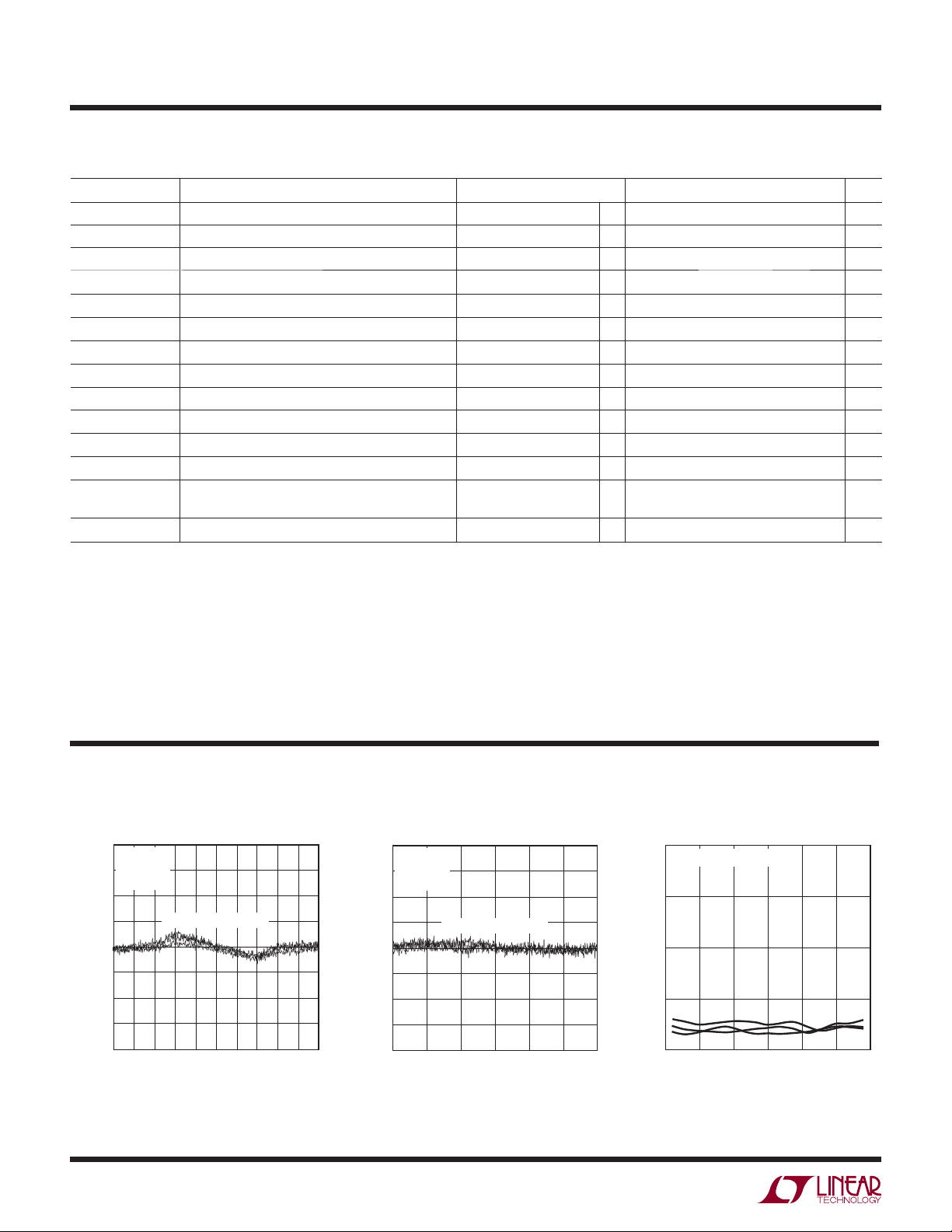
TYPICAL PERFORMANCE CHARACTERISTICS
Integral Nonlinearity, VCC = 5V
2.0
VCC = 5V
+
= 5V
V
1.5
REF
–
= 0V
V
REF
1.0
0.5
0
INL (LSB)
–0.5
–1.0
–1.5
–2.0
–5
TA = –45°C, 25°C, 90°C
–3 –1 1 52–4 –2 0 4
DIFFERENTIAL INPUT VOLTAGE (V)
3
2453 G01
Integral Nonlinearity, VCC = 3V Maximum INL vs Temperature
2.0
VCC = 3V
+
= 3V
V
REF
1.5
1.0
INL (LSB)
–0.5
–1.0
–1.5
–2.0
–
= 0V
V
REF
0.5
0
–3
TA = –45°C, 25°C, 90°C
–2 –1 1
DIFFERENTIAL INPUT VOLTAGE (V)
0
4
(TA = 25°C, unless otherwise noted)
VCC = V
1.5
1.0
INL (LSB)
0.5
0
3
2
2453 G02
–50
+
= 5V, 4.1V, 3V
REF
–25 0 25 50
TEMPERATURE (°C)
75 100
2453 G03
2453fa
Page 5
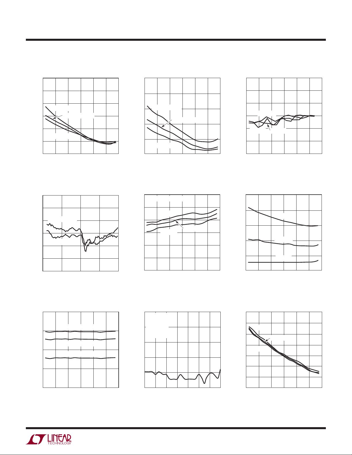
LTC2453
8
TYPICAL PERFORMANCE CHARACTERISTICS
Offset Error vs Temperature Gain Error vs Temperature Transition Noise vs Temperature
5
4
3
VCC = V
2
1
OFFSET ERROR (LSB)
VCC = V
0
–1
–50
+
= 3V
REF
VCC = V
+
= 5V
REF
02550
–25
TEMPERATURE (°C)
REF
+
= 4.1V
Transition Noise vs Output Code
3.0
2.5
REF
REF
+
= 3V
+
= 5V
VCC = V
2.0
1.5
VCC = V
1.0
TRANSITION NOISE RMS (μV)
0.5
75 100
2453 G04
5
4
VCC = V
3
2
GAIN ERROR (LSB)
1
VCC = V
0
–50
+
= 3V
REF
VCC = V
+
= 5V
REF
02550
–25
TEMPERATURE (°C)
REF
+
= 4.1V
Conversion Mode Power Supply
Current vs Temperature
1200
60Hz OUTPUT SAMPLE RATE
1000
VCC = 5V
800
600
400
CONVERSION CURRENT (μA)
200
VCC = 3V
VCC = 4.1V
(TA = 25°C, unless otherwise noted)
3.0
2.5
2.0
VCC = 4.1V
VCC = 5V VCC = 3V
0
–50
–25
02550
TEMPERATURE (°C)
75 100
2453 G05
1.5
1.0
TRANSITION NOISE RMS (μV)
0.5
Sleep Mode Power Supply
Current vs Temperature
250
200
150
100
SLEEP CURRENT (nA)
50
VCC = 5V
VCC = 4.1V
VCC = 3V
75 100
2453 G06
0
–32768 3276
–16384 163840
OUTPUT CODE
Average Power Dissipation vs
Temperature, V
10000
1000
100
10
AVERAGE POWER DISSIPATION (μW)
1
–50
25Hz OUTPUT SAMPLE RATE
10Hz OUTPUT SAMPLE RATE
1Hz OUTPUT SAMPLE RATE
–25 0 25 50
= 3V
CC
TEMPERATURE (°C)
75 100
2453 G07
2453 G10
0
–50
02550
–25
TEMPERATURE (°C)
Power Supply Rejection vs
Frequency at V
0
VCC = 4.1V
+
= 2.7V
V
REF
–
= 0V
V
REF
–20
+
= 1V
V
IN
–
= 2V
V
IN
–40
–60
REJECTIOIN (dB)
–80
–100
110
CC
1k
100
FREQUENCY AT VCC (Hz)
10k
100k
75 100
2453 G08
10M
1M
2453 G11
0
–50
02550
–25
TEMPERATURE (°C)
Conversion Time vs Temperature
21
20
VCC = 3V
19
18
VCC = 5V
17
16
CONVERSION TIME (ms)
15
14
–50
–25 0
TEMPERATURE (°C)
VCC = 4.1V
25 75
75 100
2453 G09
50 100
2453 G12
2453fa
5
Page 6

LTC2453
PIN FUNCTIONS
GND (Pin 1): Ground. Connect to a ground plane through
a low impedance connection.
–
(Pin 2), REF+ (Pin 3): Differential Reference Input.
REF
The voltage on these pins can have any value between
GND and V
as long as the reference positive input, REF+,
CC
remains more positive than the negative reference input,
–
, by at least 2.5V. The differential reference voltage
REF
= REF+ to REF–) sets the full-scale range.
(V
REF
(Pin 4): Positive Supply Voltage. Bypass to GND
V
CC
(Pin 1) with a 10μF capacitor in parallel with a low-series-inductance 0.1μF capacitor located as close to the
part as possible.
–
(Pin 5), IN+ (Pin 6): Differential Analog Input.
IN
BLOCK DIAGRAM
3 4
+
REF
SCL (Pin 7): Serial Clock Input of the I2C Interface. The
LTC2453 can only act as a slave and the SCL pin only accepts external serial clock. Data is shifted into the SDA pin
on the rising edges of SCL and output through the SDA
pin on the falling edges of SCL.
2
SDA (Pin 8): Bidirectional Serial Data Line of the I
C
Interface. The conversion result is output through the
SDA pin. The pin is high impedance unless the LTC2453
is in the data output mode. While the LTC2453 is in the
data output mode, SDA is an open drain pull down (which
requires an external 1.7k pull-up resistor to V
CC
).
Exposed Pad (Pin 9, DFN Only): Ground. Must be soldered
to PCB ground.
V
CC
+
IN
6
–
IN
5
16-BIT Δ∑
A/D CONVERTER
16-BIT Δ∑
A/D CONVERTER
REF
I2C
INTERFACE
DECIMATING
–
SINC FILTER
INTERNAL
OSCILLATOR
–
GND
12
SCL
SDA
7
8
2453 BD
6
2453fa
Page 7

APPLICATIONS INFORMATION
LTC2453
CONVERTER OPERATION
Converter Operation Cycle
The LTC2453 is a low-power, fully differential, delta-sigma
2
analog-to-digital converter with an I
C interface. Its operation, as shown in Figure 1, is composed of three successive
states: CONVERSION, SLEEP and DATA OUTPUT.
Initially, at power up, the LTC2453 performs a conversion.
Once the conversion is complete, the device enters the
sleep state. While in this sleep state, power consumption is
reduced by several orders of magnitude. The part remains
in the sleep state as long as it is not addressed for a read
operation. The conversion result is held indefi nitely in a
static shift register while the part is in the sleep state.
POWER-ON RESET
CONVERSION
SLEEP
edges of SCL, allowing the user to reliably latch data on
the rising edge of SCL. A new conversion is initiated by
a stop condition following a valid read operation, or by
the conclusion of a complete read cycle (all 16 bits read
out of the device).
Power-Up Sequence
When the power supply voltage (V
) applied to the con-
CC
verter is below approximately 2.1V, the ADC performs a
power-on reset. This feature guarantees the integrity of
the conversion result.
When VCC rises above this threshold, the converter
generates an internal power-on reset (POR) signal for
approximately 0.5ms. The POR signal clears all internal
registers. Following the POR signal, the LTC2453 starts
a conversion cycle and follows the succession of states
described in Figure 1. The fi rst conversion result following POR is accurate within the specifi cations of the
device if the power supply voltage VCC is restored within
the operating range (2.7V to 5.5V) before the end of the
POR time interval.
NO
NO
2453 F01
Figure 1. LTC2453 State Diagram
READ
ACKNOWLEDGE
YES
DATA OUTPUT
STOP
OR READ
16-BITS
YES
The device will not acknowledge an external request during
the conversion state. After a conversion is fi nished, the
device is ready to accept a read request. The LTC2453’s
address is hard-wired at 0010100. Once the LTC2453 is
addressed for a read operation, the device begins outputting the conversion result under the control of the serial
clock (SCL). There is no latency in the conversion result.
The data output is 16 bits long and contains a 15-bit plus
sign conversion result. Data is updated on the falling
Ease of Use
The LTC2453 data output has no latency, fi lter settling delay
or redundant results associated with the conversion cycle.
There is a one-to-one correspondence between the conversion and the output data. Therefore, multiplexing multiple
analog input voltages requires no special actions.
The LTC2453 performs offset calibrations every conversion. This calibration is transparent to the user and has
no effect upon the cyclic operation described previously. The advantage of continuous calibration is extreme
stability of the ADC performance with respect to time and
temperature.
The LTC2453 includes a proprietary input sampling scheme
that reduces the average input current by several orders
of magnitude when compared to traditional delta-sigma
architectures. This allows external fi lter networks to interface directly to the LTC2453. Since the average input
sampling current is 50nA, an external RC lowpass fi lter
using a 1kΩ and 0.1μF results in <1LSB additional error.
Additionally, there is negligible leakage current between
+
and IN–.
IN
2453fa
7
Page 8

LTC2453
APPLICATIONS INFORMATION
Reference Voltage Range
This converter accepts a truly differential external reference
voltage. The absolute/common mode voltage range for
+
and REF– pins covers the entire operating range of
REF
the device (GND to V
+
must be >(2.5V + V
V
REF
). For correct converter operation,
CC
REF
–
).
The LTC2453 differential reference input range is 2.5V to
. For the simplest operation, REF+ can be shorted to
V
CC
and REF– can be shorted to GND.
V
CC
Input Voltage Range
For most applications, V
REF
–
≤ (V
IN
+
, V
IN
–
) ≤ V
REF
+
. Under
these conditions the output code is given (see Data Format
section) as 32768 • (V
IN
– V
IN
–
)/(V
REF
+
– V
–
) + 32768.
REF
+
The output of the LTC2453 is clamped at a minimum value
of 0 and clamped at a maximum value of 65535.
The LTC2453 includes a proprietary system that can,
typically, correctly digitize each input 8LSB above
+
and below V
V
REF
–
, if the LTC2453’s output is not
REF
clamped. As an example (Figure 2), if the user desires to
measure a signal slightly below ground, the user could
–
IN
= V
set V
the output code would be approximately 32768. If V
–
= GND, and V
REF
REF
+
= 5V. If V
+
= GND,
IN
IN
+
= GND – 8LSB = –1.22 mV, the output code would be
approximately 32760.
I2C INTERFACE
2
The LTC2453 communicates through an I
2
C interface is a 2-wire open-drain interface supporting
I
C interface. The
multiple devices and masters on a single bus. The connected devices can only pull the data line (SDA) LOW and
never drive it HIGH. SDA must be externally connected to
the supply through a pull-up resistor. When the data line
2
is free, it is HIGH. Data on the I
C bus can be transferred
at rates up to 100kbits/s in the Standard-Mode and up to
400kbits/s in the Fast-Mode.
2
Each device on the I
C bus is recognized by a unique
address stored in that device and can operate either as
a transmitter or receiver, depending on the function of
the device. In addition to transmitters and receivers,
devices can also be considered as masters or slaves when
performing data transfers. A master is the device which
initiates a data transfer on the bus and generates the
clock signals to permit that transfer. Devices addressed
by the master are considered a slave. The address of the
LTC2453 is 0010100.
The LTC2453 can only be addressed as a slave. It can only
transmit the last conversion result. The serial clock line,
SCL, is always an input to the LTC2453 and the serial data
line SDA is bidirectional. Figure 3 shows the defi nition of
2
C timing.
the I
32788
32784
32780
32776
32772
32768
32764
OUTPUT CODE
32760
32756
32752
32748
–0.001
Figure 2. Output Code vs V
8
–0.005
SIGNALS
BELOW
GND
0
V
IN
+
IN
0.005
+
+
/V
REF
with V
0.001
–
= 0 and V
IN
0.0015
2453 F02
REF
–
= 0
The START and STOP Conditions
A START (S) condition is generated by transitioning SDA
from HIGH to LOW while SCL is HIGH. The bus is considered to be busy after the START condition. When the data
transfer is fi nished, a STOP (P) condition is generated by
transitioning SDA from LOW to HIGH while SCL is HIGH.
The bus is free after a STOP is generated. START and STOP
conditions are always generated by the master.
When the bus is in use, it stays busy if a repeated START
(Sr) is generated instead of a STOP condition. The repeated
START timing is functionally identical to the START and
is used for reading from the device before the initiation
of a new conversion.
2453fa
Page 9

APPLICATIONS INFORMATION
SDA
t
r
t
HD(DAT)
SU(DAT)
t
HIGH
t
SCL
t
f
t
LOW
t
HD(STA)
SSrPS
Figure 3. Defi nition of Timing for Fast/Standard Mode Devices on the I2C Bus
LTC2453
t
t
f
t
SU(STA)
t
HD(SDA)
t
SP
t
SU(STO)
r
t
BUF
Data Transferring
After the START condition, the I2C bus is busy and data
transfer can begin between the master and the addressed
slave. Data is transferred over the bus in groups of nine
bits, one byte followed by one acknowledge (ACK) bit. The
master releases the SDA line during the ninth SCL clock
cycle. The slave device can issue an ACK by pulling SDA
LOW or issue a Not Acknowledge (NAK) by leaving the
SDA line HIGH impedance (the external pull-up resistor
will hold the line HIGH). Change of data only occurs while
the clock line (SCL) is LOW.
Data Format
After a START condition, the master sends a 7-bit address
followed by a read request (R) bit. The bit R is 1 for a
Read Request. If the 7-bit address matches the LTC2453’s
address (hard-wired at 0010100) the ADC is selected. When
the device is addressed during the conversion state, it does
not accept the request and issues a NAK by leaving the
SDA line HIGH. If the conversion is complete, the LTC2453
issues an ACK by pulling the SDA line LOW.
Following the ACK, the LTC2453 can output data. The data
output stream is 16 bits long and is shifted out on the
falling edges of SCL (see Figure 4). The fi rst bit output by
+
the LTC2453, the MSB, is the sign, which is 1 for V
–
and 0 for V
V
IN
IN
+
< V
–
(see Table 1). The MSB (D15) is
IN
IN
≥
followed by successively less signifi cant bits (D14, D13…)
until the LSB is output by the LTC2453. This sequence is
shown in Figure 5.
OPERATION SEQUENCE
Continuous Read
Conversions from the LTC2453 can be continuously
read, see Figure 6. At the end of a read operation, a new
conversion automatically begins. At the conclusion of
the conversion cycle, the next result may be read using
the method described above. If the conversion cycle is
not complete and a valid address selects the device, the
LTC2453 generates a NAK signal indicating the conversion
cycle is in progress.
Discarding a Conversion Result and Initiating a New
Conversion
It is possible to start a new conversion without reading
the old result, as shown in Figure 7. Following a valid 7-bit
address, a read request (R) bit, and a valid ACK, a STOP
command will start a new conversion.
PRESERVING THE CONVERTER ACCURACY
The LTC2453 is designed to dramatically reduce the conversion result’s sensitivity to device decoupling, PCB layout,
antialiasing circuits, line and frequency perturbations. Nevertheless, in order to preserve the high accuracy capability
of this part, some simple precautions are desirable.
Digital Signal Levels
Due to the nature of CMOS logic, it is advisable to keep
input digital signals near GND or V
range of 0.5V to V
– 0.5V may result in additional cur-
CC
. Voltages in the
CC
2453fa
9
Page 10

LTC2453
V
APPLICATIONS INFORMATION
SCL
1789 2318
7-BIT
ADDRESS
START BY
MASTER
SLEEP DATA OUTPUT CON
ACK BY
LTC2453
D15RSDA
(SGN)
MSB
9123 89
D8D13D14
MASTER
D7 D6 D5 D0
ACK BY
Figure 4. Read Sequence Timing Diagram
Table 1. LTC2453 Output Data Format. FS = V
DIFFERENTIAL INPUT
VOLTAGE V
+
- V
IN
IN
D15
-
(MSB) D14 D13 D12 ... D2 D1D0(LSB)
REF
+
≥FS 1 1 1 1 1 1 65535
FS - 1LSB 1 1 1 1 1 0 65534
0.5 • FS 1 1 0 0 0 0 49152
0.5 • FS - 1LSB 1 0 1 1 1 1 49151
0 1 0 0 0 0 0 32768
-1LSB 0 1 1 1 1 1 32767
-0.5 • FS 0 1 0 0 0 0 16384
-0.5 • FS - 1LSB 0 0 1 1 1 1 16383
≤-FS 0 0 0 0 0 0 0
– V
REF
-
.
CORRESPONDING
DECIMAL VALUE
LSB
NACK BY
MASTER
7-BIT ADDRESS
SPR ACK READ
(0010100)
SLEEP
DATA OUTPUT CONVERSIONCONVERSION
2453 F05
Figure 5. The LTC2453 Coversion Sequence
7-BIT ADDRESS
SPR ACK READ READ
(0010100)
CONVERSION CONVERSION
SLEEP SLEEP
CONVERSIONDATA OUTPUT
7-BIT ADDRESS
S RPACK
(0010100)
DATA OUTPUT
2453 F06
Figure 6. Consecutive Reading at the Same Confi guration
7-BIT ADDRESS
SPR ACK READ (OPTIONAL)
(0010100)
SLEEP
DATA OUTPUT CONVERSIONCONVERSION
2453 F07
Figure 7. Start a New Conversion without Reading Old Conversion Result
2453fa
10
Page 11

APPLICATIONS INFORMATION
LTC2453
rent leakage from the part.
Driving V
In relation to the V
and GND
CC
and GND pins, the LTC2453 combines
CC
internal high frequency decoupling with damping elements,
which reduce the ADC performance sensitivity to PCB
layout and external components. Nevertheless, the very
high accuracy of this converter is best preserved by careful
low and high frequency power supply decoupling.
A 0.1μF, high quality, ceramic capacitor in parallel with a
10μF ceramic capacitor should be connected between the
and GND pins, as close as possible to the package.
V
CC
The 0.1μF capacitor should be placed closest to the ADC
package. It is also desirable to avoid any via in the circuit
path, starting from the converter V
pin, passing through
CC
these two decoupling capacitors, and returning to the
converter GND pin. The area encompassed by this circuit
path, as well as the path length, should be minimized.
Very low impedance ground and power planes, and star
connections at both V
I
LEAK
+
REF
I
LEAK
I
LEAK
+
IN
I
LEAK
I
LEAK
–
IN
I
LEAK
I
LEAK
–
REF
I
LEAK
and GND pins, are preferable.
CC
V
CC
R
SW
15k
(TYP)
V
CC
R
SW
15k
(TYP)
C
2453 F08
EQ
0.35pF
(TYP)
V
CC
R
SW
15k
(TYP)
V
CC
R
SW
15k
(TYP)
The VCC pin should have three distinct connections: the
fi rst to the decoupling capacitors described above, the
second to the ground return for the input signal source,
and the third to the ground return for the power supply
voltage source.
Driving REF
+
and REF
–
A simplifi ed equivalent circuit for REF+ and REF– is shown
in Figure 8. Like all other A/D converters, the LTC2453 is
only as accurate as the reference it is using. Therefore,
it is important to keep the reference line quiet by careful
low and high frequency power supply decoupling.
The LT6660 reference is an ideal match for driving the
+
LTC2453’s REF
pin. The LTC6660 is available in a 2mm ×
2mm DFN package with 2.5V, 3V, 3.3V and 5V options.
A 0.1μF, high quality, ceramic capacitor in parallel with
a 10μF ceramic capacitor should be connected between
+
the REF
/REF– and GND pins, as close as possible to the
package. The 0.1μF capacitor should be placed closest
to the ADC.
Driving V
IN
+
and V
IN
–
The input drive requirements can best be analyzed using
the equivalent circuit of Figure 9. The input signal V
+
connected to the ADC input pins (IN
an equivalent source resistance R
and IN–) through
. This resistor includes
S
SIG
is
both the actual generator source resistance and any additional optional resistors connected to the input pins.
V
CC
R
SW
15k
(TYP)
C
EQ
0.35pF
(TYP)
V
CC
R
SW
15k
(TYP)
C
EQ
0.35pF
(TYP)
I
CONV
I
CONV
2453 F09
SIG
SIG
I
R
S
+
+
–
–
+
–
C
IN
R
S
C
IN
LEAK
+
IN
I
LEAK
C
PAR
I
LEAK
–
IN
I
LEAK
C
PAR
Figure 8. LTC2453 Analog Input/Reference Equivalent Circuit
Figure 9. LTC2453 Input Drive Equivalent Circuit
2453fa
11
Page 12

LTC2453
APPLICATIONS INFORMATION
Optional input capacitors CIN are also connected to the
ADC input pins. This capacitor is placed in parallel with the
ADC input parasitic capacitance C
PCB layout, C
has typical values between 2pF and 15pF.
PAR
. Depending on the
PAR
In addition, the equivalent circuit of Figure 9 includes the
converter equivalent internal resistor R
capacitor C
EQ
.
There are some immediate trade-offs in R
needing a full circuit analysis. Increasing R
and sampling
SW
and CIN without
S
and CIN can
S
give the following benefi ts:
1) Due to the LTC2453’s input sampling algorithm, the
input current drawn by either V
IN
version cycle is 50nA. A high R
+
or V
• CIN attenuates the
S
–
over a con-
IN
high frequency components of the input current, and
values up to 1k result in <1LSB error.
R
S
2) The bandwidth from V
+
, IN–). This bandwidth reduction isolates the ADC
(IN
is reduced at the input pins
SIG
from high frequency signals, and as such provides
simple antialiasing and input noise reduction.
3) Switching transients generated by the ADC are attenuated before they go back to the signal source.
4) A large C
gives a better AC ground at the input pins,
IN
helping reduce refl ections back to the signal source.
5) Increasing R
protects the ADC by limiting the current
S
during an outside-the-rails fault condition.
There is a limit to how large R
• CIN should be for a given
S
application. Increasing RS beyond a given point increases
the voltage drop across R
due to the input current,
S
to the point that signifi cant measurement errors exist.
Additionally, for some applications, increasing the R
• C
S
IN
product too much may unacceptably attenuate the signal
at frequencies of interest.
For most applications, it is desirable to implement C
a high-quality 0.1μF ceramic capacitor and R
≤ 1k. This
S
IN
as
capacitor should be located as close as possible to the
actual V
package pin. Furthermore, the area encompassed
IN
by this circuit path, as well as the path length, should be
minimized.
In the case of a 2-wire sensor that is not remotely
grounded, it is desirable to split R
and place series
S
resistors in the ADC input line as well as in the sensor
ground return line, which should be tied to the ADC GND
pin using a star connection topology.
Figure 10 shows the measured LTC2453 INL vs Input
Voltage as a function of R
= 0.1μF.
C
IN
In some cases, R
can be increased above these guidelines.
S
value with an input capacitor
S
The input current is zero when the ADC is either in sleep
or I/O modes. Thus, if the time constant of the input RC
circuit τ = R
• CIN, is of the same order of magnitude or
S
longer than the time periods between actual conversions,
then one can consider the input current to be reduced
correspondingly.
12
10
CIN = 0.1μF
8
= 5V
V
CC
= 25°C
T
A
6
RS = 2k
–3–4
RS = 10k
RS = 0
–1–2
12 4
0
3
5
2453 F10
4
2
0
INL (LSB)
–2
–4
–6
–8
–10
–5
RS = 1k
DIFFERENTIAL INPUT VOLTAGE (V)
Figure 10. Measured INL vs Input Voltage,
CIN = 0.1μF, VCC = 5V, TA = 25°C
10
CIN = 0
8
= 5V
V
CC
= 25°C
T
A
6
4
RS = 10k
2
0
INL (LSB)
–2
–4
–6
–8
–10
RS = 0
RS = 1k, 2k
–3–4
–5
DIFFERENTIAL INPUT VOLTAGE (V)
–1–2
0
12 4
3
2453 F11
5
Figure 11. Measured INL vs Input Voltage,
CIN = 0, VCC = 5V, TA = 25°C
2453fa
Page 13

APPLICATIONS INFORMATION
LTC2453
0
–20
–40
–60
–80
INPUT SIGNAL ATTENUATION (dB)
–100
0
Figure 12. LTC2453 Input Signal Attentuation vs Frequency Figure 13. LTC2453 Input Signal Attenuation
5.0 7.5
2.5
INPUT SIGNAL FREQUENCY (MHz)
These considerations need to be balanced out by the input
signal bandwidth. The 3dB bandwidth ≈ 1/(2πR
Finally, if the recommended choice for C
for the user’s specifi c application, an alternate strategy is to
eliminate C
and minimize C
IN
PAR
this confi guration corresponds to a low impedance sensor
directly connected to the ADC through minimum length
traces. Actual applications include current measurements
through low value sense resistors, temperature measurements, low impedance voltage source monitoring, and so
on. The resultant INL vs V
IN
measurements of Figure 11 include a capacitor C
responding to a minimum sized layout pad and a minimum
width input trace of about 1 inch length.
1.00 1.25 1.50
2453 F12
).
SCIN
is unacceptable
IN
and RS. In practical terms,
is shown in Figure 11. The
cor-
PAR
On a related note, the LTC2453 uses two separate A/D
converters to digitize the positive and negative inputs.
Each of these A/D converters has 1.4μV
noise. If one of the input voltages is within this small
transition noise band, then the output will fl uctuate one
bit, regardless of the value of the other input voltage. If
both of the input voltages are within their transition noise
bands, the output can fl uctuate 2 bits.
For a simple system noise analysis, the V
be modeled as a single-pole equivalent circuit characterized by a pole location f
If the converter has an unlimited bandwidth, or at least a
bandwidth substantially larger than f
contribution of the external drive circuit would be:
0
–5
–10
–15
–20
–25
–30
–35
–40
INPUT SIGNAL ATTENUATIOIN (dB)
–45
–50
vs Frequency (Low Frequencies)
12060
0
240180
300
INPUT SIGNAL FREQUENCY (Hz)
and a noise spectral density ni.
i
360 420 540
480
drive circuit can
IN
, then the total noise
i
600
2453 F13
transition
RMS
Signal Bandwidth, Transition Noise and Noise
Equivalent Input Bandwidth
1
The LTC2453 includes a sinc
notch located at f
= 60Hz. As such, the 3dB input signal
0
type digital fi lter with the fi rst
bandwidth is 26.54Hz. The calculated LTC2453 input signal
attenuation vs frequency over a wide frequency range is
shown in Figure 12. The calculated LTC2453 input signal
attenuation vs frequency at low frequencies is shown in
Figure 13. The converter noise level is about 1.4μV
RMS
and can be modeled by a white noise source connected
at the input of a noise-free converter.
Vn f
=π/•2
ni i
Then, the total system noise level can be estimated as
2
the square root of the sum of (V
LTC2453 noise fl oor (~1.4μV
) and the square of the
n
2
).
2453fa
13
Page 14

LTC2453
TYPICAL APPLICATION
+
E5
REF
E1
IN
E2
IN
E3
V
E4
GND
E6
REF
V
+
R1
+
1k
R9
–
1k
0.1μF
CC
V
CC
–
C4
1μF
C6
3
IN
GND GND
C2
0.1μF
LT6660
OUT
42
C7
0.1μF
6
5
5V
C3
1μF
R4
1.0Ω
0.1μF
IN
IN
0.1μF
JP1
C1
REF
+
–
REF
C8
EXT
V
CC
34
+
V
CC
LTC2453
–
GND
21
1
C10
0.1μF
EXT
SCL
SDA
GND
JP2
GND
DC1266A Demo Board Schematic
SCL SDA
7
R7
R6
4.99k
8
9
4.99k
1%
1%
6
7
3
2
1
V
CC
SCL
WP
24LC025-I/ST
A2
A1
A0
GND
+
V
CC
C9
1μF
8
4
SDA
R8
4.99k
1%
C5
0.1μF
5
V
1
2
6
4
7
5
11
10
9
12
14
VUNREG
5V
CS
SCK/SCL
MOSI/SDA
MISO
J1
EESCL
EEVCC
EESDA
EEGND
NC
GND GND
GND
3
2453 TA02
TO
CONTROLLER
813
PACKAGE DESCRIPTION
DDB Package
8-Lead Plastic DFN (3mm × 2mm)
(Reference LTC DWG # 05-08-1702 Rev B)
0.61 ±0.05
(2 SIDES)
0.70 ±0.05
2.55 ±0.05
1.15 ±0.05
PACKAGE
OUTLINE
0.25 ± 0.05
0.50 BSC
2.20 ±0.05
(2 SIDES)
RECOMMENDED SOLDER PAD PITCH AND DIMENSIONS
NOTE:
1. DRAWING CONFORMS TO VERSION (WECD-1) IN JEDEC PACKAGE OUTLINE M0-229
2. DRAWING NOT TO SCALE
3. ALL DIMENSIONS ARE IN MILLIMETERS
4. DIMENSIONS OF EXPOSED PAD ON BOTTOM OF PACKAGE DO NOT INCLUDE
MOLD FLASH. MOLD FLASH, IF PRESENT, SHALL NOT EXCEED 0.15mm ON ANY SIDE
5. EXPOSED PAD SHALL BE SOLDER PLATED
6. SHADED AREA IS ONLY A REFERENCE FOR PIN 1 LOCATION ON THE TOP AND BOTTOM OF PACKAGE
PIN 1 BAR
TOP MARK
(SEE NOTE 6)
0.200 REF
3.00 ±0.10
(2 SIDES)
2.00 ±0.10
(2 SIDES)
0.75 ±0.05
R = 0.05
0 – 0.05
R = 0.115
TYP
TYP
0.56 ± 0.05
(2 SIDES)
0.25 ± 0.05
BOTTOM VIEW—EXPOSED PAD
2.15 ±0.05
(2 SIDES)
0.40 ± 0.10
85
14
0.50 BSC
PIN 1
R = 0.20 OR
0.25 × 45°
CHAMFER
(DDB8) DFN 0905 REV B
2453fa
14
Page 15

PACKAGE DESCRIPTION
LTC2453
TSOT Package
8-Lead Plastic TSOT
(Reference LTC TS8 # 05-08-1637)
0.52
MAX
3.85 MAX
2.62 REF
RECOMMENDED SOLDER PAD LAYOUT
PER IPC CALCULATOR
0.20 BSC
DATUM ‘A’
0.30 – 0.50 REF
NOTE:
1. DIMENSIONS ARE IN MILLIMETERS
2. DRAWING NOT TO SCALE
3. DIMENSIONS ARE INCLUSIVE OF PLATING
4. DIMENSIONS ARE EXCLUSIVE OF MOLD FLASH AND METAL BURR
5. MOLD FLASH SHALL NOT EXCEED 0.254mm
6. JEDEC PACKAGE REFERENCE IS MO-193
0.65
REF
1.22 REF
1.4 MIN
2.80 BSC
0.09 – 0.20
(NOTE 3)
1.50 – 1.75
(NOTE 4)
1.00 MAX
0.65 BSC
0.80 – 0.90
2.90 BSC
(NOTE 4)
PIN ONE ID
0.22 – 0.36
8 PLCS (NOTE 3)
0.01 – 0.10
1.95 BSC
TS8 TSOT-23 0802
Information furnished by Linear Technology Corporation is believed to be accurate and reliable.
However, no responsibility is assumed for its use. Linear Technology Corporation makes no representation that the interconnection of its circuits as described herein will not infringe on existing patent rights.
2453fa
15
Page 16

LTC2453
RELATED PARTS
PART NUMBER DESCRIPTION COMMENTS
LT1236A-5 Precision Bandgap Reference, 5V 0.05% Max, 5ppm/°C Drift
LT1461 Micropower Series Reference, 2.5V 0.04% Max, 3ppm/°C Drift
LT1790 Micropower Precision Reference in TSOT-23-6 Package 60μA Max Supply Current, 10ppm/°C Max Drift, 1.25V, 2.048V,
LTC1860/LTC1861 12-Bit, 5V, 1-/2-Channel 250ksps SAR ADC in MSOP 850μA at 250ksps, 2μA at 1ksps, SO-8 and MSOP Packages
LTC1860L/LTC1861L 12-Bit, 3V, 1-/2-Channel 150ksps SAR ADC 450μA at 150ksps, 10μA at 1ksps, SO-8 and MSOP Packages
LTC1864/LTC1865 16-Bit, 5V, 1-/2-Channel 250ksps SAR ADC in MSOP 850μA at 250ksps, 2μA at 1ksps, SO-8 and MSOP Packages
LTC1864L/LTC1865L 16-bit, 3V, 1-/2-Channel 150ksps SAR ADC 450μA at 150ksps, 10μA at 1ksps, SO-8 and MSOP Packages
LTC2440
LTC2480
LTC2481
LTC2482
LTC2483
LTC2484
LTC2485
LTC6241 Dual, 18MHz, Low Noise, Rail-to-Rail Op Amp 550nV
LT6660
LTC2450 Easy-to-Use, Ultra-Tiny 16-Bit ADC
LTC2450-1 Easy-to-Use, Ultra-Tiny 16-Bit ADC
No Latency ΔΣ is a trademark of Linear Technology Corporation.
24-Bit No Latency ΔΣ
16-Bit, Differential Input, No Latency ΔΣ ADC, with PGA,
Temp. Sensor, SPI
16-Bit, Differential Input, No Latency ΔΣ ADC, with PGA,
Temp. Sensor, I
16-Bit, Differential Input, No Latency ΔΣ ADC, SPI
16-Bit, Differential Input, No Latency ΔΣ ADC, I
24-Bit, Differential Input, No Latency ΔΣ ADC, SPI
24-Bit, Differential Input, No Latency ΔΣ ADC, I
Micropower References in 2mm × 2mm DFN Package,
2.5V, 3V, 3.3V, 5V
TM
ADC
2
C
2
C
2
C
2.5V, 3V, 3.3V, 4.096V and 5V Options
200nV
Easy-Drive Input Current Cancellation, 600nV
Tiny 10-Lead DFN Package
Easy-Drive Input Current Cancellation, 600nV
Tiny 10-Lead DFN Package
Easy-Drive Input Current Cancellation, 600nV
Tiny 10-Lead DFN Package
Easy-Drive Input Current Cancellation, 600nV
Tiny 10-Lead DFN Package
Easy-Drive Input Current Cancellation, 600nV
Tiny 10-Lead DFN Package
Easy-Drive Input Current Cancellation, 600nV
Tiny 10-Lead DFN Package
20ppm/°C max drift, 0.2% Max
2 LSB INL, 50nA Sleep current, Tiny 2mm × 2mm DFN-6 Package,
30Hz Output Rate
2 LSB INL, 50nA Sleep Current, Tiny 2mm × 2mm DFN-6 Package,
60Hz Output Rate
Noise, 8kHz Output Rate, 15ppm INL
RMS
Noise, 125μV Offset Max
P-P
RMS
RMS
RMS
RMS
RMS
RMS
Noise,
Noise,
Noise,
Noise,
Noise,
Noise,
16
Linear Technology Corporation
1630 McCarthy Blvd., Milpitas, CA 95035-7417
(408) 432-1900 l FAX: (408) 434-0507
l
www.linear.com
2453fa
LT 0308 REV A • PRINTED IN USA
© LINEAR TECHNOLOGY CORPORATION 2007
 Loading...