

Page 1
FEATURES
LTC2433-1
Differential Input
16-Bit No Latency ∆Σ ADC
U
DESCRIPTIO
■
16-Bit Differential ADC in a Tiny MSOP
■
Low Supply Current: 200µA, 4µA in Autosleep
■
Rail-to-Rail Differential Input/Reference
■
0.12LSB INL, No Missing Codes
■
0.16LSB Full-Scale Error and 5µV Offset
■
1.45µV RMS Noise, Independent of V
■
Very Low Transition Noise: <0.02LSB
■
Operates with a Reference as Low as 100mV with
REF
16-Bit Resolution
■
Internal Oscillator—No External Components
Required
■
87dB Min, Simultaneous 50Hz and 60Hz Notch Filter
■
Single Supply 2.7V to 5.5V Operation
■
Pin Compatible with the 20/24-Bit LTC2431/LTC2411
■
Available in 10-Lead MSOP Package
U
APPLICATIO S
■
Direct Sensor Digitizer
■
Weight Scales
■
Direct Temperature Measurement
■
Gas Analyzers
■
Strain-Gage Transducers
■
Instrumentation
■
Data Acquisition
■
Industrial Process Control
The LTC®2433-1 is a differential input micropower 16-bit
No Latency ∆ΣTM analog-to-digital converter with an integrated oscillator. It provides 0.12LSB INL and 1.45µV
RMS noise independent of V
. It uses delta-sigma
REF
technology and provides single conversion settling of the
digital filter. Through a single pin, the LTC2433-1 can be
configured for better than 87dB input differential mode
rejection at 50Hz and 60Hz ±2%, or it can be driven by an
external oscillator for a user defined rejection frequency.
The internal oscillator requires no external frequency
setting components.
The converter accepts any external differential reference
voltage from 0.1V to VCC for flexible ratiometric and
remote sensing measurement configurations. The fullscale differential input range is from –0.5 •␣ V
V
. The reference common mode voltage, V
REF
the input common mode voltage, V
, may be indepen-
INCM
to 0.5 •
REF
REFCM
, and
dently set anywhere between GND and VCC. The DC
common mode input rejection is better than 140dB.
The LTC2433-1 communicates through a flexible 3-wire
digital interface which is compatible with SPI and
MICROWIRETM protocols.
, LTC and LT are registered trademarks of Linear Technology Corporation.
No Latency ∆Σ is a trademark of Linear Technology Corporation.
MICROWIRE is a trademark of National Semiconductor Corporation.
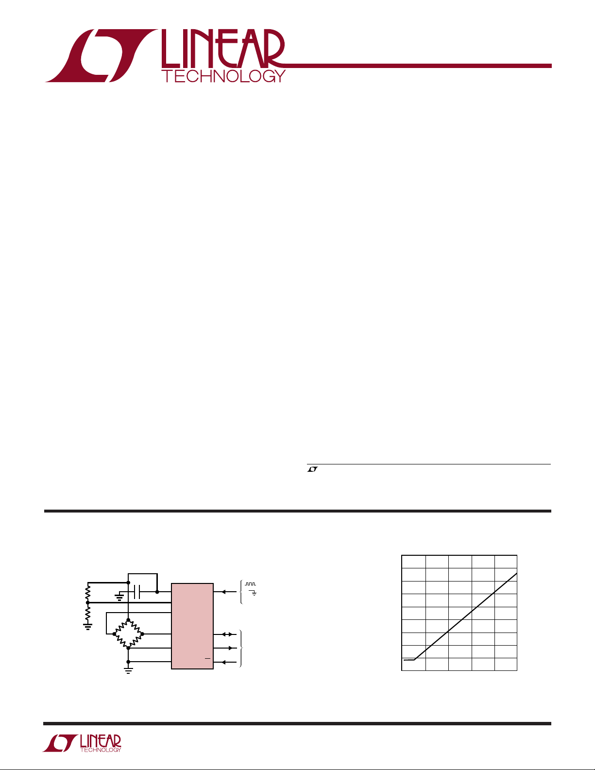
TYPICAL APPLICATIO
5V REF
4.9k
100Ω
1µF
(100mV)
110
V
CC
2
REF
4
+
IN
LTC2433-1
5
–
IN
3
REF
6
GND
U
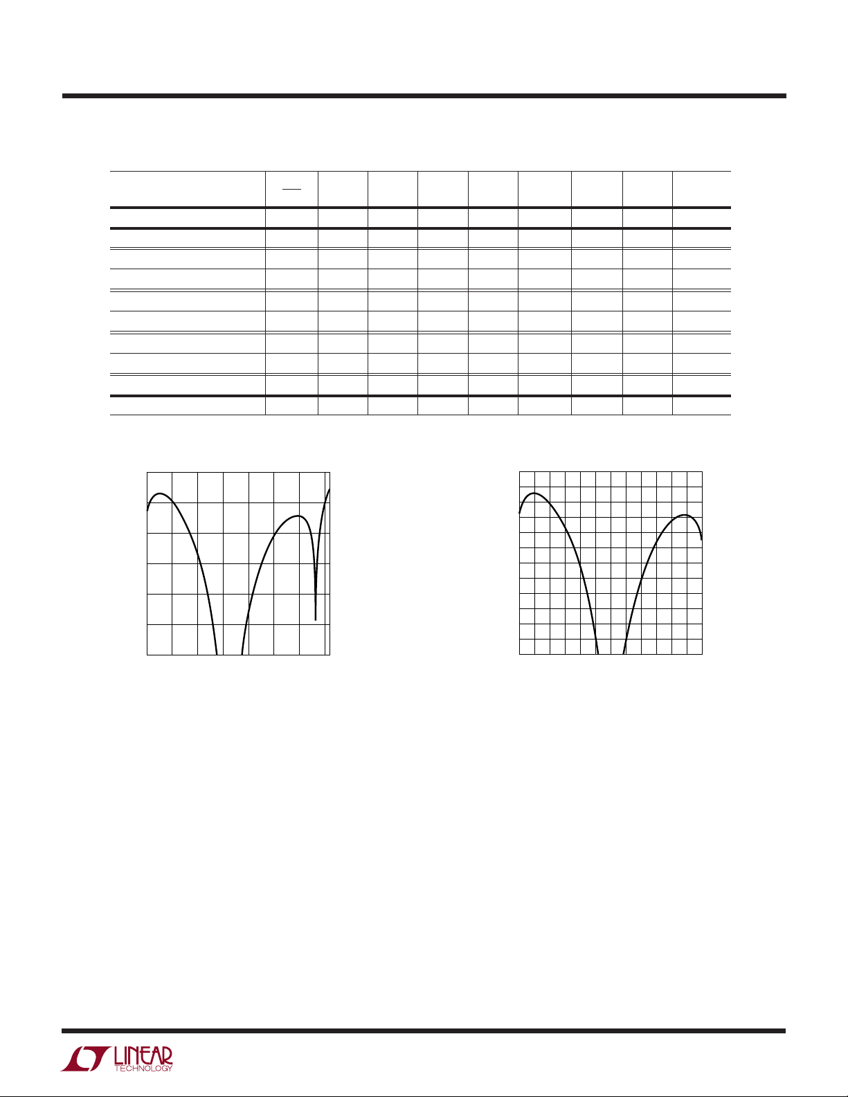
Minimum Resolvable Signal vs V
90
80
= EXTERNAL CLOCK SOURCE
F
O
+
9
SCK
SDO
8
7
CS
24331 TA01
–
= INTERNAL OSC/SIMULTANEOUS
50Hz/60Hz REJECTION
3-WIRE
SPI INTERFACE
70
60
50
40
30
20
10
MINIMUM RESOLVABLE SIGNAL (µV)*
0
0
13
*FOR V
REF
IS LIMITED BY STEP SIZE
2
V
(V)
REF
≥ 0.5V THE RESOLUTION
4
24331 TA02
REF
5
24331fa
1
Page 2
LTC2433-1
WWWU
ABSOLUTE AXI U RATI GS
PACKAGE/ORDER I FOR ATIO
UU
W
(Notes 1, 2)
Supply Voltage (VCC) to GND.......................–0.3V to 7V
ORDER PART NUMBER
Analog Input Voltage
to GND.................................... –0.3V to (VCC + 0.3V)
Reference Input Voltage
to GND.................................... –0.3V to (VCC + 0.3V)
Digital Input Voltage to GND........ –0.3V to (VCC + 0.3V)
Digital Output Voltage to GND ..... –0.3V to (VCC + 0.3V)
Operating Temperature Range
LTC2433-1C ............................................ 0°C to 70°C
LTC2433-1I ........................................ –40°C to 85°C
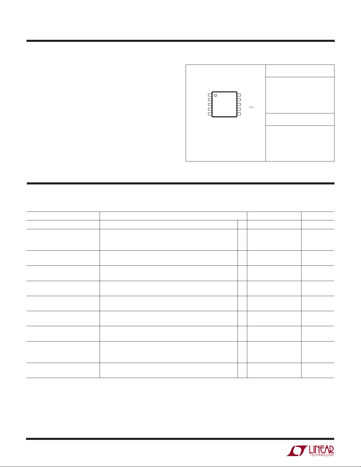
TOP VIEW
1
V
CC
+
2
REF
–
REF
3
+
IN
4
–
IN
5
MS10 PACKAGE
10-LEAD PLASTIC MSOP
T
= 125°C, θJA = 110°C/W
JMAX
10
F
O
SCK
9
SDO
8
CS
7
GND
6
LTC2433-1CMS
LTC2433-1IMS
MS PART MARKING
LTAEY
LTAEZ
Storage Temperature Range ................. –65°C to 150°C
Lead Temperature (Soldering, 10 sec)..................300°C
ELECTRICAL CHARACTERISTICS
temperature range, otherwise specifications are at TA = 25°C. (Notes 3, 4, 6)
PARAMETER CONDITIONS MIN TYP MAX UNITS
Resolution (No Missing Codes) 0.1V ≤ V
Integral Nonlinearity (Note 15) 5V ≤ VCC ≤ 5.5V, REF+ = 2.5V, REF– = GND, V
5V ≤ V
REF
Offset Error (Note 15) 2.5V ≤ REF+ ≤ VCC, REF– = GND, ● 520 µV
GND ≤ IN
Offset Error Drift 2.5V ≤ REF+ ≤ VCC, REF– = GND, 20 nV/°C
GND ≤ IN
Positive Full-Scale Error (Note 15) 2.5V ≤ REF+ ≤ VCC, REF– = GND, ● 0.16 1.25 LSB
Positive Full-Scale Error Drift 2.5V ≤ REF+ ≤ VCC, REF– = GND, 0.04 ppm of V
Negative Full-Scale Error (Note 15) 2.5V ≤ REF+ ≤ VCC, REF– = GND, ● 0.16 1.25 LSB
Negative Full-Scale Error Drift 2.5V ≤ REF+ ≤ VCC, REF– = GND, 0.04 ppm of V
Total Unadjusted Error 5V ≤ VCC ≤ 5.5V, REF+ = 2.5V, REF– = GND, V
Output Noise 5V ≤ VCC ≤ 5.5V, REF+ = 5V, REF– = GND, 1.45 µV
+
IN
+
IN
+
IN
+
IN
5V ≤ V
REF
GND ≤ IN– = IN+ ≤ VCC, (Note 12)
≤ VCC, –0.5 • V
REF
≤ 5.5V, REF+ = 5V, REF– = GND, V
CC
+
= 2.5V, REF– = GND, V
+
= IN– ≤ VCC, (Note 13)
+
= IN– ≤ V
= 0.75REF+, IN– = 0.25 • REF
= 0.75REF+, IN– = 0.25 • REF
= 0.25 • REF+, IN– = 0.75 • REF
= 0.25 • REF+, IN– = 0.75 • REF
≤ 5.5V, REF+ = 5V, REF– = GND, V
CC
+
= 2.5V, REF– = GND, V
CC
The ● denotes specifications which apply over the full operating
≤ VIN ≤ 0.5 • V
REF
= 1.25V, (Note 6) 0.30 LSB
INCM
+
+
= 1.25V, (Note 6) 0.25 LSB
INCM
Consult LTC Marketing for parts specified with wider operating temperature ranges.
, (Note 5) ● 16 Bits
REF
= 1.25V, (Note 6) 0.06 LSB
INCM
= 2.5V, (Note 6) ● 0.12 1.25 LSB
INCM
+
+
= 1.25V 0.20 LSB
INCM
= 2.5V 0.20 LSB
INCM
REF
REF
/°C
/°C
RMS
2
24331fa
Page 3
LTC2433-1
U
CO VERTER CHARACTERISTICS
temperature range, otherwise specifications are at TA = 25°C. (Notes 3, 4)
PARAMETER CONDITIONS MIN TYP MAX UNITS
Input Common Mode Rejection DC 2.5V ≤ REF+ ≤ VCC, REF– = GND, ● 130 140 dB
GND ≤ IN
Input Common Mode Rejection 2.5V ≤ REF+ ≤ VCC, REF– = GND, ● 140 dB
49Hz to 61.2Hz GND ≤ IN
Input Normal Mode Rejection (Note 5, 7) ● 87 dB
49Hz to 61.2Hz
Reference Common Mode 2.5V ≤ REF+ ≤ VCC, GND ≤ REF– ≤ 2.5V, ● 130 140 dB
Rejection DC V
Power Supply Rejection, DC REF+ = 2.5V, REF– = GND, IN– = IN+ = GND 120 dB
Power Supply Rejection, REF+ = 2.5V, REF– = GND, IN– = IN+ = GND, (Note 7) 120 dB
Simultaneous 50Hz/60Hz ±2%
–
= IN+ ≤ V
–
= IN+ ≤ VCC, (Notes 5, 7)
= 2.5V, IN– = IN+ = GND (Note 5)
REF
CC
The ● denotes specifications which apply over the full operating
(Note 5)
UU
A ALOG I PUT A D REFERE CE
UU
The ● denotes specifications which apply over the full operating
temperature range, otherwise specifications are at TA = 25°C. (Note 3)
SYMBOL PARAMETER CONDITIONS MIN TYP MAX UNITS
+
IN
–
IN
V
IN
+
REF
–
REF
V
REF
CS (IN+)IN
CS (IN–)IN
CS (REF+)REF
CS (REF–)REF
I
I
I
I
(IN+)IN+ DC Leakage Current CS = VCC = 5V, IN+ = GND ● –100 1 100 nA
DC_LEAK
(IN–)IN– DC Leakage Current CS = VCC = 5V, IN– = 5.5V ● –100 1 100 nA
DC_LEAK
(REF+)REF+ DC Leakage Current CS = VCC = 5V, REF+ = 5.5V ● –100 1 100 nA
DC_LEAK
(REF–)REF– DC Leakage Current CS = VCC = 5V, REF– = GND ● –100 1 100 nA
DC_LEAK
Absolute/Common Mode IN+ Voltage ● GND – 0.3 VCC + 0.3 V
Absolute/Common Mode IN– Voltage ● GND – 0.3 VCC + 0.3 V
Input Differential Voltage Range ● –V
+
(IN
– IN–)
Absolute/Common Mode REF+ Voltage ● 0.1 V
Absolute/Common Mode REF– Voltage ● GND VCC – 0.1 V
Reference Differential Voltage Range ● 0.1 V
+
(REF
– REF–)
+
Sampling Capacitance 6 pF
–
Sampling Capacitance 6 pF
+
Sampling Capacitance 6 pF
–
Sampling Capacitance 6 pF
/2 V
REF
/2 V
REF
CC
CC
V
V
24331fa
3
Page 4
LTC2433-1
UU
DIGITAL I PUTS A D DIGITAL OUTPUTS
operating temperature range, otherwise specifications are at TA = 25°C. (Note 3)
SYMBOL PARAMETER CONDITIONS MIN TYP MAX UNITS
V
IH
V
IL
V
IH
V
IL
I
IN
I
IN
C
IN
C
IN
V
OH
V
OL
V
OH
V
OL
I
OZ
High Level Input Voltage 2.7V ≤ VCC ≤ 5.5V ● 2.5 V
CS, F
O
Low Level Input Voltage 4.5V ≤ VCC ≤ 5.5V ● 0.8 V
CS, F
O
High Level Input Voltage 2.7V ≤ VCC ≤ 5.5V (Note 8) ● 2.5 V
SCK 2.7V ≤ V
Low Level Input Voltage 4.5V ≤ VCC ≤ 5.5V (Note 8) ● 0.8 V
SCK 2.7V ≤ V
Digital Input Current 0V ≤ VIN ≤ V
CS, F
O
Digital Input Current 0V ≤ VIN ≤ VCC (Note 8) ● –10 10 µA
SCK
Digital Input Capacitance 10 pF
CS, F
O
Digital Input Capacitance (Note 8) 10 pF
SCK
High Level Output Voltage IO = –800µA ● VCC – 0.5 V
SDO
Low Level Output Voltage IO = 1.6mA ● 0.4 V
SDO
High Level Output Voltage IO = –800µA (Note 9) ● VCC – 0.5 V
SCK
Low Level Output Voltage IO = 1.6mA (Note 9) ● 0.4 V
SCK
Hi-Z Output Leakage ● –10 10 µA
SDO
2.7V ≤ VCC ≤ 3.3V 2.0 V
2.7V ≤ VCC ≤ 5.5V 0.6 V
≤ 3.3V (Note 8) 2.0 V
CC
≤ 5.5V (Note 8) 0.6 V
CC
CC
The ● denotes specifications which apply over the full
● –10 10 µA
WU
POWER REQUIRE E TS
otherwise specifications are at TA = 25°C. (Note 3)
SYMBOL PARAMETER CONDITIONS MIN TYP MAX UNITS
V
CC
I
CC
Supply Voltage ● 2.7 5.5 V
Supply Current
Conversion Mode CS = 0V (Note 14)
Sleep Mode CS = V
Sleep Mode CS = V
The ● denotes specifications which apply over the full operating temperature range,
● 200 300 µA
(Notes 11, 14) ● 413 µA
CC
, 2.7V ≤ VCC ≤ 3.3V 2 µA
CC
(Notes 11, 14)
24331fa
4
Page 5
LTC2433-1
UW
TI I G CHARACTERISTICS
range, otherwise specifications are at TA = 25°C. (Note 3)
SYMBOL PARAMETER CONDITIONS MIN TYP MAX UNITS
f
EOSC
t
HEO
t
LEO
t
CONV
f
ISCK
D
ISCK
f
ESCK
t
LESCK
t
HESCK
t
DOUT_ISCK
t
DOUT_ESCK
t
1
t2 CS ↑ to SDO High Z ● 0 200 ns
t3 CS ↓ to SCK ↓ (Note 9) ● 0 200 ns
t4 CS ↓ to SCK ↑ (Note 8) ● 50 ns
t
KQMAX
t
KQMIN
t
5
t
6
External Oscillator Frequency Range ● 2.56 2000 kHz
External Oscillator High Period ● 0.25 390 µs
External Oscillator Low Period ● 0.25 390 µs
Conversion Time FO = 0V ● 143.8 146.7 149.6 ms
Internal SCK Frequency Internal Oscillator (Note 9) 17.5 kHz
Internal SCK Duty Cycle (Note 9) ● 45 55 %
External SCK Frequency Range (Note 8) ● 2000 kHz
External SCK Low Period (Note 8) ● 250 ns
External SCK High Period (Note 8) ● 250 ns
Internal SCK 19-Bit Data Output Time Internal Oscillator (Notes 9, 11) ● 1.06 1.09 1.11 ms
External SCK 19-Bit Data Output Time (Note 8) ● 19/f
CS ↓ to SDO Low Z ● 0 200 ns
SCK ↓ to SDO Valid ● 220 ns
SDO Hold After SCK ↓ (Note 5) ● 15 ns
SCK Set-Up Before CS ↓ ● 50 ns
SCK Hold After CS ↓ ● 50 ns
The ● denotes specifications which apply over the full operating temperature
External Oscillator (Note 10)
● 20510/f
External Oscillator (Notes 9, 10) f
External Oscillator (Notes 9, 10)
● 152/f
(in kHz) ms
EOSC
/8 kHz
EOSC
(in kHz) ms
EOSC
(in kHz) ms
ESCK
Note 1: Absolute Maximum Ratings are those values beyond which the
life of the device may be impaired.
Note 2: All voltage values are with respect to GND.
Note 3: V
V
REF
V
INCM
Note 4: F
with f
= 2.7V to 5.5V unless otherwise specified.
CC
= REF+ – REF–, V
= (REF+ + REF–)/2; VIN = IN+ – IN–,
REFCM
= (IN+ + IN–)/2.
pin tied to GND or to an external conversion clock source
O
= 139,800Hz unless otherwise specified.
EOSC
Note 5: Guaranteed by design, not subject to test.
Note 6: Integral nonlinearity is defined as the deviation of a code from
a precise analog input voltage. Maximum specifications are limited by
the LSB step size (V
/216) and the single shot measurement. Typical
REF
specifications are measured from the center of the quantization band.
Note 7: F
= GND (internal oscillator) or f
O
= 139,800Hz ±2%
EOSC
(external oscillator).
Note 8: The converter is in external SCK mode of operation such that
the SCK pin is used as digital input. The frequency of the clock signal
driving SCK during the data output is f
and is expressed in kHz.
ESCK
Note 9: The converter is in internal SCK mode of operation such that
the SCK pin is used as digital output. In this mode of operation the
SCK pin has a total equivalent load capacitance C
LOAD
= 20pF.
Note 10: The external oscillator is connected to the FO pin. The external
oscillator frequency, f
, is expressed in kHz.
EOSC
Note 11: The converter uses the internal oscillator.
= 0V.
F
O
Note 12: 1.45µV RMS noise is independent of V
performance is limited by the quantization, lowering V
. Since the noise
REF
improves the
REF
effective resolution.
Note 13: Guaranteed by design and test correlation.
Note 14: The low sleep mode current is valid only when CS is high.
Note 15: These parameters are guaranteed by design over the full
supply and temperature range. Automated testing procedures are
limited by the LSB step size (V
/65,536).
REF
24331fa
5
Page 6

LTC2433-1
U
UU
PI FU CTIO S
VCC (Pin 1): Positive Supply Voltage. Bypass to GND with
a 10µF tantalum capacitor in parallel with 0.1µF ceramic
capacitor as close to the part as possible.
REF+ (Pin 2), REF– (Pin 3): Differential Reference Input.
The voltage on these pins can have any value between GND
and VCC as long as the reference positive input, REF+, is
maintained more positive than the reference negative
input, REF–, by at least 0.1V.
IN+ (Pin 4), IN– (Pin 5): Differential Analog Input. The
voltage on these analog inputs can have any value between
GND and VCC. Within these limits the converter bipolar
input range (VIN = IN+ – IN–) extends from –0.5 • (V
to 0.5 • (V
produces unique overrange and underrange output codes.
GND (Pin 6): Ground. Connect this pin to a ground plane
through a low impedance connection.
CS (Pin 7): Active LOW Digital Input. A LOW on this pin
enables the SDO digital output and wakes up the ADC.
Following each conversion the ADC automatically enters
the Sleep mode and remains in this low power state as
long as CS is HIGH. A LOW-to-HIGH transition on CS
during the Data Output transfer aborts the data transfer
and starts a new conversion.
). Outside this input range the converter
REF
REF
)
SDO (Pin 8): Three-State Digital Output. During the Data
Output period, this pin is used as serial data output. When
the chip select CS is HIGH (CS = VCC) the SDO pin is in a
high impedance state. During the Conversion and Sleep
periods, this pin is used as the conversion status output.
The conversion status can be observed by pulling CS LOW.
SCK (Pin 9): Bidirectional Digital Clock Pin. In Internal
Serial Clock Operation mode, SCK is used as digital output
for the internal serial interface clock during the Data
Output period. In External Serial Clock Operation mode,
SCK is used as digital input for the external serial interface
clock during the Data Output period. A weak internal pullup is automatically activated in Internal Serial Clock Operation mode. The Serial Clock Operation mode is determined by the logic level applied to the SCK pin at power up
or during the most recent falling edge of CS.
FO (Pin 10): Frequency Control Pin. Digital input that
controls the ADC’s notch frequencies and conversion
time. When the FO pin is connected to GND (FO = 0V), the
converter uses its internal oscillator and rejects 50Hz and
60Hz simultaneously. When FO is driven by an external
clock signal with a frequency f
signal as its system clock and the digital filter has 87dB
minimum rejection in the range f
110dB minimum rejection at f
, the converter uses this
EOSC
/2560 ±14% and
EOSC
/2560 ±4%.
EOSC
6
24331fa
Page 7
LTC2433-1
1.69k
SDO
24361 TA04
Hi-Z TO V
OL
VOH TO V
OL
VOL TO Hi-Z
C
LOAD
= 20pF
V
CC
U
U
W
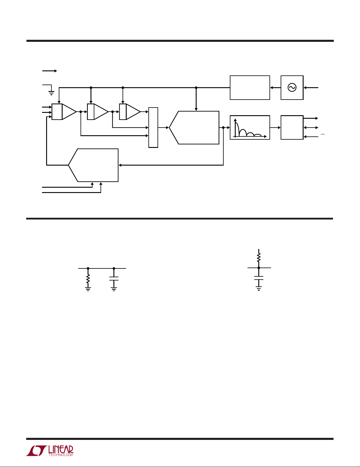
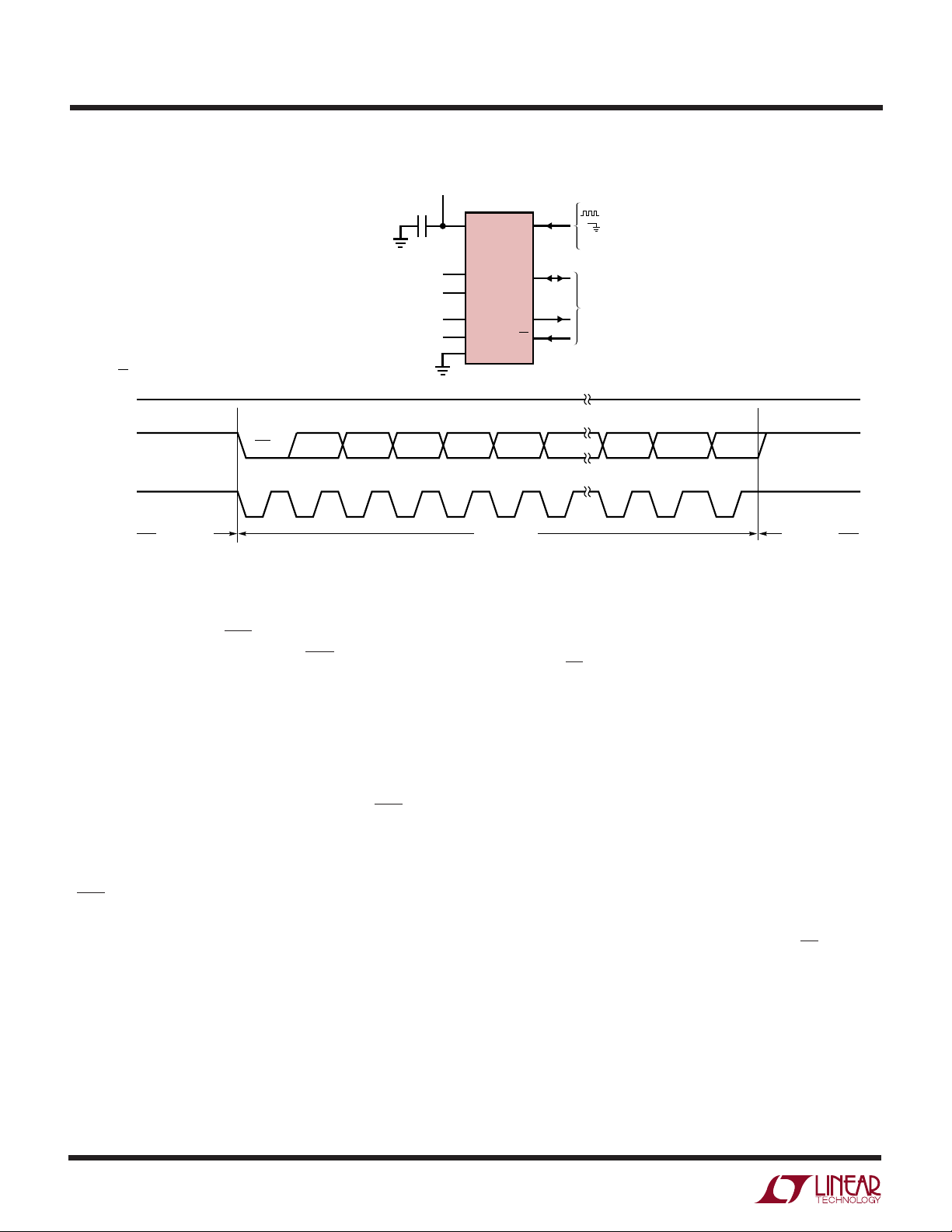
FU CTIO AL DIAGRA
V
CC
GND
+
IN
IN
REF
REF
+
–
–
DAC
+
–
INTERNAL
OSCILLATOR
AUTOCALIBRATION
AND CONTROL
∫∫∫
∑
ADC
DECIMATING FIR
SERIAL
INTERFACE
(INT/EXT)
24331 FD
F
O
SDO
SCK
CS
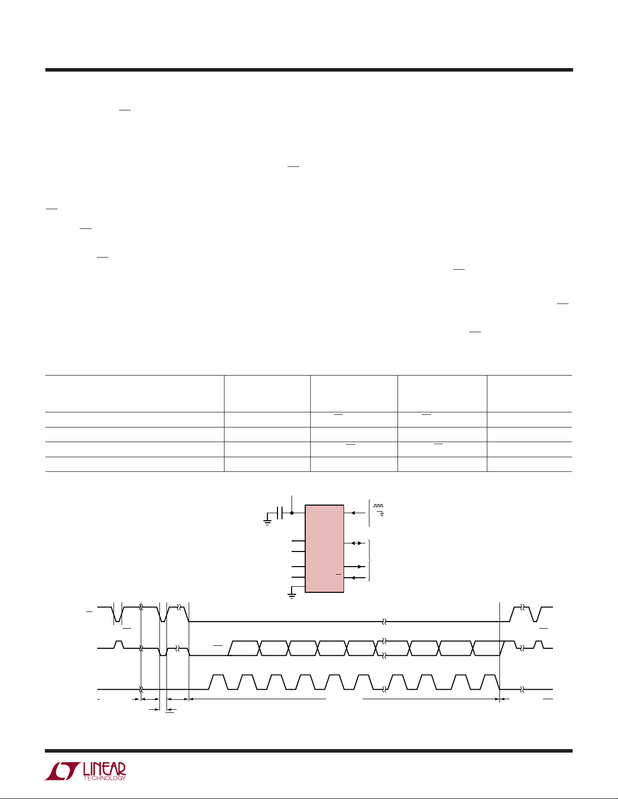
Figure 1. Functional Block Diagram
TEST CIRCUITS
SDO
1.69k
Hi-Z TO V
VOL TO V
OH
VOH TO Hi-Z
= 20pF
C
LOAD
OH
24361 TA03
24331fa
7
Page 8
LTC2433-1
WUUU
APPLICATIO S I FOR ATIO
CONVERTER OPERATION
Converter Operation Cycle
The LTC2433-1 is a low power, ∆Σ ADC with differential
input/reference and an easy-to-use 3-wire serial interface
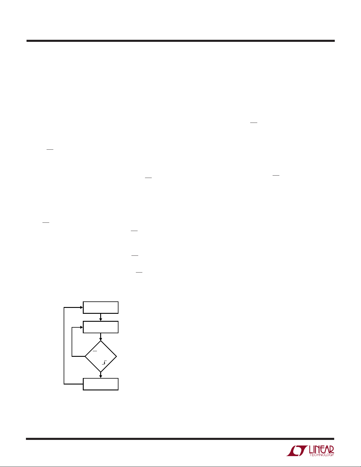
(see Figure 1). Its operation is made up of three states.
The converter operating cycle begins with the conversion,
followed by the low power sleep state and ends with the
data output (see Figure 2). The 3-wire interface consists
of serial data output (SDO), serial clock (SCK) and chip
select (CS).
Initially, the LTC2433-1 performs a conversion. Once the
conversion is complete, the device enters the sleep state.
The part remains in the sleep state as long as CS is HIGH.
While in this sleep state, power consumption is reduced by
nearly two orders of magnitude. The conversion result is
held indefinitely in a static shift register while the converter
is in the sleep state.
Once CS is pulled LOW, the device exits the low power
mode and enters the data output state. If CS is pulled HIGH
before the first rising edge of SCK, the device returns to the
low power sleep mode and the conversion result is still
held in the internal static shift register. If CS remains LOW
after the first rising edge of SCK, the device begins
outputting the conversion result. Taking CS high at this
point will terminate the data output state and start a new
CONVERT
SLEEP
FALSE
CS = LOW
AND
SCK
TRUE
DATA OUTPUT
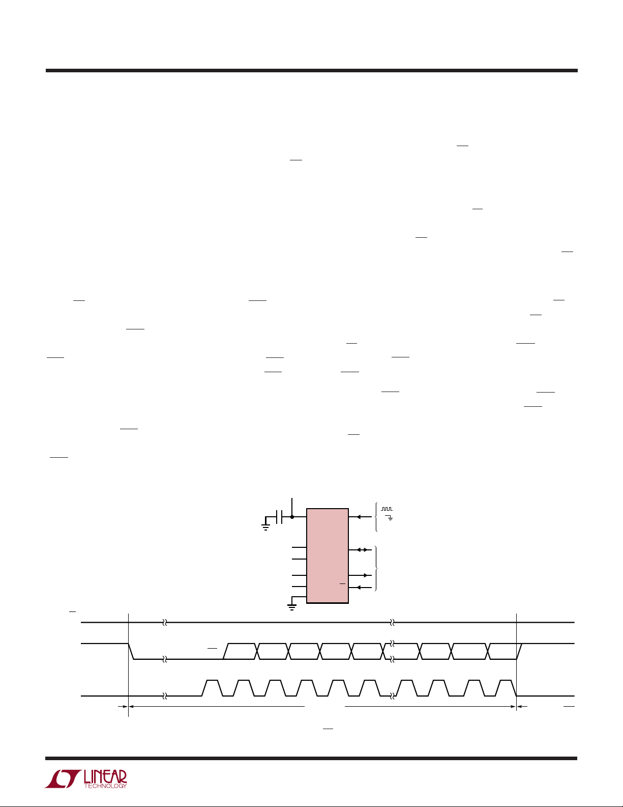
Figure 2. LTC2433-1 State Transition Diagram
24331 F02
conversion. There is no latency in the conversion result.
The data output corresponds to the conversion just performed. This result is shifted out on the serial data out pin
(SDO) under the control of the serial clock (SCK). Data is
updated on the falling edge of SCK allowing the user to
reliably latch data on the rising edge of SCK (see Figure 3).
The data output state is concluded once 19 bits are read
out of the ADC or when CS is brought HIGH. The device
automatically initiates a new conversion and the cycle
repeats. In order to maintain compatibility with 24-/32-bit
data transfers, it is possible to clock the LTC2433-1 with
additional serial clock pulses. This results in additional
data bits which are logic HIGH.
Through timing control of the CS and SCK pins, the
LTC2433-1 offers several flexible modes of operation
(internal or external SCK and free-running conversion
modes). These various modes do not require programming configuration registers; moreover, they do not disturb the cyclic operation described above. These modes of
operation are described in detail in the Serial Interface
Timing Modes section.
Conversion Clock
A major advantage the delta-sigma converter offers over
conventional type converters is an on-chip digital filter
(commonly implemented as a Sinc or Comb filter). For
high resolution, low frequency applications, this filter is
typically designed to reject line frequencies of 50Hz and
60Hz plus their harmonics. The filter rejection performance is directly related to the accuracy of the converter
system clock. The LTC2433-1 incorporates a highly accurate on-chip oscillator. This eliminates the need for external frequency setting components such as crystals or
oscillators. Clocked by the on-chip oscillator, the
LTC2433-1 achieves a minimum of 87dB rejection over
the range 49Hz to 61.2Hz.
Ease of Use
The LTC2433-1 data output has no latency, filter settling
delay or redundant data associated with the conversion
cycle. There is a one-to-one correspondence between the
conversion and the output data. Therefore, multiplexing
multiple analog voltages is easy.
8
24331fa
Page 9

WUUU
APPLICATIO S I FOR ATIO
LTC2433-1
The LTC2433-1 performs offset and full-scale calibrations
every conversion cycle. This calibration is transparent to
the user and has no effect on the cyclic operation described above. The advantage of continuous calibration is
extreme stability of offset and full-scale readings with respect to time, supply voltage change and temperature drift.
Power-Up Sequence
The LTC2433-1 automatically enters an internal reset state
when the power supply voltage VCC drops below approximately 2V. This feature guarantees the integrity of the
conversion result and of the serial interface mode selection. (See the 2-wire I/O sections in the Serial Interface
Timing Modes section.)
When the VCC voltage rises above this critical threshold,
the converter creates an internal power-on-reset (POR)
signal with a typical duration of 1ms. The POR signal clears
all internal registers. Following the POR signal, the
LTC2433-1 starts a normal conversion cycle and follows
the succession of states described above. The first conversion result following POR is accurate within the specifications of the device if the power supply voltage is restored
within the operating range (2.7V to 5.5V) before the end of
the POR time interval.
Reference Voltage Range
This converter accepts a truly differential external reference voltage. The absolute/common mode voltage specification for the REF+ and REF– pins covers the entire range
from GND to VCC. For correct converter operation, the
REF+ pin must always be more positive than the REF– pin.
The LTC2433-1 can accept a differential reference voltage
from 0.1V to VCC. The converter output noise is determined by the thermal noise of the front-end circuits, and
as such, its value in microvolts is nearly constant with
reference voltage. A decrease in reference voltage will
significantly improve the converter’s effective resolution,
since the thermal noise (1.45µV) is well below the quan-
tization level of the device (75.6µV for a 5V reference). At
the minimum reference (100mV) the thermal noise
remains constant at 1.45µV RMS (or 8.7µV
quantization is reduced to 1.5µV per LSB. As a result,
lowering the reference improves the effective resolution
for low level input voltages.
Input Voltage Range
The analog input is truly differential with an absolute/
common mode range for the IN+ and IN– input pins
extending from GND – 0.3V to VCC + 0.3V. Outside these
limits, the ESD protection devices begin to turn on and the
errors due to input leakage current increase rapidly. Within
these limits, the LTC2433-1 converts the bipolar differential input signal, VIN = IN+ – IN–, from – FS = – 0.5 • V
+FS = 0.5 • V
range, the converter indicates the overrange or the
underrange condition using distinct output codes.
Input signals applied to the analog input pins may extend
by 300mV below ground and above VCC. In order to limit
any fault current, resistors of up to 5k may be added in
series with the pins without affecting the performance of
the device. In the physical layout, it is important to maintain the parasitic capacitance of the connection between
these series resistors and the corresponding pins as low
as possible; therefore, the resistors should be located as
close as practical to the pins. The effect of the series
resistance on the converter accuracy can be evaluated
from the curves presented in the Input Current/Reference
Current sections. In addition, series resistors will introduce a temperature dependent offset error due to the input
leakage current. A 10nA input leakage current will develop
a 1LSB offset error on an 8k resistor if V
has a very strong temperature dependency.
Output Data Format
The LTC2433-1 serial output data stream is 19 bits long.
The first 3 bits represent status information indicating the
conversion state and sign. The next 16 bits are the conversion result, MSB first. The third and fourth bit together are
also used to indicate an underrange condition (the differential input voltage is below –FS) or an overrange condition (the differential input voltage is above +FS).
where V
REF
= REF+ – REF–. Outside this
REF
REF
), while the
P-P
to
REF
= 5V. This error
24331fa
9
Page 10
LTC2433-1
WUUU
APPLICATIO S I FOR ATIO
Bit 18 (first output bit) is the end of conversion (EOC)
indicator. This bit is available at the SDO pin during the
conversion and sleep states whenever the CS pin is LOW.
This bit is HIGH during the conversion and goes LOW
when the conversion is complete.
Bit 17 (second output bit) is a dummy bit (DMY) and is
always LOW.
Bit 16 (third output bit) is the conversion result sign indicator (SIG). If VIN is >0, this bit is HIGH. If VIN is <0, this
bit is LOW.
Bit 15 (fourth output bit) is the most significant bit (MSB)
of the result. This bit in conjunction with Bit 16 also
provides the underrange or overrange indication. If both
Bit 16 and Bit 15 are HIGH, the differential input voltage is
above +FS. If both Bit 16 and Bit 15 are LOW, the
differential input voltage is below –FS.
The function of these bits is summarized in Table 1.
Table 1. LTC2433-1 Status Bits
Bit 18 Bit 17 Bit 16 Bit 15
Input Range EOC DMY SIG MSB
VIN ≥ 0.5 • V
0V ≤ VIN < 0.5 • V
–0.5 • V
VIN < –0.5 • V
REF
≤ VIN < 0V 0001
REF
REF
REF
0011
0010
0000
Bits 15-0 are the 16-Bit conversion result MSB first.
Bit 0 is the least significant bit (LSB).
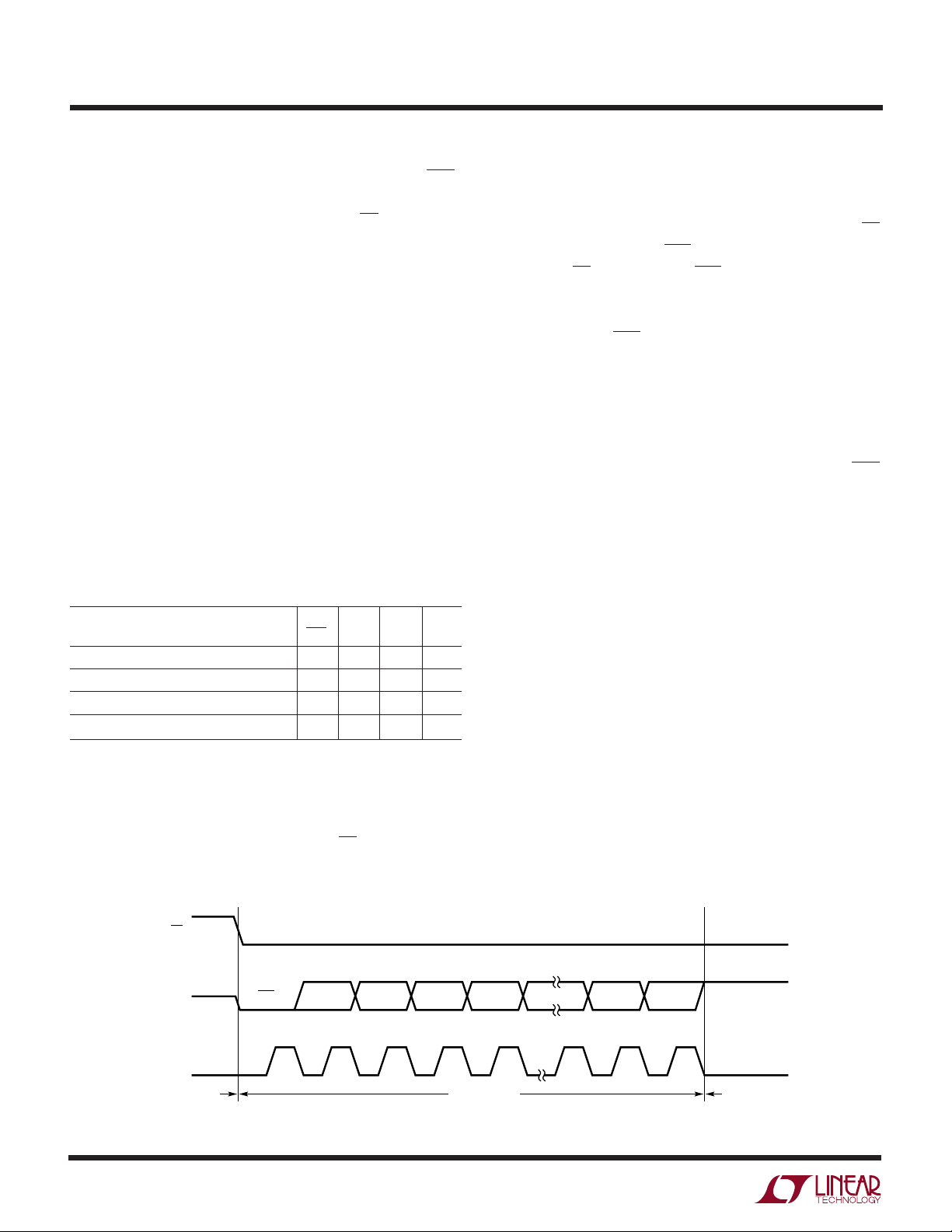
Data is shifted out of the SDO pin under control of the serial
clock (SCK), see Figure 3. Whenever CS is HIGH, SDO
remains high impedance and any externally generated
SCK clock pulses are ignored by the internal data out shift
register.
In order to shift the conversion result out of the device, CS
must first be driven LOW. EOC is seen at the SDO pin of the
device once CS is pulled LOW. EOC changes real time from
HIGH to LOW at the completion of a conversion. This
signal may be used as an interrupt for an external microcontroller. Bit 18 (EOC) can be captured on the first rising
edge of SCK. Bit 17 is shifted out of the device on the first
falling edge of SCK. The final data bit (Bit 0) is shifted out
on the falling edge of the 18th SCK and may be latched on
the rising edge of the 19th SCK pulse. On the falling edge
of the 19th SCK pulse, SDO goes HIGH indicating the
initiation of a new conversion cycle. This bit serves as EOC
(Bit 18) for the next conversion cycle. Table 2 summarizes
the output data format.
In order to remain compatible with some SPI
microcontrollers, more than 19 SCK clock pulses may be
applied. As long as these clock edges are complete before
the conversion ends, they will not effect the serial data.
However, switching SCK during a conversion may generate ground currents in the device leading to extra offset
and noise error sources.
As long as the voltage on the analog input pins is maintained within the – 0.3V to (VCC + 0.3V) absolute maximum
operating range, a conversion result is generated for any
differential input voltage VIN from –FS = –0.5 • V
+FS = 0.5 • V
. For differential input voltages greater than
REF
REF
to
+FS, the conversion result is clamped to the value corresponding to the +FS + 1LSB. For differential input voltages
below –FS, the conversion result is clamped to the value
corresponding to –FS – 1LSB.
10
SDO
SCK
CS
BIT 0BIT 14 BIT 1
LSB
16
24331 F03
24331fa
Hi-Z
SLEEP
BIT 18
EOC
1 2 3 4 5 171819
BIT 15BIT 16BIT 17
MSBSIG“O”
DATA OUTPUT CONVERSION
Figure 3. Output Data Timing
Page 11
WUUU
APPLICATIO S I FOR ATIO
Table 2. LTC2433-1 Output Data Format
Differential Input Voltage Bit 18 Bit 17 Bit 16 Bit 15 Bit 14 Bit 13 Bit 12 … Bit 0
* EOC DMY SIG MSB
V
IN
VIN* ≥ 0.5 • V
0.5 • V
REF
0.25 • V
REF
0.25 • V
REF
0 00100 0 0…0
–1LSB 0 0011 1 1…1
–0.25 • V
–0.25 • V
–0.5 • V
VIN* < –0.5 • V
*The differential input voltage VIN = IN+ – IN–.
**The differential reference voltage V
** 0 0110 0 0…0
REF
** – 1LSB 00101 1 1…1
** 00101 0 0…0
** – 1LSB 0 0100 1 1…1
** 00011 0 0…0
REF
** – 1LSB 00010 1 1…1
REF
** 00010 0 0…0
REF
** 0 0001 1 1…1
REF
= REF+ – REF–.
REF
LTC2433-1
–80
–90
–100
–100
–120
–130
NORMAL MODE REECTION RATIO (dB)
–140
48 50 52 54 56 58 60 62
DIFFERENTIAL INPUT SIGNAL FREQUENCY (Hz)
24361 F04
Figure 4. LTC2433-1 Normal Mode
Rejection When Using an Internal Oscillator
Simultaneous Frequency Rejection
The LTC2433-1 internal oscillator provides better than
87dB normal mode rejection over the range of 49Hz to
61.2Hz as shown in Figure 4. For this simultaneous 50Hz/
60Hz rejection, FO should be connected to GND.
When a fundamental rejection frequency different from
the range 49Hz to 61.2Hz is required or when the converter
must be sychronized with an outside source, the LTC2433-1
can operate with an external conversion clock. The conveter
automatically detects the presence of an external clock
signal at the FO pin and turns off the internal oscillator. The
frequency f
of the external signal must be at least
EOSC
–80
–85
–90
–95
–100
–105
–110
–115
–120
–125
NORMAL MODE REJECTION (dB)
–130
–135
–140
–12–8–404812
DIFFERENTIAL INPUT SIGNAL FREQUENCY
DEVIATION FROM NOTCH FREQUENCY f
EOSC
/2560(%)
24361 F05
Figure 5. LTC2433-1 Normal Mode Rejection When
Using an External Oscillator of Frequency f
EOSC
2560Hz to be detected. The external clock signal duty cycle
is not significant as long as the minimum and maximum
specifications for the high and low periods, t
HEO
and t
LEO
,
are observed.
While operating with an external conversion clock of a
frequency f
normal mode rejection in a frequency range f
, the LTC2433-1 provides better than 110dB
EOSC
EOSC
/2560
±4%. The normal mode rejection as a function of the input
frequency deviation from f
/2560 is shown in Figure 5.
EOSC
Whenever an external clock is not present at the FO pin the
converter automatically activates its internal oscillator and
enters the Internal Conversion Clock mode. The LTC2433-1
24331fa
11
Page 12
LTC2433-1
WUUU
APPLICATIO S I FOR ATIO
operation will not be disturbed if the change of conversion
clock source occurs during the sleep state or during the
data output state while the converter uses an external
serial clock. If the change occurs during the conversion
state, the result of the conversion in progress may be
outside specifications but the following conversions will
not be affected. If the change occurs during the data output
state and the converter is in the Internal SCK mode, the
serial clock duty cycle may be affected but the serial data
stream will remain valid.
Table 3 summarizes the duration of each state and the
achievable output data rate as a function of FO.
SERIAL INTERFACE PINS
The LTC2433-1 transmits the conversion results and
receives the start of conversion command through a
synchronous 3-wire interface. During the conversion and
sleep states, this interface can be used to assess the
converter status and during the data output state it is used
to read the conversion result.
Serial Clock Input/Output (SCK)
dividing the internal conversion clock by 8. In the External
SCK mode of operation, the SCK pin is used as input. The
internal or external SCK mode is selected on power-up and
then reselected every time a HIGH-to-LOW transition is
detected at the CS pin. If SCK is HIGH or floating at powerup or during this transition, the converter enters the internal SCK mode. If SCK is LOW at power-up or during this
transition, the converter enters the external SCK mode.
Serial Data Output (SDO)
The serial data output pin, SDO (Pin 8), provides the result
of the last conversion as a serial bit stream (MSB first)
during the data output state. In addition, the SDO pin is
used as an end of conversion indicator during the conversion and sleep states.
When CS (Pin 7) is HIGH, the SDO driver is switched to a
high impedance state. This allows sharing the serial
interface with other devices. If CS is LOW during the
convert or sleep state, SDO will output EOC. If CS is LOW
during the conversion phase, the EOC bit appears HIGH on
the SDO pin. Once the conversion is complete, EOC goes
LOW.
The serial clock signal present on SCK (Pin 9) is used to
Chip Select Input (CS)
synchronize the data transfer. Each bit of data is shifted out
the SDO pin on the falling edge of the serial clock.
In the Internal SCK mode of operation, the SCK pin is an
The active LOW chip select, CS (Pin 7), is used to test the
conversion status and to enable the data output transfer as
described in the previous sections.
output and the LTC2433-1 creates its own serial clock by
Table 3. LTC2433-1 State Duration
State Operating Mode Duration
CONVERT Internal Oscillator FO = LOW 147ms, Output Data Rate ≤ 6.8 Readings/s
Simultaneous 50Hz/60Hz Rejection
External Oscillator FO = External Oscillator 20510/f
with Frequency f
/2560 Rejection)
(f
EOSC
SLEEP As Long As CS = HIGH Until CS = LOW and SCK
DATA OUTPUT Internal Serial Clock FO = LOW As Long As CS = LOW But Not Longer Than 1.09ms
(Internal Oscillator) (19 SCK cycles)
FO = External Oscillator with As Long As CS = LOW But Not Longer Than 152/f
Frequency f
External Serial Clock with As Long As CS = LOW But Not Longer Than 19/f
Frequency f
kHz (19 SCK cycles)
SCK
EOSC
kHz
EOSC
kHz (19 SCK cycles)
s, Output Data Rate ≤ f
EOSC
/20510 Readings/s
EOSC
EOSC
SCK
ms
ms
12
24331fa
Page 13
WUUU
APPLICATIO S I FOR ATIO
LTC2433-1
In addition, the CS signal can be used to trigger a new
conversion cycle before the entire serial data transfer has
been completed. The LTC2433-1 will abort any serial data
transfer in progress and start a new conversion cycle
anytime a LOW-to-HIGH transition is detected at the CS
pin after the converter has entered the data output state
(i.e., after the first rising edge of SCK occurs with
operation. These include internal/external serial clock,
2- or 3-wire I/O, single cycle conversion and autostart. The
following sections describe each of these serial interface
timing modes in detail. In all these cases, the converter
can use the internal oscillator (FO = LOW) or an external
oscillator connected to the FO pin. Refer to Table␣ 4 for a
summary.
CS␣=␣LOW).
Finally, CS can be used to control the free-running modes
External Serial Clock, Single Cycle Operation
(SPI/MICROWIRE Compatible)
of operation, see Serial Interface Timing Modes section.
Grounding CS will force the ADC to continuously convert
at the maximum output rate selected by FO.
This timing mode uses an external serial clock to shift out
the conversion result and a CS signal to monitor and
control the state of the conversion cycle, see Figure 6.
SERIAL INTERFACE TIMING MODES
The LTC2433-1’s 3-wire interface is SPI and MICROWIRE
compatible. This interface offers several flexible modes of
Table 4. LTC2433-1 Interface Timing Modes
SCK Cycle Output and
Configuration Source Control Control Waveforms
External SCK, Single Cycle Conversion External CS and SCK CS and SCK Figures 6, 7
External SCK, 2-Wire I/O External SCK SCK Figure 8
Internal SCK, Single Cycle Conversion Internal CS ↓ CS ↓ Figures 9, 10
Internal SCK, 2-Wire I/O, Continuous Conversion Internal Continuous Internal Figure 11
The serial clock mode is selected on the falling edge of CS.
To select the external serial clock mode, the serial clock pin
(SCK) must be LOW during each CS falling edge.
Conversion Data Connection
SDO
SCK
(EXTERNAL)
CS
TEST EOC
CONVERSION
SLEEP
TEST EOC
(OPTIONAL)
2.7V TO 5.5V
1µF
110
V
F
CC
O
LTC2433-1
2
+
9
SCK
–
8
SDO
7
CS
DATA OUTPUT CONVERSION
SLEEP
BIT 18
EOC
REFERENCE
VOLTAGE
0.1V TO V
ANALOG INPUT RANGE
–0.5V
TO 0.5V
REF
REF
3
REF
CC
4
+
IN
REF
5
–
IN
6
GND
MSBSIG“O”
Figure 6. External Serial Clock, Single Cycle Operation
= EXTERNAL CLOCK SOURCE
= INTERNAL OSC/SIMULTANEOUS
50Hz/60Hz REJECTION
3-WIRE
SPI INTERFACE
BIT 2 BIT 1BIT 14 BIT 13BIT 15BIT 16BIT 17
BIT 0
LSB
TEST EOC
Hi-ZHi-ZHi-Z
24331 F06
24331fa
13
Page 14

LTC2433-1
WUUU
APPLICATIO S I FOR ATIO
The serial data output pin (SDO) is Hi-Z as long as CS is
HIGH. At any time during the conversion cycle, CS may be
pulled LOW in order to monitor the state of the converter.
While CS is pulled LOW, EOC is output to the SDO pin.
EOC␣ =␣ 1 while a conversion is in progress and EOC = 0 if
the device is in the sleep state. With CS high, the device
automatically enters the low power sleep state once the
conversion is complete.
When the device is in the sleep state (EOC = 0), its
conversion result is held in an internal static shift register. Data is
shifted out the SDO pin on each falling edge of
SCK. This enables external circuitry to latch the output on
the rising edge of SCK. EOC can be latched on the first
rising edge of SCK and the last bit of the conversion result
can be latched on the 19th rising edge of SCK. On the 19th
falling edge of SCK, the device begins a new conversion.
2.7V TO 5.5V
1µF
110
REF
2
3
CC
4
5
6
REFERENCE
VOLTAGE
0.1V TO V
ANALOG INPUT RANGE
–0.5V
REF
TO 0.5V
SDO goes HIGH (EOC = 1) indicating a conversion is in
progress.
At the conclusion of the data cycle, CS may remain LOW
and EOC monitored as an end-of-conversion interrupt.
Alternatively, CS may be driven HIGH setting SDO to Hi-Z.
As described above, CS may be pulled LOW at any time in
order to monitor the conversion status.
Typically, CS remains LOW during the data output state.
However, the data output state may be aborted by pulling
CS HIGH anytime between the first rising edge and the
19th falling edge of SCK, see Figure 7. On the rising edge
of CS, the device aborts the data output state and immediately initiates a new conversion. This is useful for aborting an invalid conversion cycle or synchronizing the start
of a conversion.
V
CC
LTC2433-1
+
REF
–
REF
+
IN
–
IN
GND
SCK
SDO
F
O
9
8
7
CS
= EXTERNAL CLOCK SOURCE
= INTERNAL OSC/SIMULTANEOUS
50Hz/60Hz REJECTION
3-WIRE
SPI INTERFACE
(EXTERNAL)
14
CS
SDO
SCK
SLEEP
EOC
DATA
OUTPUT
TEST EOC
CONVERSION
BIT 18BIT 0
Hi-Z
SLEEP
TEST EOC (OPTIONAL)
Hi-Z Hi-ZHi-Z
SLEEP
EOC
MSBSIG“O”
DATA OUTPUT
Figure 7. External Serial Clock, Reduced Data Output Length
BIT 4BIT 14 BIT 5BIT 15BIT 16BIT 17
TEST EOC
CONVERSION
24331 F07
24331fa
Page 15
WUUU
APPLICATIO S I FOR ATIO
LTC2433-1
External Serial Clock, 2-Wire I/O
This timing mode utilizes a 2-wire serial I/O interface. The
conversion result is shifted out of the device by an externally generated serial clock (SCK) signal, see Figure 8. CS
may be permanently tied to ground, simplifying the user
interface or isolation barrier.
The external serial clock mode is selected at the end of the
power-on reset (POR) cycle. The POR cycle is concluded
typically 1ms after VCC exceeds 2V. The level applied to
SCK at this time determines if SCK is internal or external.
SCK must be driven LOW prior to the end of POR in order
to enter the external serial clock timing mode.
Since CS is tied LOW, the end-of-conversion (EOC) can be
continuously monitored at the SDO pin during the convert
and sleep states. EOC may be used as an interrupt to an
external controller indicating the conversion result is ready.
EOC = 1 while the conversion is in progress and EOC␣ =␣ 0
once the conversion ends. On the falling edge of EOC, the
conversion result is loaded into an internal static shift register. Data is shifted out the SDO pin on each falling edge
of SCK enabling external circuitry to latch data on the rising edge of SCK. EOC can be latched on the first rising edge
of SCK. On the 19th falling edge of SCK, SDO goes HIGH
(EOC␣ =␣ 1) indicating a new conversion has begun.
Internal Serial Clock, Single Cycle Operation
This timing mode uses an internal serial clock to shift out
the conversion result and a CS signal to monitor and
control the state of the conversion cycle, see Figure 9.
In order to select the internal serial clock timing mode, the
serial clock pin (SCK) must be floating (Hi-Z) or pulled
HIGH prior to the falling edge of CS. The device will not
enter the internal serial clock mode if SCK is driven LOW
on the falling edge of CS. An internal weak pull-up resistor
is active on the SCK pin during the falling edge of CS;
therefore, the internal serial clock timing mode is automatically selected if SCK is not externally driven.
The serial data output pin (SDO) is Hi-Z as long as CS is
HIGH. At any time during the conversion cycle, CS may be
pulled LOW in order to monitor the state of the converter.
Once CS is pulled LOW, SCK goes LOW and EOC is output
to the SDO pin. EOC = 1 while a conversion is in progress
and EOC = 0 if the device is in the sleep state.
When testing EOC, if the conversion is complete (EOC = 0),
the device will exit the sleep state during the EOC test. In
order to allow the device to return to the low power sleep
state, CS must be pulled HIGH before the first rising edge
of SCK. In the internal SCK timing mode, SCK goes HIGH
SDO
SCK
(EXTERNAL)
CS
CONVERSION
2.7V TO 5.5V
BIT 18
EOC
1µF
REFERENCE
VOLTAGE
0.1V TO V
ANALOG INPUT RANGE
TO 0.5V
–0.5V
REF
110
V
2
REF
3
REF
CC
4
IN
REF
5
IN
6
GND
MSBSIG“O”
DATA OUTPUT CONVERSION
CC
LTC2433-1
+
–
+
–
SCK
SDO
F
O
9
8
7
CS
= EXTERNAL CLOCK SOURCE
= INTERNAL OSC/SIMULTANEOUS
50Hz/60Hz REJECTION
3-WIRE
SPI INTERFACE
Figure 8. External Serial Clock, CS = 0 Operation (2-Wire)
BIT 2 BIT 1BIT 14 BIT 13BIT 15BIT 16BIT 17
BIT 0
LSB
24331 F08
24331fa
15
Page 16

LTC2433-1
WUUU
APPLICATIO S I FOR ATIO
ANALOG INPUT RANGE
–0.5V
<t
EOCtest
CS
BIT 18
SDO
SCK
(INTERNAL)
Hi-Z Hi-Z Hi-Z Hi-Z
SLEEP
EOC
SLEEP
REFERENCE
0.1V TO V
TO 0.5V
REF
2.7V TO 5.5V
1µF
VOLTAGE
110
V
F
CC
O
LTC2433-1
2
+
REF
3
REF
CC
4
+
IN
REF
5
–
IN
6
GND
MSBSIG“O”
9
SCK
–
8
SDO
7
CS
BIT 14 BIT 13BIT 15BIT 16BIT 17
DATA OUTPUT CONVERSIONCONVERSION
= EXTERNAL CLOCK SOURCE
= INTERNAL OSC/SIMULTANEOUS
50Hz/60Hz REJECTION
3-WIRE
SPI INTERFACE
BIT 2 BIT 1
V
CC
10k
BIT 0
LSB
TEST EOC
24331 F09
TEST EOC
(OPTIONAL)
Figure 9. Internal Serial Clock, Single Cycle Operation
and the device begins outputting data at time t
the falling edge of CS (if EOC = 0) or t
after EOC goes
EOCtest
EOCtest
after
LOW (if CS is LOW during the falling edge of EOC). The
value of t
is 23µs if the device is using its internal
EOCtest
oscillator (F0 = logic LOW). If FO is driven by an external
oscillator of frequency f
CS is pulled HIGH before time t
EOSC
, then t
EOCtest
is 3.6/f
EOCtest
EOSC
, the device returns
. If
to the sleep state and the conversion result is held in the
internal static shift register.
If CS remains LOW longer than t
, the first rising
EOCtest
edge of SCK will occur and the conversion result is serially
shifted out of the SDO pin. The data output cycle concludes
after the 19th rising edge. Data is shifted out the SDO pin
on each falling edge of SCK. The internally generated serial
clock is output to the SCK pin. This signal may be used to
shift the conversion result into external circuitry. EOC can
be latched on the first rising edge of SCK and the last bit
of the conversion result on the 19th rising edge of SCK.
After the 19th rising edge, SDO goes HIGH (EOC = 1), SCK
stays HIGH and a new conversion starts.
Typically, CS remains LOW during the data output state.
However, the data output state may be aborted by pulling
CS HIGH anytime between the first and 19th rising edge of
SCK, see Figure 10. On the rising edge of CS, the device
aborts the data output state and immediately initiates a
new conversion. This is useful for aborting an invalid
conversion cycle, or synchronizing the start of a conversion. If CS is pulled HIGH while the converter is driving
SCK LOW, the internal pull-up is not available to restore
SCK to a logic HIGH state. This will cause the device to exit
the internal serial clock mode on the next falling edge of
CS. This can be avoided by adding an external 10k pull-up
resistor to the SCK pin or by never pulling CS HIGH when
SCK is LOW.
Whenever SCK is LOW, the LTC2433-1’s internal pull-up
at pin SCK is disabled. Normally, SCK is not externally
driven if the device is in the internal SCK timing mode.
However, certain applications may require an external
driver on SCK. If this driver goes Hi-Z after outputting a
LOW signal, the LTC2433-1’s internal pull-up remains
16
24331fa
Page 17

WUUU
APPLICATIO S I FOR ATIO
LTC2433-1
SDO
SCK
(INTERNAL)
2.7V TO 5.5V
1µF
110
V
CC
REF
2
REF
3
REF
CC
4
IN
5
IN
6
GND
REFERENCE
VOLTAGE
0.1V TO V
ANALOG INPUT RANGE
>t
EOCtest
CS
BIT 0
EOC
Hi-Z Hi-Z Hi-Z Hi-Z Hi-Z
DATA
OUTPUT
TEST EOC
SLEEP SLEEP
TEST EOC
(OPTIONAL)
–0.5V
<t
REF
EOCtest
BIT 18
TO 0.5V
EOC
LTC2433-1
+
–
+
–
SCK
SDO
F
O
CS
9
8
7
MSBSIG“O”
DATA OUTPUT
= EXTERNAL CLOCK SOURCE
= INTERNAL OSC/SIMULTANEOUS
50Hz/60Hz REJECTION
3-WIRE
SPI INTERFACE
BIT 14 BIT 13BIT 15BIT 16BIT 17
BIT 2
V
CC
10k
TEST EOC
CONVERSIONCONVERSIONSLEEP
24331 F10
Figure 10. Internal Serial Clock, Reduced Data Output Length
disabled. Hence, SCK remains LOW. On the next falling
edge of CS, the device is switched to the external SCK
timing mode. By adding an external 10k pull-up resistor to
SCK, this pin goes HIGH once the external driver goes
Hi-Z. On the next CS falling edge, the device will remain in
the internal SCK timing mode.
A similar situation may occur during the sleep state when
CS is pulsed HIGH-LOW-HIGH in order to test the
conversion status. If the device is in the sleep state (EOC
= 0), SCK will go LOW. Once CS goes HIGH (within the time
period defined above as t
), the internal pull-up is
EOCtest
activated. For a heavy capacitive load on the SCK pin, the
internal pull-up may not be adequate to return SCK to a
HIGH level before CS goes low again. This is not a concern
under normal conditions where CS remains LOW after
detecting EOC = 0. This situation is easily overcome by
adding an external 10k pull-up resistor to the SCK pin.
Internal Serial Clock, 2-Wire I/O,
Continuous Conversion
This timing mode uses a 2-wire, all output (SCK and SDO)
interface. The conversion result is shifted out of the device
by an internally generated serial clock (SCK) signal, see
Figure 11. CS may be permanently tied to ground, simplifying the user interface or isolation barrier.
The internal serial clock mode is selected at the end of the
power-on reset (POR) cycle. The POR cycle is concluded
approximately 1ms after VCC exceeds 2V. An internal weak
pull-up is active during the POR cycle; therefore, the
internal serial clock timing mode is automatically selected
if SCK is not externally driven LOW (if SCK is loaded such
that the internal pull-up cannot pull the pin HIGH, the
external SCK mode will be selected).
24331fa
17
Page 18
LTC2433-1
WUUU
APPLICATIO S I FOR ATIO
ANALOG INPUT RANGE
–0.5V
REF
CS
2.7V TO 5.5V
1µF
REFERENCE
VOLTAGE
0.1V TO V
TO 0.5V
110
REF
V
2
REF
3
REF
CC
4
IN
5
IN
6
GND
CC
LTC2433-1
+
–
+
–
SCK
SDO
F
O
9
8
7
CS
= EXTERNAL CLOCK SOURCE
= INTERNAL OSC/SIMULTANEOUS
50Hz/60Hz REJECTION
3-WIRE
SPI INTERFACE
SDO
SCK
(INTERNAL)
BIT 18
EOC
Figure 11. Internal Serial Clock, Continuous Operation
During the conversion, the SCK and the serial data output
pin (SDO) are HIGH (EOC = 1). Once the conversion is
complete, SCK and SDO go LOW (EOC = 0) indicating the
conversion has finished and the device has entered the
data output state. The data output cycle begins on the
first rising edge of SCK and ends after the
19th
rising
edge. Data is shifted out the SDO pin on each falling edge
of SCK. The internally generated serial clock is output
to the SCK pin. This signal may be used to shift the
conversion result into external circuitry. EOC can be
latched on the first rising edge of SCK and the last bit of
the conversion result can be latched on the
edge of SCK. After the
19th
rising edge, SDO goes HIGH
19th
rising
(EOC = 1) indicating a new conversion is in progress. SCK
remains HIGH during the conversion.
PRESERVING THE CONVERTER ACCURACY
The LTC2433-1 is designed to reduce as much as possible
the conversion result sensitivity to device decoupling,
PCB layout, antialiasing circuits, line frequency perturbations and so on. Nevertheless, in order to preserve the
accuracy capability of this part, some simple precautions
are desirable.
BIT 2 BIT 1 BIT 0BIT 14 BIT 13BIT 15BIT 16BIT 17
LSBMSBSIG“O”
DATA OUTPUT CONVERSIONCONVERSION
24331 F11
Digital Signal Levels
The LTC2433-1’s digital interface is easy to use. Its digital
inputs (FO, CS and SCK in External SCK mode of operation)
accept standard TTL/CMOS logic levels and the internal
hysteresis receivers can tolerate edge rates as slow as
100µs. However, some considerations are required to take
advantage of the exceptional accuracy and low supply
current of this converter.
The digital output signals (SDO and SCK in Internal SCK
mode of operation) are less of a concern because they are
not generally active during the conversion state.
While a digital input signal is in the range 0.5V to
(VCC␣ –␣ 0.5V), the CMOS input receiver draws additional
current from the power supply. It should be noted that,
when any one of the digital input signals (FO, CS and SCK
in External SCK mode of operation) is within this range, the
LTC2433-1 power supply current may increase even if the
signal in question is at a valid logic level. For micropower
operation, it is recommended to drive all digital input
signals to full CMOS levels [VIL < 0.4V and VOH >
(VCC – 0.4V)].
18
24331fa
Page 19

WUUU
APPLICATIO S I FOR ATIO
LTC2433-1
During the conversion period, the undershoot and/or
overshoot of a fast digital signal connected to the
LTC2433-1 pins may severely disturb the analog to digital
conversion process. Undershoot and overshoot can occur because of the impedance mismatch at the converter
pin when the transition time of an external control signal
is less than twice the propagation delay from the driver to
LTC2433-1. For reference, on a regular FR-4 board, signal
propagation velocity is approximately 183ps/inch for
internal traces and 170ps/inch for surface traces. Thus, a
driver generating a control signal with a minimum transition time of 1ns must be connected to the converter pin
through a trace shorter than 2.5 inches. This problem
becomes particularly difficult when shared control lines
are used and multiple reflections may occur. The solution
is to carefully terminate all transmission lines close to
their characteristic impedance.
Parallel termination near the LTC2433-1 pin will eliminate
this problem but will increase the driver power dissipation.
A series resistor between 27Ω and 56Ω placed near the
driver will also eliminate this problem without additional
power dissipation. The actual resistor value depends upon
the trace impedance and connection topology.
An alternate solution is to reduce the edge rate of the
control signals. It should be noted that using very slow
edges will increase the converter power supply current
during the transition time. The multiple ground pins used
in this package configuration, as well as the differential
input and reference architecture, reduce substantially the
converter’s sensitivity to ground currents.
Particular attention must be given to the connection of the
FO signal when the LTC2433-1 is used with an external
conversion clock. This clock is active during the conversion time and the normal mode rejection provided by the
internal digital filter is not very high at this frequency. A
normal mode signal of this frequency at the converter
reference terminals may result in DC gain and INL errors.
A normal mode signal of this frequency at the converter
input terminals may result in a DC offset error. Such
perturbations may occur due to asymmetric capacitive
coupling between the FO signal trace and the converter
input and/or reference connection traces. An immediate
solution is to maintain maximum possible separation
between the FO signal trace and the input/reference signals. When the FO signal is parallel terminated near the
converter, substantial AC current is flowing in the loop
formed by the FO connection trace, the termination and the
ground return path. Thus, perturbation signals may be
inductively coupled into the converter input and/or reference. In this situation, the user must reduce to a minimum
the loop area for the FO signal as well as the loop area for
the differential input and reference connections.
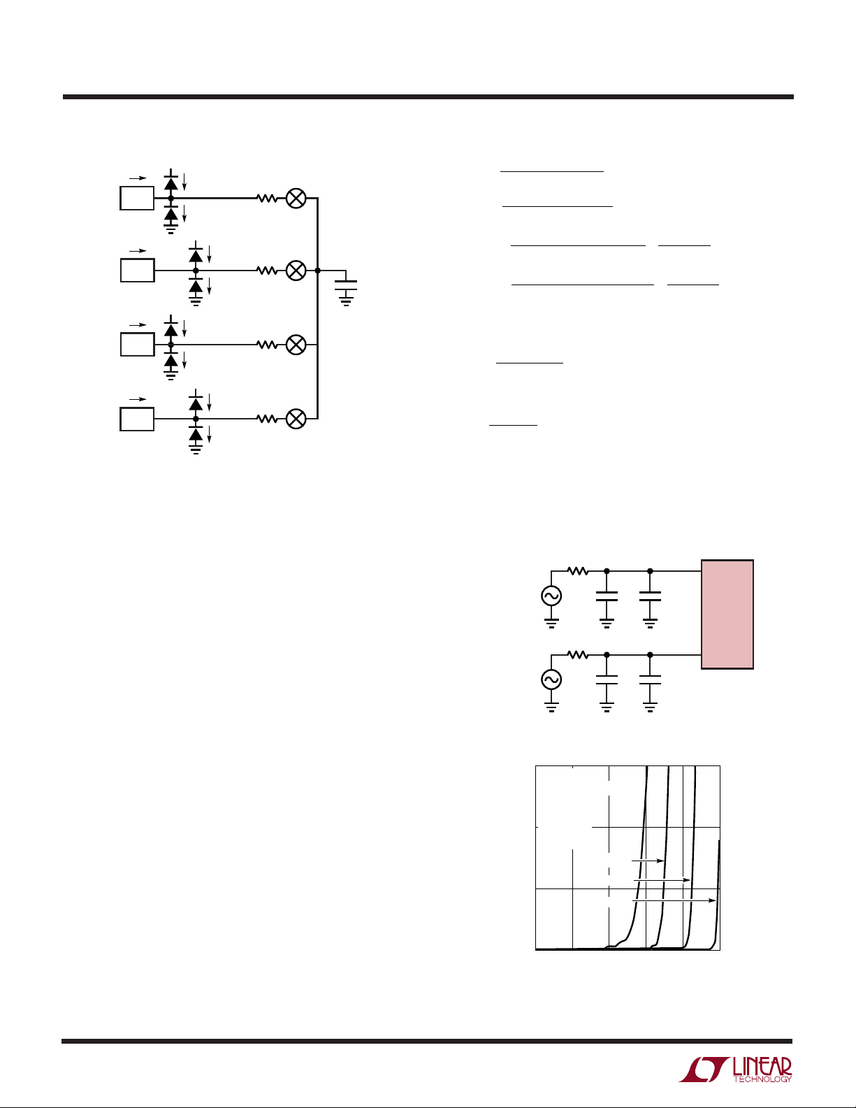
Driving the Input and Reference
The input and reference pins of the LTC2433-1 converter
are directly connected to a network of sampling capacitors. Depending upon the relation between the differential
input voltage and the differential reference voltage, these
capacitors are switching between these four pins
transfering small amounts of charge in the process. A
simplified equivalent circuit is shown in Figure 12, where
IN+ and IN– refer to the selected differential channel and
the unselected channel is omitted for simplicity.
For a simple approximation, the source impedance R
driving an analog input pin (IN+, IN–, REF+ or REF–) can be
considered to form, together with RSW and CEQ (see
Figure␣ 12), a first order passive network with a time
constant τ = (RS + RSW) • CEQ. The converter is able to
sample the input signal with better than 1LSB accuracy if
the sampling period is at least 11 times greater than the
input circuit time constant τ. The sampling process on the
four input analog pins is quasi-independent so each time
constant should be considered by itself and, under worstcase circumstances, the errors may add.
When using the internal oscillator (FO = LOW), the
LTC2433-1’s front-end switched-capacitor network is
clocked at 69900Hz corresponding to a 14.3µs sampling
S
24331fa
19
Page 20
LTC2433-1
WUUU
APPLICATIO S I FOR ATIO
V
CC
I
+
REF
V
+
REF
IIN+
VIN+
IIN–
VIN–
I
–
REF
V
–
REF
SWITCHING FREQUENCY
= 69900Hz INTERNAL OSCILLATOR (FO = LOW)
f
SW
= 0.5 • f
f
SW
I
LEAK
I
LEAK
V
CC
V
CC
I
LEAK
I
LEAK
V
CC
EXTERNAL OSCILLATOR
EOSC
I
LEAK
I
LEAK
I
LEAK
I
LEAK
RSW (TYP)
20k
RSW (TYP)
20k
RSW (TYP)
20k
RSW (TYP)
20k
24331 F12
C
EQ
6pF
(TYP)
VV V
+−
+
IIN
()
−
IIN
()
I REF
()
I REF
()
where
V REF REF
REF
V
REFCM
=−
VININ
IN
V
INCM
==
R M INTERNAL OSCILLATOR Hz Hz Notch F LOW
EQ O
R f EXTERNAL OSCILLATOR
=•
EQ EOSC
IN INCM REFCM
=
AVG
VV V
−+ −
=
AVG
+
=
AVG
−
=
AVG
15
−• − +
R
•
.
05
EQ
IN INCM REFCM
R
•
.
05
EQ
VV V
.
•− +
REF INCM REFCM
R
.
•
05
EQ
VV V
.
15
REF INCM REFCM
R
.
•
05
EQ
2
V
IN
−
VR
•
REF EQ
V
IN
+
VR
REF EQ
2
•
::
+−
=−
+−
REF REF
=
+−
+−
−
IN IN
=
2
./
11 9 50 60
Ω
12
./
167 10
()
+
2
()
Figure 12. LTC2433-1 Equivalent Analog Input Circuit
period. Thus, for settling errors of less than 1LSB, the
driving source impedance should be chosen such that τ ≤
14.3µs/11 = 1.3µs. When an external oscillator of fre-
quency f
for a settling error of less than 1LSB, τ ≤ 0.18/f
is used, the sampling period is 2/f
EOSC
EOSC
EOSC
and,
.
Input Current
If complete settling occurs on the input, conversion results will be unaffected by the dynamic input current. An
incomplete settling of the input signal sampling process
may result in gain and offset errors, but it will not degrade
the INL performance of the converter. Figure 12 shows the
mathematical expressions for the average bias currents
flowing through the IN+ and IN– pins as a result of the
sampling charge transfers when integrated over a substantial time period (longer than 64 internal clock cycles).
The effect of this input dynamic current can be analyzed
using the test circuit of Figure 13. The C
capacitor
PAR
includes the LTC2433-1 pin capacitance (5pF typical) plus
the capacitance of the test fixture used to obtain the results
shown in Figures 14 and 15. A careful implementation can
bring the total input capacitance (CIN + C
) closer to 5pF
PAR
thus achieving better performance than the one predicted
R
SOURCE
V
+ 0.5V
V
INCM
INCM
– 0.5V
IN
R
SOURCE
IN
Figure 13. An RC Network at IN+ and IN
3
VCC = 5V
+
= 5V
REF
–
= GND
REF
+
= 5V
IN
–
= 2.5V
IN
2
= GND
F
O
= 25°C
T
A
C
IN =
C
1
+FS ERROR (LSB)
0
1 10 100 1k 10k 100k
IN =
Figure 14. +FS Error vs R
C
IN =
0.001µF
100pF
C
IN =
R
SOURCE
SOURCE
+
IN
C
(Ω)
PAR
≅20pF
C
PAR
≅20pF
LTC2433-1
–
IN
24331 F14
C
IN
C
IN
0.01µF
0pF
at IN+ or IN– (Small CIN)
24331 F13
–
24331fa
20
Page 21

WUUU
APPLICATIO S I FOR ATIO
LTC2433-1
0
VCC = 5V
+
REF
= 5V
–
= GND
REF
+
= GND
IN
–
IN
–1
= GND
F
O
= 25°C
T
A
–2
–FS ERROR (LSB)
–3
1 10 100 1k 10k 100k
Figure 15. –FS Error vs R
0
)
REF
–4
VCC = 5V
+
REF
–
REF
+
= 1.25V
IN
–FS ERROR (ppm OF V
–
= 3.75V
IN
= GND
F
O
= 25°C
T
A
–8
0
100 200 300 400 500 600 700 800 9001000
Figure 17. –FS Error vs R
= 2.5V
= 5V
= GND
C
C
IN =
C
IN =
IN =
0.001µF
C
IN =
R
SOURCE
R
SOURCE
SOURCE
0pF
100pF
0.01µF
(Ω)
SOURCE
24331 F15
at IN+ or IN– (Small CIN)
C
0.01µF
IN =
C
0.1µF
IN =
C
10µF
IN =
C
1µF
IN =
(Ω)
24331 F17
at IN+ or IN– (Large CIN)
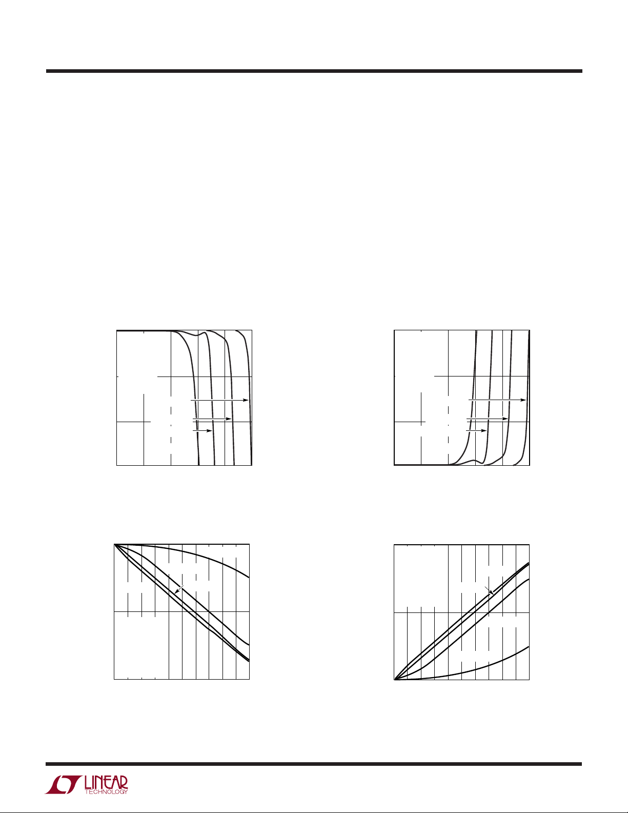
by Figures 14 and 15. For simplicity, two distinct situations can be considered.
For relatively small values of input capacitance (CIN <
0.01µF), the voltage on the sampling capacitor settles
almost completely and relatively large values for the
source impedance result in only small errors. Such values
for CIN will deteriorate the converter offset and gain
performance without significant benefits of signal filtering
and the user is advised to avoid them. Nevertheless, when
small values of CIN are unavoidably present as parasitics
of input multiplexers, wires, connectors or sensors, the
LTC2433-1 can maintain its accuracy while operating with
relative large values of source resistance as shown in
8
VCC = 5V
+
= 5V
REF
–
REF
= GND
+
= 3.75V
IN
–
= 1.25V
IN
= GND
F
O
= 25°C
T
A
4
+FS ERROR (LSB)
0
0
100 200 300 400 500 600 700 800 9001000
R
Figure 16. +FS Error vs R
SOURCE
SOURCE
C
10µF
IN =
C
1µF
IN =
0.1µF
C
IN =
0.01µF
C
IN =
(Ω)
24331 F16
at IN+ or IN– (Large CIN)
Figures 14 and 15. These measured results may be slightly
different from the first order approximation suggested
earlier because they include the effect of the actual second
order input network together with the nonlinear settling
process of the input amplifiers. For small CIN values, the
settling on IN+ and IN– occurs almost independently and
there is little benefit in trying to match the source impedance for the two pins.
Larger values of input capacitors (CIN > 0.01µF) may be
required in certain configurations for antialiasing or general input signal filtering. Such capacitors will average the
input sampling charge and the external source resistance
will see a quasi constant input differential impedance.
When FO = LOW (internal oscillator and 50Hz/60Hz notch),
the typical differential input resistance is 6MΩ which will
generate a gain error of approximately 1LSB at full scale
for each 180Ω of source resistance driving IN+ or IN–.
When FO is driven by an external oscillator with a frequency f
typical differential input resistance is 0.84 • 1012/f
(external conversion clock operation), the
EOSC
EOSC
Ω
and each ohm of source resistance driving IN+ or IN– will
result in 3.7 • 10–8 • f
LSB gain error at full scale. The
EOSC
effect of the source resistance on the two input pins is
additive with respect to this gain error. The typical +FS and
–FS errors as a function of the sum of the source resistance seen by IN+ and IN– for large values of CIN are shown
in Figures 16 and 17.
24331fa
21
Page 22
LTC2433-1
WUUU
APPLICATIO S I FOR ATIO
In addition to this gain error, an offset error term may also
appear. The offset error is proportional with the mismatch
between the source impedance driving the two input pins
IN+ and IN– and with the difference between the input and
reference common mode voltages. While the input drive
circuit nonzero source impedance combined with the converter average input current will not degrade the INL
performance, indirect distortion may result from the modulation of the offset error by the common mode component
of the input signal. Thus, when using large CIN capacitor
values, it is advisable to carefully match the source impedance seen by the IN+ and IN– pins. When FO = LOW
(internal oscillator and 50Hz/60Hz notch), every 180Ω
mismatch in source impedance transforms a full-scale
common mode input signal into a differential mode input
signal of 1LSB. When FO is driven by an external oscillator
with a frequency f
, every 1Ω mismatch in source
EOSC
impedance transforms a full-scale common mode input
signal into a differential mode input signal of 3.7 • 10
• f
LSB. Figure 18 shows the typical offset error due to
EOSC
–8
input common mode voltage for various values of source
resistance imbalance between the IN+ and IN– pins when
large CIN values are used.
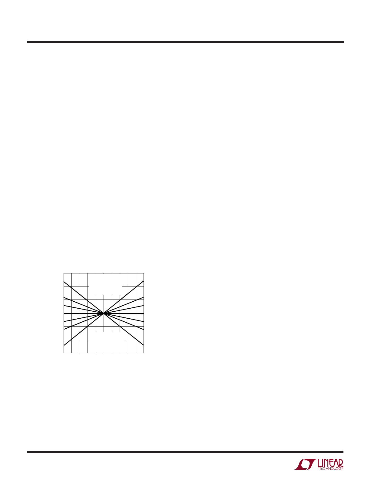
3
A
2
B
1
C
D
0
E
–1
OFFSET ERROR (LSB)
F
–2
G
–3
0.5
0
A: ∆RIN = +400Ω
B: ∆R
C: ∆R
D: ∆R
Figure 18. Offset Error vs Common Mode Voltage
(V
= IN+ = IN–) and Input Source Resistance
INCM
Imbalance (∆RIN = R
Large CIN Values (CIN ≥ 1µF)
1
= +200Ω
IN
= +100Ω
IN
= 0Ω
IN
VCC = 5V
+
= 5V
REF
–
= GND
REF
+
= IN– = V
IN
FO = GND
= 25°C
T
A
R
SOURCEIN
= 10µF
C
IN
21.5
2.5
V
INCM
SOURCEIN
INCM
– = 500Ω
3 3.5 4.5
(V)
E: ∆RIN = –100Ω
F: ∆R
IN
G: ∆R
IN
+ – R
4
= –200Ω
= –400Ω
24331 F18
SOURCEIN
5
–) for
If possible, it is desirable to operate with the input signal
common mode voltage very close to the reference signal
common mode voltage as is the case in the ratiometric
measurement of a symmetric bridge. This configuration
eliminates the offset error caused by mismatched source
impedances.
The magnitude of the dynamic input current depends upon
the size of the very stable internal sampling capacitors and
upon the accuracy of the converter sampling clock. The
accuracy of the internal clock over the entire temperature
and power supply range is typically better than 0.5%. Such
a specification can also be easily achieved by an external
clock. When relatively stable resistors (50ppm/°C) are
used for the external source impedance seen by IN+ and
IN–, the expected drift of the dynamic current, offset and
gain errors will be insignificant (about 1% of their respective values over the entire temperature and voltage range).
Even for the most stringent applications, a one-time
calibration operation may be sufficient.
In addition to the input sampling charge, the input ESD
protection diodes have a temperature dependent leakage
current. This current, nominally 1nA (±10nA max), results
in a small offset shift. A 15k source resistance will create
a 0LSB typical and 1LSB maximum offset voltage.
Reference Current
In a similar fashion, the LTC2433-1 samples the differential reference pins REF+ and REF– transfering small amount
of charge to and from the external driving circuits thus
producing a dynamic reference current. This current does
not change the converter offset, but it may degrade the
gain and INL performance. The effect of this current can be
analyzed in the same two distinct situations.
For relatively small values of the external reference capacitors (C
< 0.01µF), the voltage on the sampling capacitor
REF
settles almost completely and relatively large values for
the source impedance result in only small errors. Such
values for C
will deteriorate the converter offset and
REF
gain performance without significant benefits of reference
filtering and the user is advised to avoid them.
22
24331fa
Page 23
WUUU
APPLICATIO S I FOR ATIO
LTC2433-1
Larger values of reference capacitors (C
> 0.01µF) may
REF
be required as reference filters in certain configurations.
Such capacitors will average the reference sampling charge
and the external source resistance will see a quasi constant reference differential impedance. When FO = LOW
(internal oscillator and 50Hz/60Hz notch), the typical
differential reference resistance is 4.2MΩ which will generate a gain error of approximately 1LSB full scale for each
120Ω of source resistance driving REF+ or REF–. When F
is driven by an external oscillator with a frequency f
O
EOSC
(external conversion clock operation), the typical differential reference resistance is 0.60 • 1012/f
Ω and each
EOSC
ohm of source resistance drving REF+ or REF– will result
in 5.1 • 10–8 • f
+FS ERROR (LSB)
LSB gain error at full scale. The effect
EOSC
0
VCC = 5V
+
= 5V
REF
–
REF
= GND
+
IN
= 3.75V
–
= 1.25V
IN
–1
F
= GND
O
= 25°C
T
A
C
0pF
REF =
C
100pF
–2
–3
1 10 100 1k 10k 100k
C
REF =
REF =
C
REF =
R
0.001µF
0.01µF
SOURCE
(Ω)
24331 F19
of the source resistance on the two reference pins is
additive with respect to this gain error. The typical +FS and
–FS errors for various combinations of source resistance
seen by the REF+ and REF– pins and external capacitance
C
connected to these pins are shown in Figures 19, 20,
REF
21 and␣ 22.
In addition to this gain error, the converter INL perfor-
mance is degraded by the reference source impedance.
When FO = LOW (internal oscillator and 50Hz/60Hz notch),
EOSC
–
O
,
–
every 1000Ω of source resistance driving REF+ or REF
translates into about 1LSB additional INL error. When F
is driven by an external oscillator with a frequency f
every 1000Ω of source resistance driving REF+ or REF
3
VCC = 5V
+
= 5V
REF
–
= GND
REF
+
= 1.25V
IN
–
IN
= 3.75V
2
= GND
F
O
= 25°C
T
A
C
0pF
REF =
C
100pF
1
–FS ERROR (LSB)
0
1 10 100 1k 10k 100k
C
C
REF =
REF =
REF =
0.001µF
0.01µF
R
SOURCE
(Ω)
24331 F20
Figure 19. +FS Error vs R
0
C
= 10µF
REF
–5
VCC = 5V
+
= 5V
REF
+FS ERROR (LSB)
–10
–
= GND
REF
+
= 3.75V
IN
–
= 1.25V
IN
= GND
F
O
= 25°C
T
A
200 400 600 1000700100 300 500 900
0
Figure 21. +FS Error vs R
at REF+ or REF– (Small CIN) Figure 20. –FS Error vs R
SOURCE
C
= 0.01µF
REF
= 0.1µF
C
REF
C
= 1µF
REF
800
R
(Ω)
SOURCE
at REF+ and REF– (Large C
SOURCE
24331 F21
10
5
–FS ERROR (LSB)
0
0
) Figure 22. –FS Error vs R
REF
at REF+ or REF– (Small CIN)
SOURCE
VCC = 5V
+
= 5V
REF
–
REF
= GND
+
= 1.25V
IN
–
= 3.75V
IN
= GND
F
O
= 25°C
T
A
200 400 600 1000700100 300 500 900
C
= 1µF
REF
C
= 0.01µF
REF
R
(Ω)
SOURCE
at REF+ and REF– (Large C
SOURCE
= 10µF
C
REF
C
= 0.1µF
REF
800
24331 F22
)
REF
24331fa
23
Page 24
LTC2433-1
WUUU
APPLICATIO S I FOR ATIO
translates into about 7.15 • 10–6 • f
LSB additional INL
EOSC
error. Figure␣ 23 shows the typical INL error due to the
source resistance driving the REF+ or REF– pins when
large C
values are used. The effect of the source
REF
resistance on the two reference pins is additive with
respect to this INL error. In general, matching of source
impedance for the REF+ and REF– pins does not help the
gain or the INL error. The user is thus advised to minimize
the combined source impedance driving the REF+ and
REF– pins rather than to try to match it.
The magnitude of the dynamic reference current depends
upon the size of the very stable internal sampling capacitors and upon the accuracy of the converter sampling
clock. The accuracy of the internal clock over the entire
temperature and power supply range is typical better than
0.5%. Such a specification can also be easily achieved by
an external clock. When relatively stable resistors
(50ppm/°C) are used for the external source impedance
seen by REF+ and REF–, the expected drift of the dynamic
current gain error will be insignificant (about 1% of its
value over the entire temperature and voltage range). Even
for the most stringent applications a one-time calibration
operation may be sufficient.
1
R
SOURCE
= 1000Ω
In addition to the reference sampling charge, the reference
pins ESD protection diodes have a temperature dependent
leakage current. This leakage current, nominally 1nA
(±10nA max), results in a small gain error. A 100Ω source
resistance will create a 0.05µV typical and 0.5µV maxi-
mum full-scale error.
Output Data Rate
When using its internal oscillator, the LTC2433-1 can
produce up to 6.8 readings per second. The actual output
data rate will depend upon the length of the sleep and data
output phases which are controlled by the user and which
can be made insignificantly short. When operated with an
external conversion clock (FO connected to an external
oscillator), the LTC2433-1 output data rate can be increased as desired. The duration of the conversion phase
is 20510/f
EOSC
. If f
= 139,800Hz, the converter be-
EOSC
haves as if the internal oscillator is used with simultaneous
50Hz/60Hz. There is no significant difference in the
LTC2433-1 performance between these two operation
modes.
An increase in f
over the nominal 139,800Hz will
EOSC
translate into a proportional increase in the maximum
output data rate. This substantial advantage is nevertheless accompanied by three potential effects, which must
be carefully considered.
0
INL (LSB)
–1
–0.5–0.4–0.3–0.2–0.1 0 0.1 0.2 0.3 0.4 0.5
VCC = 5V
REF+ = 5V
REF– = GND
V
INCM
Figure 23. INL vs Differential Input Voltage (VIN = IN+ – IN–)
and Reference Source Resistance (R
for Large C
Values (C
REF
V
INDIF/VREFDIF
= 0.5 • (IN+ + IN–) = 2.5V
≥ 1µF)
REF
FO = GND
= 10µF
C
REF
= 25°C
T
A
at REF+ and REF
SOURCE
24331 F23
24
First, a change in f
will result in a proportional change
EOSC
in the internal notch position and in a reduction of the
converter differential mode rejection at the power line
frequency. In many applications, the subsequent performance degradation can be substantially reduced by relying upon the LTC2433-1’s exceptional common mode
rejection and by carefully eliminating common mode to
differential mode conversion sources in the input circuit.
The user should avoid single-ended input filters and
should maintain a very high degree of matching and
symmetry in the circuits driving the IN+ and IN– pins.
Second, the increase in clock frequency will increase
–
proportionally the amount of sampling charge transferred
through the input and the reference pins. If large external
24331fa
Page 25

WUUU
APPLICATIO S I FOR ATIO
LTC2433-1
input and/or reference capacitors (CIN, C
) are used, the
REF
previous section provides formulae for evaluating the
effect of the source resistance upon the converter performance for any value of f
or reference capacitors (CIN, C
. If small external input and/
EOSC
) are used, the effect of
REF
the external source resistance upon the LTC2433-1 typical
performance can be inferred from Figures 14, 15, 19 and
20 in which the horizontal axis is scaled by 139,800/f
8
VCC = 5V
V
= 5V
REF
= 2.5V
V
INCM
V
= 0V
IN
F
= EXT OSC
O
TA = 85°C
0
OFFSET ERROR (LSB)
–8
10 20 30 40 50 100
0
OUTPUT DATA RATE (READINGS/SEC)
TA = 25°C
60 70 80 90
24331 F24
EOSC
.
Third, an increase in the frequency of the external oscillator above 460800Hz (a more than 3× increase in the output
data rate) will start to decrease the effectiveness of the
internal autocalibration circuits. This will result in a progressive degradation in the converter accuracy and linearity. Typical measured performance curves for output data
rates up to 100 readings per second are shown in Figures␣ 24, 25, 26, 27, 28 and 29. In order to obtain the
15
VCC = 5V
= 5V
V
REF
+
12
= 3.75V
IN
–
= 1.25V
IN
= EXT OSC
F
O
9
6
TA = 85°C
3
+FS ERROR (LSB)
0
–3
TA = 25°C
20 40 60 80
OUTPUT DATA RATE (READINGS/SEC)
10010030507090
24331 F25
Figure 24. Offset Error vs Output Data Rate and Temperature
6
TA = 25°C
3
0
TA = 85°C
–3
–FS ERROR (LSB)
VCC = 5V
= 5V
V
REF
+
–6
IN
= 1.25V
–
= 3.75V
IN
= EXT OSC
F
O
–9
102030
0
OUTPUT DATA RATE (READINGS/SEC)
40
50 60 70 80 90 100
24331 F26
Figure 26. –FS Error vs Output Data Rate and Temperature
Figure 25. +FS Error vs Output Data Rate and Temperature
50
GAUSSIAN DISTRIBUTION
m = 3.1µV
σ = 1.59µV
40
30
20
NUMBER OF READINGS (%)
10
0
RMS
0
1
OUTPUT CODE
–1
2
3
VCC = 5V
= 0.1V
V
REF
= 0V
V
IN
+
= 0.1V
REF
–
= GND
REF
+
= GND
IN
–
= GND
IN
= 2.048MHz
F
O
= 125°C
T
A
4
5
2433 F27
Figure 27. Noise Histogram (Output Rate = 100Hz,
VCC = 5V, V
= 100mV, 125°C)
REF
24331fa
25
Page 26

LTC2433-1
WUUU
APPLICATIO S I FOR ATIO
22
20
18
16
VCC = 5V
14
RESOLUTION (BITS)
+
= 5V
V
REF
–
= GND
V
REF
= 2.5V
V
12
INCM
–2.5V < V
F
10
01030507090
< 2.5V
IN
= EXTERNAL OSCILLATOR
O
20 40 60 80
OUTPUT DATA RATE (READINGS/sec)
100
2433 F28
Figure 28. Integral Nonlinearity vs Output Data Rate
highest possible level of accuracy from this converter at
output data rates above 20 readings per second, the user
is advised to maximize the power supply voltage used and
to limit the maximum ambient operating temperature. In
certain circumstances, a reduction of the differential reference voltage may be beneficial.
Increasing Input Resolution by Reducing Reference
Voltage
The resolution of the LTC2433-1 can be increased by
reducing the reference voltage. It is often necessary to
amplify low level signals to increase the voltage resolution
of ADCs that cannot operate with a low reference voltage.
The LTC2433-1 can be used with reference voltages as low
as 100mV, corresponding to a ±50mV input range with full
16-bit resolution. Reducing the reference voltage is functionally equivalent to amplifying the input signal, however
no amplifier is required.
The LTC2433-1 has a 76µV LSB when used with a 5V
reference, however the thermal noise of the inputs is
1.45µV
and is independent of reference voltage. Thus
RMS
reducing the reference voltage will increase the resolution
at the inputs as long as the LSB voltage is significantly
larger than 1.45µV
. A 570mV reference corresponds
RMS
to a 8.7µV LSB, which is approximately the peak-to-peak
value of the 1.45µV
input thermal noise. At this point,
RMS
3
V
= 2.5V
0
–3
VCC = 5V
–
= GND
REF
OFFSET ERROR (LSB)
–6
V
= 2.5V
INCM
= 0V
V
IN
= EXT OSC
F
O
= 25°C
T
A
–9
20 40 60 80
OUTPUT DATA RATE (READINGS/SEC)
REF
V
= 5V
REF
10010030507090
24331 F29
Figure 29. Offset Error vs Output
Data Rate and Reference Voltage
the output code will be stable to ±1LSB for a fixed input. As
the reference is decreased further, the measured noise will
approach 1.45µV
RMS
.
Figure 30 shows two methods of dividing down the
reference voltage to the LTC2433-1. Where absolute accuracy is required, a precision divider such as the Vishay
MPM series dividers in a SOT-23 package may be used. A
51:1 divider provides a 98mV reference to the LTC2433-1
from a 5V source. The resulting ±49mV input range and
1.5µV LSB is suitable for thermocouple and 10mV full-
scale strain gauge measurements.
If high initial accuracy is not critical, a standard 2%
resistor array such as the Panasonic EXB series may be
used. Single package resistor arrays provide better temperature stability than discrete resistors. An array of eight
resistors can be configured as shown to provide a 294mV
reference to the LTC2433-1 from a 5V source. The fully
differential property of the LTC2433-1 reference terminals
allow the reference voltage to be taken from four central
resistors in the network connected in parallel, minimizing
drift in the presence of thermal gradients. This is an ideal
reference for medium accuracy sensors such as silicon
micromachined pressure and force sensors. These devices typically have accuracies on the order of 2% and fullscale outputs of 50mV to 200mV.
26
24331fa
Page 27
PACKAGE DESCRIPTIO
U
MS Package
10-Lead Plastic MSOP
(Reference LTC DWG # 05-08-1661)
0.889
± 0.127
(.035 ± .005)
LTC2433-1
5.23
(.206)
MIN
0.305 ± 0.038
(.0120 ± .0015)
TYP
RECOMMENDED SOLDER PAD LAYOUT
0.254
(.010)
GAUGE PLANE
0.18
(.007)
NOTE:
1. DIMENSIONS IN MILLIMETER/(INCH)
2. DRAWING NOT TO SCALE
3. DIMENSION DOES NOT INCLUDE MOLD FLASH, PROTRUSIONS OR GATE BURRS.
MOLD FLASH, PROTRUSIONS OR GATE BURRS SHALL NOT EXCEED 0.152mm (.006") PER SIDE
4. DIMENSION DOES NOT INCLUDE INTERLEAD FLASH OR PROTRUSIONS.
INTERLEAD FLASH OR PROTRUSIONS SHALL NOT EXCEED 0.152mm (.006") PER SIDE
5. LEAD COPLANARITY (BOTTOM OF LEADS AFTER FORMING) SHALL BE 0.102mm (.004") MAX
3.2 – 3.45
(.126 – .136)
DETAIL “A”
DETAIL “A”
0.50
(.0197)
BSC
° – 6° TYP
0
(.021 ± .006)
0.53 ± 0.01
SEATING
PLANE
3.00 ± 0.102
(.118 ± .004)
(NOTE 3)
4.90 ± 0.15
(1.93 ± .006)
(.043)
0.17 – 0.27
(.007 – .011)
TYP
1.10
MAX
12
0.50
(.0197)
BSC
0.497 ± 0.076
7
6
45
(.0196 ± .003)
REF
3.00 ± 0.102
(.118 ± .004)
NOTE 4
0.86
(.034)
REF
0.13 ± 0.076
(.005 ± .003)
MSOP (MS) 0802
8910
3
Information furnished by Linear Technology Corporation is believed to be accurate and reliable.
However, no responsibility is assumed for its use. Linear Technology Corporation makes no representation that the interconnection of its circuits as described herein will not infringe on existing patent rights.
24331fa
27
Page 28
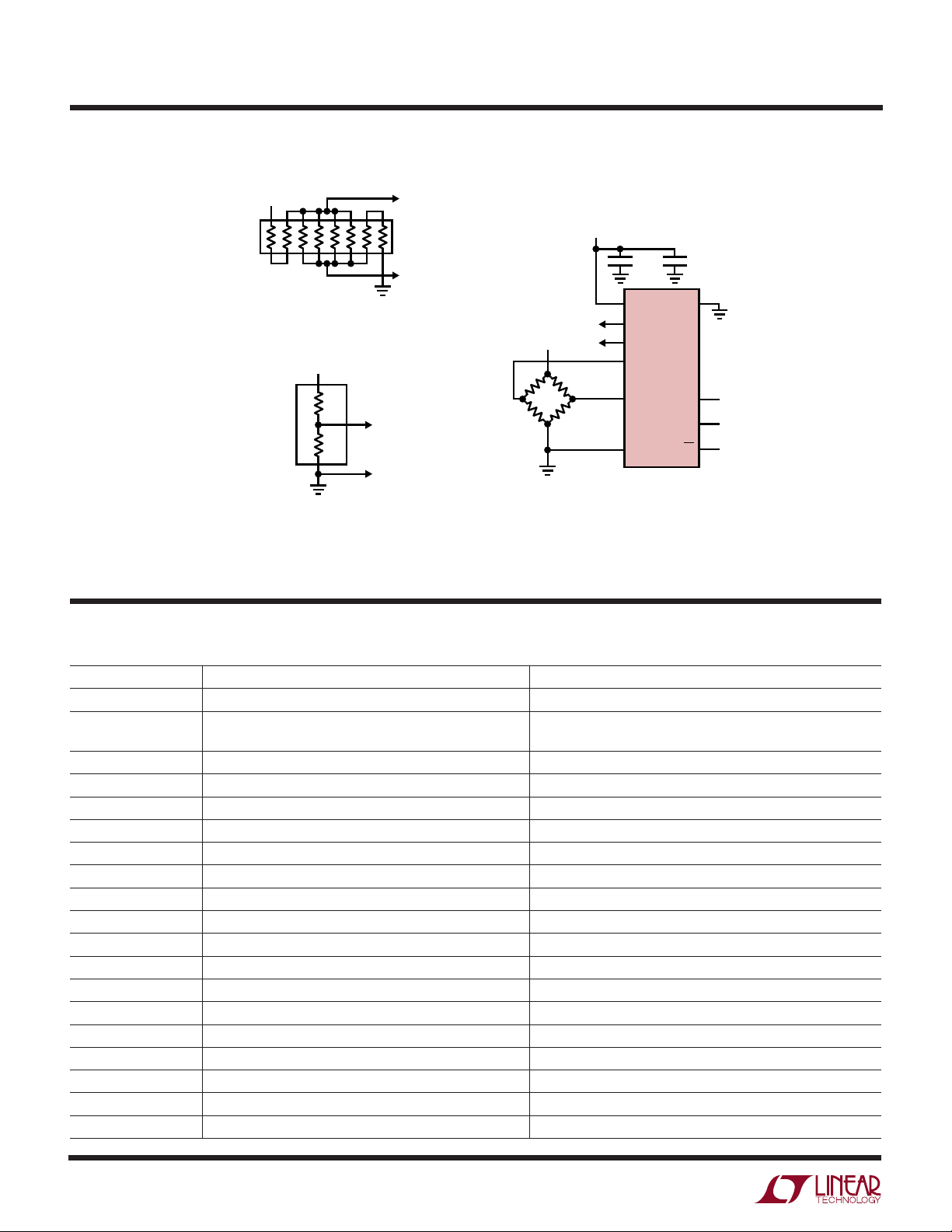
LTC2433-1
TYPICAL APPLICATIO
U
PANASONIC EXB-2HV202G
5V
8 × 2k
ARRAY
V
±147mV INPUT RANGE
VISHAY MPM1001/5002B
±49mV INPUT RANGE
Figure 30. Increased Resolution Bridge/Temperature Measurement
= 294mV
REF
4.5µV LSB
5V
V
= 95.04mV
REF
1.5µV LSB
50k
1k
REF
REF
REF
REF
+
–
+
–
HONEYWELL
FORCE SENSOR
FSL05N2C
500 GRAM
5V
0.1µF
110
V
CC
2
REF
5V
3
4
5
6
REF
+
IN
LTC2433-1
–
IN
GND
4.7µF
F
O
+
–
9
SCK
8
SDO
7
CS
24331 F30
RELATED PARTS
PART NUMBER DESCRIPTION COMMENTS
LT1019 Precision Bandgap Reference, 2.5V, 5V 3ppm/°C Drift, 0.05% Max
LTC1043 Dual Precision Instrumentation Switched Capacitor Precise Charge, Balanced Switching, Low Power
Building Block
LTC1050 Precision Chopper Stabilized Op Amp No External Components 5µV Offset, 1.6µV
LT1236A-5 Precision Bandgap Reference, 5V 0.05% Max, 5ppm/°C Drift
LT1461 Micropower Precision LDO Reference High Accuracy 0.04% Max, 3ppm/°C Max Drift
LTC2400 24-Bit, No Latency ∆Σ ADC in SO-8 0.3ppm Noise, 4ppm INL, 10ppm Total Unadjusted Error, 200µA
LTC2401/LTC2402 1-/2-Channel, 24-Bit, No Latency ∆Σ ADC in MSOP 0.6ppm Noise, 4ppm INL, 10ppm Total Unadjusted Error, 200µA
LTC2404/LTC2408 4-/8-Channel, 24-Bit, No Latency ∆Σ ADC 0.3ppm Noise, 4ppm INL, 10ppm Total Unadjusted Error, 200µA
LTC2410 24-Bit, Fully Differential, No Latency ∆Σ ADC 0.16ppm Noise, 2ppm INL, 3ppm Total Unadjusted Error, 200µA
LTC2411 24-Bit, No Latency ∆Σ ADC in MSOP 1.45µV
Noise, 2ppm INL, Pin Compatible with LTC2433-1
RMS
LTC2412 2-Channel, 24-Bit, Pin Compatible with LTC2436-1 800nV Noise, 2ppm INL, 3ppm TUE, 200µA
LTC2413 24-Bit, No Latency ∆Σ ADC Simultaneous 50Hz/60Hz Rejection, 800nV
LTC2414/LTC2418 8-/16-Channel, 24-Bit No Latency ∆Σ ADC 0.2ppm Noise, 2ppm INL, 3ppm Total Unadjusted Error, 200µA
LTC2415 24-Bit, No Latency ∆Σ ADC with 15Hz Output Rate Pin Compatible with the LTC2410
LTC2420 20-Bit, No Latency ∆Σ ADC in SO-8 1.2ppm Noise, 8ppm INL, Pin Compatible with LTC2400
LTC2424/LTC2428 4-/8-Channel, 20-Bit, No Latency ∆Σ ADCs 1.2ppm Noise, 8ppm INL, Pin Compatible with LTC2404/LTC2408
LTC2431 20-Bit, Differential No Latency ∆Σ ADC Pin Compatible with LTC2433-1
LTC2436-1 Low Cost 16-Bit ∆Σ ADC 800nV
Noise 2-Channel Ping-Pong
RMS
LTC2440 High Speed, Low Noise 24-Bit ADC 4kHz Output Rate, 200µV Noise, 24.6 ENOBs
LT/TP 0104 1K REV A • PRINTED IN USA
LINEAR TECHNOLOGY CORPORATION 2003
28
Linear Technology Corporation
1630 McCarthy Blvd., Milpitas, CA 95035-7417
(408) 432-1900 ● FAX: (408) 434-0507
●
www.linear.com
P-P
RMS
Noise
Noise
24331fa
 Loading...