

Page 1
No Latency ∆Σ
Final Electrical Specifications
LTC2420
20-Bit µPower
TM
ADC in SO-8
FEATURES
■
20-Bit ADC in SO-8 Package
■
8ppm INL, No Missing Codes at 20 Bits
■
4ppm Full-Scale Error
■
0.5ppm Offset
■
1.2ppm Noise
■
Digital Filter Settles in a Single Cycle. Each
Conversion Is Accurate, Even After an Input Step.
■
Internal Oscillator—No External Components
Required
■
Fast Mode: 16-Bit Noise, 12 Bits TUE at 100sps
■
110dB Min, 50Hz/60Hz Notch Filter
■
Reference Input Voltage: 0.1V to V
■
Live Zero—Extended Input Range Accommodates
CC
12.5% Overrange and Underrange
■
Single Supply 2.7V to 5.5V Operation
■
Low Supply Current (200µA) and Auto Shutdown
■
Pin Compatible with 24-Bit LTC2400
U
APPLICATIO S
■
Weight Scales
■
Direct Temperature Measurement
■
Gas Analyzers
■
Strain-Gage Transducers
■
Instrumentation
■
Data Acquisition
■
Industrial Process Control
■
4-Digit DVMs
U
January 2000
DESCRIPTIO
The LTC®2420 is a micropower 20-bit A/D converter with
an integrated oscillator, 8ppm INL and 1.2ppm RMS
noise that operates from 2.7V to 5.5V. It uses delta-sigma
technology and provides a digital filter that settles in a
single cycle for multiplexed applications. Through a single
pin, the LTC2420 can be configured for better than 110dB
rejection at 50Hz or 60Hz ±2%, or it can be driven by an
external oscillator for a user-defined rejection frequency
in the range 1Hz to 800Hz. The internal oscillator requires
no external frequency setting components.
The converter accepts any external reference voltage from
0.1V to VCC. With its extended input conversion range of
–12.5% V
resolves the offset and overrange problems of preceding
sensors or signal conditioning circuits.
The LTC2420 communicates through a flexible 3-wire
digital interface which is compatible with SPI and
MICROWIRETM protocols.
, LTC and LT are registered trademarks of Linear Technology Corporation.
No Latency ∆Σ is a trademark of Linear Technology Corporation.
MICROWIRE is a trademark of National Semiconductor Corporation.
to 112.5% V
REF
, the LTC2420 smoothly
REF
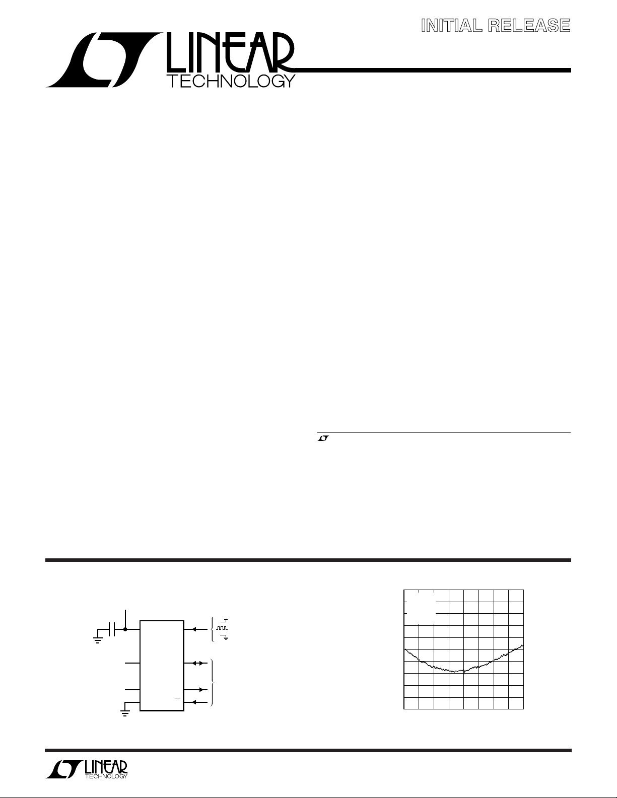
TYPICAL APPLICATIO
2.7V TO 5.5V
1µF
1
REFERENCE
VOLTAGE
0.1V TO V
ANALOG
INPUT RANGE
TO 1.12V
–0.12V
REF
REF
2
CC
3
4
V
CC
LTC2420
V
SCK
REF
SDO
V
IN
GND CS
U
Total Unadjusted Error vs Output Code
10
VCC = 5V
8
= 5V
V
REF
= 25°C
T
V
CC
8
F
O
7
6
5
Information furnished by Linear Technology Corporation is believed to be accurate and reliable.
However, no responsibility is assumed for its use. Linear Technology Corporation makes no representation that the interconnection of its circuits as described herein will not infringe on existing patent rights.
= INTERNAL OSC/50Hz REJECTION
= EXTERNAL CLOCK SOURCE
= INTERNAL OSC/60Hz REJECTION
3-WIRE
SPI INTERFACE
2420 TA01
A
6
= LOW
F
O
4
2
0
–2
–4
–6
TOTAL UNADJUSTED ERROR (ppm)
–8
–10
0 524,288 1,048,575
OUTPUT CODE (DECIMAL)
2420 TA02
1
Page 2
LTC2420
WW
W
ABSOLUTE MAXIMUM RATINGS
U
UUW
PACKAGE/ORDER INFORMATION
(Notes 1, 2)
Supply Voltage (VCC) to GND.......................– 0.3V to 7V
Analog Input Voltage to GND ....... –0.3V to (VCC + 0.3V)
Reference Input Voltage to GND .. –0.3V to (VCC + 0.3V)
Digital Input Voltage to GND........ –0.3V to (VCC + 0.3V)
Digital Output Voltage to GND ..... –0.3V to (VCC + 0.3V)
Operating Temperature Range
LTC2420C ............................................... 0°C to 70°C
LTC2420I............................................ –40°C to 85°C
Storage Temperature Range ................. –65°C to 150°C
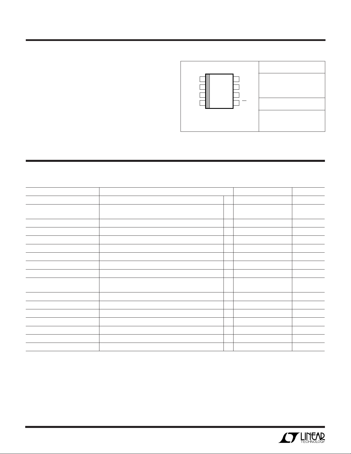
TOP VIEW
V
1
CC
V
2
REF
V
3
IN
GND
4
S8 PACKAGE
8-LEAD PLASTIC SO
T
= 125°C, θJA = 130°C/W
JMAX
Consult factory for Military grade parts.
8
F
O
SCK
7
SDO
6
CS
5
ORDER PART NUMBER
LTC2420CS8
LTC2420IS8
S8 PART MARKING
2420
2420I
Lead Temperature (Soldering, 10 sec)..................300°C
U
CONVERTER CHARACTERISTICS
temperature range, otherwise specifications are at TA = 25°C. (Notes 3, 4)
PARAMETER CONDITIONS MIN TYP MAX UNITS
Resolution (No Missing Codes) 0.1V ≤ V
Integral Nonlinearity V
Integral Nonlinearity (Fast Mode) V
Offset Error 2.5V ≤ V
Offset Error (Fast Mode) 2.5V < V
Offset Error Drift 2.5V ≤ V
Full-Scale Error 2.5V ≤ V
Full-Scale Error (Fast Mode) 2.5V < V
Full-Scale Error Drift 2.5V ≤ V
Total Unadjusted Error V
Output Noise VIN = 0V (Note 13) 6 µV
Output Noise (Fast Mode) V
Normal Mode Rejection 60Hz ±2% (Note 7) ● 110 130 dB
Normal Mode Rejection 50Hz ±2% (Note 8) ● 110 130 dB
Power Supply Rejection, DC V
Power Supply Rejection, 60Hz ±2% V
Power Supply Rejection, 50Hz ±2% V
REF
V
REF
REF
REF
V
REF
REF
REF
REF
REF
≤ VCC, (Note 5) ● 20 Bits
REF
= 2.5V (Note 6) ● 4 10 ppm of V
= 5V (Note 6) ● 8 20 ppm of V
= 5V, V
= 2.5V 8 ppm of V
= 5V 16 ppm of V
= 5V, 100 Samples/Second, fO = 2.048MHz 20 µV
= 2.5V, VIN = 0V 100 dB
= 2.5V, VIN = 0V, (Note 7) 110 dB
= 2.5V, VIN = 0V, (Note 8) 110 dB
= 2.5V, 100 Samples/Second, fO = 2.048MHz ● 40 250 ppm of V
REF
≤ V
REF
CC
< 5V, 100 Samples/Second, fO = 2.048MHz 3 ppm of V
REF
≤ V
REF
CC
≤ V
REF
CC
< 5V, 100 Samples/Second, fO = 2.048MHz 10 ppm of V
REF
≤ V
REF
CC
The ● denotes specifications which apply over the full operating
● 0.5 10 ppm of V
0.04 ppm of V
● 4 10 ppm of V
0.04 ppm of V
REF
REF
REF
REF
REF
REF
REF
/°C
REF
REF
/°C
REF
REF
RMS
RMS
2
Page 3
LTC2420
UU
U
A ALOG I PUT A D REFERE CE
U
The ● denotes specifications which apply over the full operating
temperature range, otherwise specifications are at TA = 25°C. (Note 3)
SYMBOL PARAMETER CONDITIONS MIN TYP MAX UNITS
V
IN
V
REF
C
S(IN)
C
S(REF)
I
IN(LEAK)
I
REF(LEAK)
Input Voltage Range (Note 14) ● –0.125 • V
Reference Voltage Range ● 0.1 V
Input Sampling Capacitance 1 pF
Reference Sampling Capacitance 1.5 pF
Input Leakage Current CS = V
Reference Leakage Current V
= 2.5V, CS = V
REF
CC
CC
● –100 1 100 nA
● –100 1 100 nA
REF
1.125 • V
CC
REF
UU
DIGITAL I PUTS A D DIGITAL OUTPUTS
operating temperature range, otherwise specifications are at TA = 25°C. (Note 3)
SYMBOL PARAMETER CONDITIONS MIN TYP MAX UNITS
V
IH
V
IL
V
IH
V
IL
I
IN
I
IN
C
IN
C
IN
V
OH
V
OL
V
OH
V
OL
I
OZ
High Level Input Voltage 2.7V ≤ VCC ≤ 5.5V ● 2.5 V
CS, F
O
Low Level Input Voltage 4.5V ≤ VCC ≤ 5.5V ● 0.8 V
CS, F
O
High Level Input Voltage 2.7V ≤ VCC ≤ 5.5V (Note 9) ● 2.5 V
SCK 2.7V ≤ V
Low Level Input Voltage 4.5V ≤ VCC ≤ 5.5V (Note 9) ● 0.8 V
SCK 2.7V ≤ V
Digital Input Current 0V ≤ VIN ≤ V
CS, F
O
Digital Input Current 0V ≤ VIN ≤ VCC (Note 9) ● –10 10 µA
SCK
Digital Input Capacitance 10 pF
CS, F
O
Digital Input Capacitance (Note 9) 10 pF
SCK
High Level Output Voltage IO = –800µA ● VCC – 0.5 V
SDO
Low Level Output Voltage IO = 1.6mA ● 0.4 V
SDO
High Level Output Voltage IO = –800µA (Note 10) ● VCC – 0.5 V
SCK
Low Level Output Voltage IO = 1.6mA (Note 10) ● 0.4 V
SCK
High-Z Output Leakage ● –10 10 µA
SDO
2.7V ≤ VCC ≤ 3.3V 2.0 V
2.7V ≤ VCC ≤ 5.5V 0.6 V
The ● denotes specifications which apply over the full
≤ 3.3V (Note 9) 2.0 V
CC
≤ 5.5V (Note 9) 0.6 V
CC
CC
● –10 10 µA
V
V
WU
POWER REQUIRE E TS
The ● denotes specifications which apply over the full operating temperature range,
otherwise specifications are at TA = 25°C. (Note 3)
SYMBOL PARAMETER CONDITIONS MIN TYP MAX UNITS
V
CC
I
CC
Supply Voltage ● 2.7 5.5 V
Supply Current
Conversion Mode CS = 0V (Note 12)
Sleep Mode CS = V
(Note 12) ● 20 30 µA
CC
● 200 300 µA
3
Page 4
LTC2420
UW
TI I G CHARACTERISTICS
range, otherwise specifications are at TA = 25°C. (Note 3)
SYMBOL PARAMETER CONDITIONS MIN TYP MAX UNITS
f
EOSC
t
HEO
t
LEO
t
CONV
f
ISCK
D
ISCK
f
ESCK
t
LESCK
t
HESCK
t
DOUT_ISCK
t
DOUT_ESCK
t
1
t2 CS ↑ to SDO High Z ● 0 150 ns
t3 CS ↓ to SCK ↓ (Note 10) ● 0 150 ns
t4 CS ↓ to SCK ↑ (Note 9) ● 50 ns
t
KQMAX
t
KQMIN
t
5
t
6
External Oscillator Frequency Range 20-Bit Effective Resolution ● 2.56 307.2 kHz
External Oscillator High Period ● 0.5 390 µs
External Oscillator Low Period ● 0.5 390 µs
Conversion Time FO = 0V ● 130.66 133.33 136 ms
Internal SCK Frequency Internal Oscillator (Note 10) 19.2 kHz
Internal SCK Duty Cycle (Note 10) 45 55 %
External SCK Frequency Range (Note 9) ● 2000 kHz
External SCK Low Period (Note 9) ● 250 ns
External SCK High Period (Note 9) ● 250 ns
Internal SCK 24-Bit Data Output Time Internal Oscillator (Notes 10, 12) ● 1.23 1.25 1.28 ms
External SCK 24-Bit Data Output Time (Note 9) ● 24/f
CS ↓ to SDO Low Z ● 0 150 ns
SCK ↓ to SDO Valid ● 200 ns
SDO Hold After SCK ↓ (Note 5) ● 15 ns
SCK Set-Up Before CS ↓ ● 50 ns
SCK Hold After CS ↓ ● 50 ns
The ● denotes specifications which apply over the full operating temperature
12-Bit Effective Resolution
= V
F
O
CC
External Oscillator (Note 11)
External Oscillator (Notes 10, 11) f
External Oscillator (Notes 10, 11)
● 2.56 2.048 MHz
● 156.80 160 163.20 ms
● 20480/f
● 192/f
(in kHz) ms
EOSC
/8 kHz
EOSC
(in kHz) ms
EOSC
(in kHz) ms
ESCK
Note 1: Absolute Maximum Ratings are those values beyond which the
life of the device may be impaired.
Note 2: All voltage values are with respect to GND.
Note 3: All voltages are with respect to GND. V
otherwise specified. R
SOURCE
= 0Ω.
= 2.7 to 5.5V unless
CC
Note 4: Internal Conversion Clock source with the FO pin tied
to GND or to V
= 153600Hz unless otherwise specified.
f
EOSC
or to external conversion clock source with
CC
Note 5: Guaranteed by design, not subject to test.
Note 6: Integral nonlinearity is defined as the deviation of a code from
a straight line passing through the actual endpoints of the transfer
curve. The deviation is measured from the center of the quantization
band.
Note 7: FO = 0V (internal oscillator) or f
= 153600Hz ±2%
EOSC
(external oscillator).
Note 8: F
= VCC (internal oscillator) or f
O
= 128000Hz ±2%
EOSC
(external oscillator).
Note 9: The converter is in external SCK mode of operation such that
the SCK pin is used as digital input. The frequency of the clock signal
driving SCK during the data output is f
and is expressed in kHz.
ESCK
Note 10: The converter is in internal SCK mode of operation such that
the SCK pin is used as digital output. In this mode of operation the
SCK pin has a total equivalent load capacitance C
LOAD
= 20pF.
Note 11: The external oscillator is connected to the FO pin. The external
oscillator frequency, f
, is expressed in kHz.
EOSC
Note 12: The converter uses the internal oscillator.
= 0V or FO = VCC.
F
O
Note 13: The output noise includes the contribution of the internal
calibration operations.
Note 14: For reference voltage values V
of –0.125 • V
to 1.125 • V
REF
is limited by the absolute maximum
REF
rating of the Analog Input Voltage pin (Pin 3). For 2.5V < V
0.267V + 0.89 • V
For 0.267V + 0.89 • V
to V
+ 0.3V.
CC
the input voltage range is –0.3V to 1.125 • V
CC
< V
CC
≤ VCC the input voltage range is –0.3V
REF
> 2.5V the extended input
REF
REF
≤
.
REF
4
Page 5

LTC2420
U
UU
PIN FUNCTIONS
VCC (Pin 1): Positive Supply Voltage. Bypass to GND
(Pin␣ 4) with a 10µF tantalum capacitor in parallel with
0.1µF ceramic capacitor as close to the part as possible.
V
(Pin 2): Reference Input. The reference voltage range
REF
is 0.1V to VCC.
VIN (Pin 3): Analog Input. The input voltage range is
–0.125 • V
voltage range may be limited by the pin absolute maximum rating of –0.3V to VCC + 0.3V.
GND (Pin 4): Ground. Shared pin for analog ground,
digital ground, reference ground and signal ground. Should
be connected directly to a ground plane through a minimum length trace or it should be the single-point-ground
in a single point grounding system.
CS (Pin 5): Active LOW Digital Input. A LOW on this pin
enables the SDO digital output and wakes up the ADC.
Following each conversion, the ADC automatically enters
the Sleep mode and remains in this low power state as
long as CS is HIGH. A LOW on CS wakes up the ADC. A
LOW-to-HIGH transition on this pin disables the SDO
digital output. A LOW-to-HIGH transition on CS during the
Data Output transfer aborts the data transfer and starts a
new conversion.
to 1.125 • V
REF
REF
. For V
> 2.5V the input
REF
SDO (Pin 6): Three-State Digital Output. During the data
output period this pin is used for serial data output. When
the chip select CS is HIGH (CS = VCC), the SDO pin is in a
high impedance state. During the Conversion and Sleep
periods, this pin can be used as a conversion status output. The conversion status can be observed by pulling CS
LOW.
SCK (Pin 7): Bidirectional Digital Clock Pin. In Internal
Serial Clock Operation mode, SCK is used as digital output
for the internal serial interface clock during the data output
period. In External Serial Clock Operation mode, SCK is
used as digital input for the external serial interface. A
weak internal pull-up is automatically activated in Internal
Serial Clock Operation mode. The Serial Clock mode is
determined by the level applied to SCK at power up and the
falling edge of CS.
FO (Pin 8): Frequency Control Pin. Digital input that
controls the ADC’s notch frequencies and conversion
time. When the FO pin is connected to VCC (FO = VCC), the
converter uses its internal oscillator and the digital filter’s
first null is located at 50Hz. When the FO pin is connected
to GND (FO = OV) the converter uses its internal oscillator
and the digital filter first null is located at 60Hz. When F
is driven by an external clock signal with a frequency f
the converter uses this signal as its clock and the digital
filter first null is located at a frequency f
EOSC
/2560.
EOSC
O
,
U
WUU
APPLICATIO S I FOR ATIO
The LTC2420 is pin compatible with the LTC2400. The two
devices are designed to allow the user to incorporate
either device in the same design with no modifications.
While the LTC2420 output word length is 24 bits (as
opposed to the 32-bit output of the LTC2400), its output
clock timing can be identical to the LTC2400. As shown in
Figure 1, the LTC2420 data output is concluded on the
falling edge of the 24th serial clock (SCK). In order to
maintain drop-in compatibility with the LTC2400, it is
possible to clock the LTC2420 with an additional 8 serial
clock pulses. This results in 8 additional output bits which
are always logic HIGH.
Output Data Format
The LTC2420 serial output data stream is 24 bits long. The
first 4 bits represent status information indicating the
sign, input range and conversion state. The next 20 bits are
the conversion result, MSB first.
Bit 23 (first output bit) is the end of conversion (EOC)
indicator. This bit is available at the SDO pin during the
conversion and sleep states whenever the CS pin is LOW.
This bit is HIGH during the conversion and goes LOW
when the conversion is complete.
Bit 22 (second output bit) is a dummy bit (DMY) and is
always LOW.
5
Page 6

LTC2420
U
WUU
APPLICATIO S I FOR ATIO
CS
8 8 8 8 (OPTIONAL)
SCK
SDO
EOC = 1
CONVERSION SLEEP
Bit 21 (third output bit) is the conversion result sign indicator (SIG). If VIN is >0, this bit is HIGH. If VIN is <0, this
bit is LOW. The sign bit changes state during the zero code.
Bit 20 (forth output bit) is the extended input range (EXR)
indicator. If the input is within the normal input range
0␣ ≤␣VIN ≤ V
normal input range, VIN > V
, this bit is LOW. If the input is outside the
REF
or VIN < 0, this bit is HIGH.
REF
The function of these bits is summarized in Table 1.
Table 1. LTC2420 Status Bits
Bit 23 Bit 22 Bit 21 Bit 20
Input Range EOC DMY SIG EXR
VIN > V
REF
0 < VIN ≤ V
VIN = 0+/0
VIN < 0 0 001
REF
–
0 011
0 010
0 0 1/0 0
EOC = 0
4 STATUS BITS 20 DATA BITS
Figure 1. LTC2420 Compatible Timing with the LTC2400
edge of SCK. Bit 22 is shifted out of the device on the first
falling edge of SCK. The final data bit (Bit 0) is shifted out
on the falling edge of the 23rd SCK and may be latched on
the rising edge of the 24th SCK pulse. On the falling edge
of the 24th SCK pulse, SDO goes HIGH indicating a new
conversion cycle has been initiated. This bit serves as EOC
(Bit 23) for the next conversion cycle. Table 2 summarizes
the output data format.
As long as the voltage on the VIN pin is maintained within
the –0.3V to (VCC + 0.3V) absolute maximum operating
range, a conversion result is generated for any input value
from –0.125 • V
greater than 1.125 • V
to the value corresponding to 1.125 • V
voltages below –0.125 • V
clamped to the value corresponding to –0.125 • V
DATA OUT
CONVERSION
EOC = 1
LAST 8 BITS ALWAYS 1
to 1.125 • V
REF
, the conversion result is clamped
REF
DATA OUTPUT
REF.
, the conversion result is
REF
2420 F01
For input voltages
. For input
REF
REF
.
Bit 19 (fifth output bit) is the most significant bit (MSB).
Bits 19-0 are the 20-bit conversion result MSB first.
Bit 0 is the least significant bit (LSB).
Data is shifted out of the SDO pin under control of the serial
clock (SCK), see Figure 2. Whenever CS is HIGH, SDO
remains high impedance and any SCK clock pulses are
ignored by the internal data out shift register.
In order to shift the conversion result out of the device, CS
must first be driven LOW. EOC is seen at the SDO pin of the
device once CS is pulled LOW. EOC changes real time from
HIGH to LOW at the completion of a conversion. This
signal may be used as an interrupt for an external microcontroller. Bit 23 (EOC) can be captured on the first rising
6
Operation at Higher Data Output Rates
The LTC2420 typically operates with an internal oscillator
of 153.6kHz. This corresponds to a notch frequency of
60Hz and an output rate of 7.5 samples/second. The
internal oscillator is enabled if the FO pin is logic LOW
(logic HIGH for a 50Hz notch). It is possible to drive the F
O
pin with an external oscillator for higher data output rates.
As shown in Figure 3, an external clock of 2.048MHz
applied to the FO pin results in a notch frequency of 800Hz
with a data output rate of 100 samples/second.
Figure 4 shows the total unadjusted error (Offset Error +
Full-Scale Error + INL + DNL) as a function of the output
data rate with a 5V reference. The relationship between the
Page 7

LTC2420
U
WUU
APPLICATIO S I FOR ATIO
CS
BIT 0BIT 19 BIT 4
LSB
20
2420 F02
SDO
SCK
BIT 23
EOC
Hi-Z
1 2 3 4 5 192024
SLEEP DATA OUTPUT CONVERSION
BIT 20BIT 21BIT 22
MSBEXTSIG“0”
Figure 2. Output Data Timing
Table 2. LTC2420 Output Data Format
Bit 23 Bit 22 Bit 21 Bit 20 Bit 19 Bit 18 Bit 17 Bit 16 Bit 15 … Bit 0
Input Voltage EOC DMY SIG EXR MSB LSB
VIN > 9/8 • V
9/8 • V
V
REF
V
REF
3/4V
3/4V
1/2V
1/2V
1/4V
1/4V
0+/0
REF
REF
+ 1LSB 0 01100 0 00...0
+ 1LSB 0 01011 0 00...0
REF
REF
+ 1LSB 0 01010 0 00...0
REF
REF
+ 1LSB 0 01001 0 00...0
REF
REF
–
–1LSB 0 0 0111 1 11...1
–1/8 • V
REF
VIN < –1/8 • V
REF
*The sign bit changes state during the 0 code.
0 01100 0 11...1
0 01100 0 11...1
0 01011 1 11...1
0 01010 1 11...1
0 01001 1 11...1
0 01000 1 11...1
0 01/0*000 0 00...0
0 00111 1 00...0
0 00111 1 00...0
800Hz NOTCH (100 SAMPLES/SECOND)
60Hz NOTCH (7.5 SAMPLES/SECOND)
LTC2420
1
V
CC
2
V
REF
3
V
IN
4
GND
8
F
O
7
SCK
6
SDO
5
CS
INTERNAL 153.6kHz OSCILLATOR
EXTERNAL 2.048MHz CLOCK SOURCE
2420 F03
Figure 3. Selectable 100 Samples/Second Turbo Mode
256
224
192
160
128
TOTAL UNADJUSTED ERROR (ppm)
= 5V
V
REF
96
64
32
0
0
50 100
OUTPUT RATE (SAMPLES/SEC)
12 BITS
13 BITS
14 BITS
16 BITS
2420 F04
Figure 4. Total Error vs Output Rate (V
150
REF
= 5V)
7
Page 8

LTC2420
U
WUU
APPLICATIO S I FOR ATIO
output data rate (ODR) and the frequency applied to the F
pin (FO) is:
ODR = FO/20480
For output data rates up to 50 samples/second, the total
unadjusted error (TUE) is better than 16 bits, and better
than 12 bits at 100 samples/second. As shown in Figure 5,
for output data rates of 100 samples/second, the TUE is
better than 15 bits for V
below 2.5V. Figure 6 shows an
REF
unaveraged total unadjusted error for the LTC2420 operating at 100 samples/second with V
= 2.5V. Figure 7
REF
shows the same device operating with a 5V reference and
an output data rate of 7.5 samples/second.
256
OUTPUT RATE = 100sps
224
192
160
128
96
64
TOTAL UNADJUSTED ERROR (ppm)
32
0
1.5
1.0
2.0
REFERENCE VOLTAGE (V)
2.5
3.0
3.5
12 BITS
13 BITS
14 BITS
15 BITS
4.0
4.5
2420 F05
5.0
O
At 100 samples/second, the LTC2420 can be used to
capture transient data. This is useful for monitoring settling or auto gain ranging in a system. The LTC2420 can
monitor signals at an output rate of 100 samples/second.
After acquiring 100 samples/second data the FO pin may
be driven LOW enabling 60Hz rejection to 110dB and the
highest possible DC accuracy. The no latency architecture
of the LTC2420 allows consecutive readings (one at 100
samples/second the next at 7.5 samples/second) without
interaction between the two readings.
10
5
0
–5
–10
–15
–20
–25
–30
TOTAL UNADJUSTED ERROR (ppm)
–35
–40
0
INPUT VOLTAGE (V)
VCC = 5V
= 2.5V
V
REF
2.5
2420 F06
Figure 5. Total Error vs V
8
(Output Rate = 100sps)
REF
6
4
2
0
–2
–4
–6
TOTAL UNADJUSTED ERROR (ppm)
–8
–10
0
INPUT VOLTAGE (V)
VCC = 5V
= 5V
V
REF
2420 F07
Figure 7. Total Unadjusted Error at 7.5 Samples/Second
(No Averaging)
Figure 6. Total Unadjusted Error at
100 Samples/Second (No Averaging)
5
Page 9

LTC2420
U
WUU
APPLICATIO S I FOR ATIO
As shown in Figure 8, the LTC2420 can capture transient
data with 90dB of dynamic range (with a 300mV
signal at 2Hz). The exceptional DC performance of the
LTC2420 enables signals to be digitized independent of a
0.20
0.15
0.10
0.05
–0.05
–0.10
–0.15
ADC OUTPUT (NORMALIZED TO VOLTS)
–0.20
500ms
0
TIME
8a. Digitized Waveform
2.20
V
= 300mV
IN
2.15
2.10
2.05
2.00
1.95
1.90
1.85
ADC OUTPUT (NORMALIZED TO VOLTS)
1.80
P-P
+ 2V DC
TIME
= 2Hz
f
IN
2420 F08a
Figure 8. Transient Signal Acquisiton
2420 F09a
P-P
input
large DC offset. Figures 9a and 9b show the dynamic
performance with a 15Hz signal superimposed on a 2V DC
level. The same signal with no DC level is shown in Figures
9c and 9d.
0
–20
–40
–60
MAGNITUDE (dB)
–80
–100
–120
0
–20
–40
–60
MAGNITUDE (dB)
–80
–100
–120
FREQUENCY (Hz)
8b. Output FFT
FREQUENCY (Hz)
2Hz
100sps
0V OFFSET
2420 F08b
15Hz
100sps
2V OFFSET
2420 F09b
9a. Digitized Waveform with 2V DC Offset 9b. FFT Waveform with 2V DC Offset
0.20
V
= 300mV
IN
0.15
0.10
0.05
0.00
–0.05
–0.10
–0.15
ADC OUTPUT (NORMALIZED TO VOLTS)
–0.20
P-P
+ 0V DC
TIME
2420 F09c
9c. Digitized Waveform with No Offset
0
–20
–40
–60
MAGNITUDE (dB)
–80
–100
–120
FREQUENCY (Hz)
9d. FFT Waveform with No Offset
15Hz
100sps
0V OFFSET
2420 F09d
Figure 9. Using the LTC2420’s High Accuracy Wide Dynamic Range to Digitize
a 300mV
15Hz Waveform with a Large DC Offset (VCC = 5V, V
P-P
REF
= 5V)
9
Page 10

LTC2420
U
WUU
APPLICATIO S I FOR ATIO
Single-Chip Instrumentation Amplifier
for the LTC2420
The circuit in Figure 10 is a simple solution for processing
differential signals in pressure transducer, weigh scale or
strain gauge applications that can operate on a supply
voltage range of ±5V to ±15V. The circuit uses an LT®1920
single-chip instrumentation amplifier to perform a differential to single-ended conversion. The amplifier’s output
voltage is applied to the LTC2420’s input and converted to
a digital value with an overall accuracy exceeding 17 bits
(0.0008%). Key circuit performance results are shown in
Table 3.
The practical gain range for this topology as shown is from
5 to 100 because the LTC2420’s wide dynamic range
makes gains below 5 virtually unnecessary, whereas gain
up to 100 significantly reduce the input referred noise.
The optional passive RC lowpass filter between the
amplifier’s output and the LTC2420’s input attenuates
high frequency noise and its effects. Typically, the filter
reduces the magnitude of averaged noise by 30% and
improves resolution by 0.5 bit without compromising
linearity. Resistor R2 performs two functions: it isolates
C1 from the LTC2420’s input and limits the LTC2420’s
input current should its input voltage drop below –300mV
or swing above VCC + 300mV.
The LT1920 is the choice for applications where low cost
is important. For applications where more precision is
required, the LT1167 is a pin-to-pin alternative choice with
a lower offset voltage, lower input bias current and higher
gain accuracy than the LT1920. The LT1920’s maximum
total input-referred offset (V
100. At the same gain, the LT1167’s V
) is 135µV for a gain of
OST
is 63µV. At gains
OST
of 10 or 100, the LT1920’s maximum gain error is 0.3%
and its maximum gain nonlinearity is 30ppm. At the same
gains, the LT1167’s maximum gain error is 0.1% and its
maximum gain nonlinearity is 15ppm. Table 4 summarizes the performance of Figure 10’s circuit using the
LT1167.
DIFFERENTIAL
INPUT
Figure 10. The LT1920 is a Simple Solution That Converts a Differential Input
to a Ground Referred Single-Ended Signal for the LTC2420
RG**
V
REFIN
+
V
S
2
+
V
IN
R
G
1
LT1920
8
R
G
–
V
IN
3
*OPTIONAL—SEE TEXT
**R
†
USE SHORT LEAD LENGTHS
0.1µF
7
4
–
V
S
= 49.4k/(AV – 1): USE 5.49k FOR AV = 10; 499Ω FOR AV = 100
G
R1*
47Ω
6
0.1µF
†
††
2
R2*
10k
3
C1*
1µF
SINGLE POINT
“STAR” GROUND
V
V
IN
1
V
CC
REF
LTC2420
GND
48
0.1µF5V
5
CHIP SELECT
CS
6
SDO
SCK
F
O
SERIAL DATA OUT
7
SERIAL CLOCK
2429 F10
10
Page 11

LTC2420
U
WUU
APPLICATIO S I FOR ATIO
Table 3. Typical Performance of the LTC2420 ADC When Used with the
LT1920 Instrumentation Amplifiers in Figure 9’s Differential Digitizing Circuit
VS = ±5V VS = ±15V
PARAMETER AV = 10 AV = 100 AV = 10 AV = 100 TOTAL (UNITS)
Differential Input Voltage Range – 30 to 400 – 3 to 40 –30 to 500 –3 to 50 mV
Zero Error –160 –2650 – 213 –2625 µV
Maximum Input Current 2.0 nA
Nonlinearity ±8.2 ±7.4 ±6.5 ±6.1 ppm
Noise (Without Averaging) 1.8* 0.25* 1.5* 0.27* µV
Noise (Averaged 64 Readings) 0.2* 0.03* 0.19* 0.03* µV
Resolution (with Averaged Readings) 21 20.6 21.3 20.5 Bits
Overall Accuracy (Uncalibrated) 17.2 17.3 17.5 18.2 Bits
Common Mode Rejection Ratio ≥120 dB
Common Mode Range 2/–1.5** 2.2/–1.7** 11.5/–11** 11.7/–11.2** V
*Input referred noise for the respective gain. **Typical values based on single lab tested sample of each amplifier.
Table 4. Typical Performance of the LTC2420 ADC When Used with the
LT1167 Instrumentation Amplifiers in Figure 9’s Differential Digitizing Circuit
VS = ±5V VS = ±15V
PARAMETER AV = 10 AV = 100 AV = 10 AV = 100 TOTAL (UNITS)
Differential Input Voltage Range – 30 to 400 – 3 to 40 –30 to 500 –3 to 50 mV
Zero Error –94 –1590 –110 – 1470 µV
Maximum Input Current 0.5 nA
Nonlinearity ±4.1 ±4.4 ±4.1 ±3.7 ppm
Noise (Without Averaging) 1.4* 0.19* 1.5* 0.18* µV
Noise (Averaged 64 Readings) 0.18* 0.02* 0.19* 0.02* µV
Resolution (with Averaged Readings) 21.4 21.0 21.3 21.1 Bits
Overall Accuracy (Uncalibrated) 18.2 18.1 18.2 19.4 Bits
Common Mode Rejection Ratio ≥120 dB
Common Mode Range 2/–1.5** 2.2/–1.7** 11.5/–11** 11.7/–11.2** V
*Input referred noise for the respective gain. **Typical values based on single lab tested sample of each amplifier.
RMS
RMS
RMS
RMS
11
Page 12

LTC2420
UU
W
PACKAGE I FOR ATIO
0.010 – 0.020
(0.254 – 0.508)
0.008 – 0.010
(0.203 – 0.254)
×
Dimensions in inches (millimeters) unless otherwise noted.
S8 Package
8-Lead Plastic Small Outline (Narrow 0.150)
(LTC DWG # 05-08-1610)
0.189 – 0.197*
(4.801 – 5.004)
45
7
8
0.228 – 0.244
(5.791 – 6.197)
1
2
°
0°– 8° TYP
0.053 – 0.069
(1.346 – 1.752)
5
6
0.150 – 0.157**
3
4
(3.810 – 3.988)
0.004 – 0.010
(0.101 – 0.254)
0.016 – 0.050
(0.406 – 1.270)
*
DIMENSION DOES NOT INCLUDE MOLD FLASH. MOLD FLASH
SHALL NOT EXCEED 0.006" (0.152mm) PER SIDE
**
DIMENSION DOES NOT INCLUDE INTERLEAD FLASH. INTERLEAD
FLASH SHALL NOT EXCEED 0.010" (0.254mm) PER SIDE
0.014 – 0.019
(0.355 – 0.483)
TYP
0.050
(1.270)
BSC
SO8 1298
RELATED PARTS
PART NUMBER DESCRIPTION COMMENTS
LT1019 Precision Bandgap Reference, 2.5V, 5V 3ppm/°C Drift, 0.05% Max
LT1025 Micropower Thermocouple Cold Junction Compensator 0.5°C Initial Accuracy, 80µA Supply Current
LTC1043 Dual Precision Instrumentation Switched Capacitor Precise Charge, Balanced Switching, Low Power
Building Block
LTC1050 Precision Chopper Stabilized Op Amp No External Components 5µV Offset, 1.6µV
LT1236A-5 Precision Bandgap Reference, 5V 0.05% Max, 5ppm/°C Drift
LTC1391 8-Channel Multiplexer Low RON: 45Ω, Low Charge Injection, Serial Interface
LT1460 Micropower Series Reference 0.075% Max, 10ppm/°C Max Drift, 2.5V, 5V and 10V Versions,
MSOP, PDIP, SO-8, SOT-23 and TO-92 Packages
LTC2400 24-Bit µPower, No Latency ∆Σ ADC in SO-8 4ppm INL, 10ppm Total Unadjusted Error, 200µA
LTC2408 8-Channel, 24-Bit No Latency ∆Σ ADC 4ppm INL, 10ppm Total Unadjusted Error, 200µA
P-P
Noise
12
Linear Technology Corporation
1630 McCarthy Blvd., Milpitas, CA 95035-7417
(408) 432-1900 ● FAX: (408) 434-0507
●
www.linear-tech.com
2420i LT/TP 0100 4K • PRINTED IN USA
LINEAR TECHNOLOGY CORPORATION 2000
 Loading...