

Page 1
FEATURES
LTC2404/LTC2408
4-/8-Channel 24-Bit µPower
TM
No Latency ∆Σ
ADCs
U
DESCRIPTIO
■
Pin Compatible 4-/8-Channel 24-Bit ADCs
■
Single Conversion Digital Filter Settling Time
Simplifies Multiplexing
■
4ppm INL, No Missing Codes
■
4ppm Full-Scale Error
■
0.5ppm Offset
■
0.3ppm Noise
■
Internal Oscillator—No External Components
Required
■
110dB Min, 50Hz/60Hz Notch Filter
■
Reference Input Voltage: 0.1V to V
■
Live Zero—Extended Input Range Accommodates
CC
12.5% Overrange and Underrange
■
Single Supply 2.7V to 5.5V Operation
■
Low Supply Current (200µA) and Auto Shutdown
U
APPLICATIO S
■
Weight Scales
■
Direct Temperature Measurement
■
Gas Analyzers
■
Strain-Gage Transducers
■
Instrumentation
■
Data Acquisition
■
Industrial Process Control
■
6-Digit DVMs
The LTC®2404/LTC2408 are 4-/8-channel 2.7V to 5.5V
micropower 24-bit A/D converters with an integrated
oscillator, 4ppm INL and 0.3ppm RMS noise. They use
delta-sigma technology and provide single cycle digital
filter settling time (no latency delay) for multiplexed
applications. The first conversion after the channel is
changed is always valid. Through a single pin the LTC2404/
LTC2408 can be configured for better than 110dB rejection at 50Hz or 60Hz ±2%, or can be driven by an external
oscillator for a user defined rejection frequency in the
range 1Hz to 120Hz. The internal oscillator requires no
external frequency setting components.
The converters accept any external reference voltage from
0.1V to VCC. With their extended input conversion range of
–12.5% V
to 112.5% V
REF
REF
the
LTC2404/LTC2408
smoothly resolve the offset and overrange problems of
preceding sensors or signal conditioning circuits.
The
LTC2404/LTC2408
communicate through a flexible
4-wire digital interface which is compatible with SPI and
MICROWIRETM protocols.
, LTC and LT are registered trademarks of Linear Technology Corporation.
No Latency ∆Σ is a trademark of Linear Technology Corporation.
MICROWIRE is a trademark of National Semiconductor Corporation.
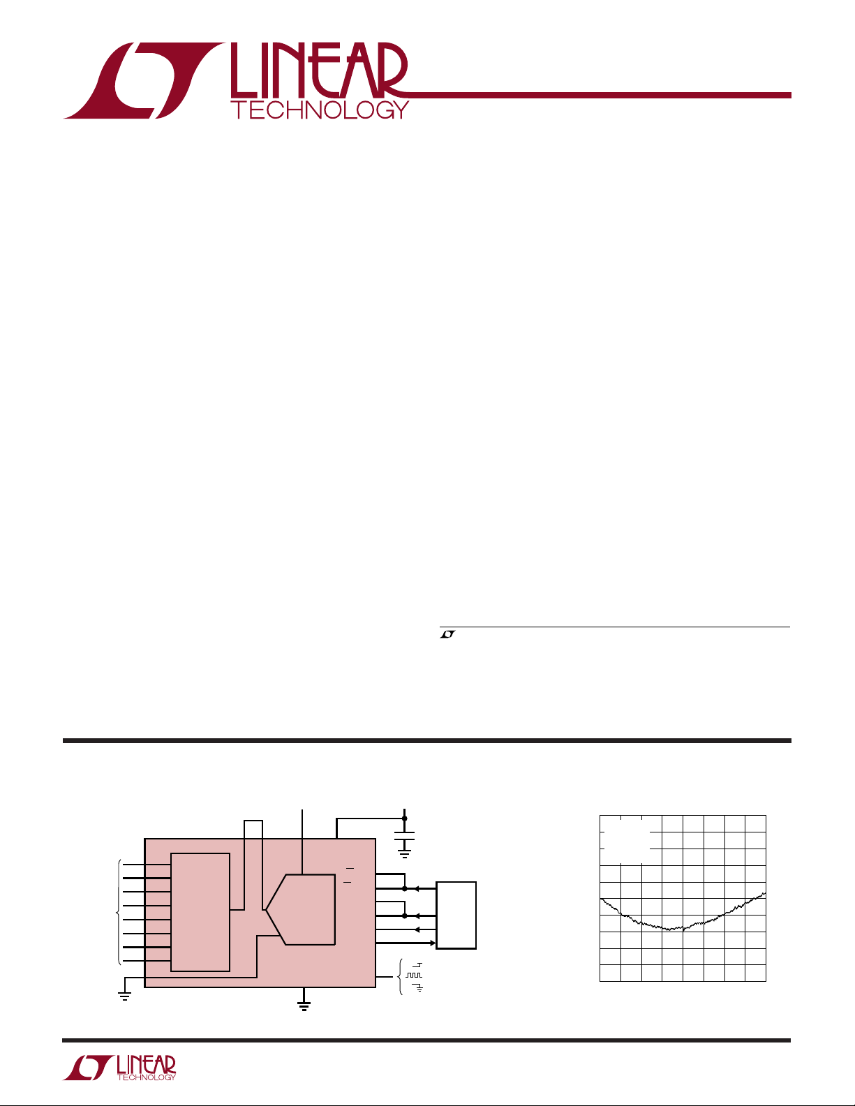
TYPICAL APPLICATIO
7 4 3 2, 8
9
CH0
10
CH1
11
CH2
12
CH3
CH4*
CH5*
CH6*
CH7*
6 COM
4-/8-CHANNEL
MUX
1, 5, 16, 18, 22, 27, 28
13
14
15
17
*THESE PINS ARE NO CONNECTS ON THE LTC2404
–0.12V
ANALOG
INPUTS
REF
1.12V
TO
REF
U
0.1V TO V
V
ADCINMUXOUT
24-BIT
+
∆∑ ADC
–
LTC2404/LTC2408
GND
CC
REFVCC
CSADC
CSMUX
SCK
CLK
D
SDO
2404/08 TA01
IN
F
O
2.7V TO 5.5V
23
20
19
25
21
24
26
1µF
SERIAL DATA LINK
MICROWIRE AND
SPI COMPATABLE
MPU
V
CC
= INTERNAL OSC/50Hz REJECTION
= EXTERNAL CLOCK SOURCE
= INTERNAL OSC/60Hz REJECTION
Total Unadjusted Error vs Output Code
10
VDD = 5V
8
= 5V
V
REF
= 25°C
T
A
6
= LOW
F
O
4
2
0
–2
–4
LINEARITY ERROR (ppm)
–6
–8
–10
0 8,338,608 16,777,215
OUTPUT CODE (DECIMAL)
2404/08 TA02
1
Page 2
LTC2404/LTC2408
WW
W
U
ABSOLUTE MAXIMUM RATINGS
(Notes 1, 2)
Supply Voltage (VCC) to GND.......................– 0.3V to 7V
Analog Input Voltage to GND ....... –0.3V to (VCC + 0.3V)
Reference Input Voltage to GND .. –0.3V to (VCC + 0.3V)
Digital Input Voltage to GND........ –0.3V to (VCC + 0.3V)
Digital Output Voltage to GND ..... –0.3V to (VCC + 0.3V)
U
W
PACKAGE/ORDER INFORMATION
ORDER
PART NUMBER
LTC2404CG
LTC2404IG
GND
V
V
REF
ADCIN
GND
COM
MUXOUT
V
CH0
CH1
CH2
CH3
NC
NC
TOP VIEW
1
2
CC
3
4
5
6
7
8
CC
9
10
11
12
13
14
28
27
26
25
24
23
22
21
20
19
18
17
16
15
GND
GND
F
O
SCK
SDO
CSADC
GND
D
IN
CSMUX
CLK
GND
NC
GND
NC
Operating Temperature Range
LTC2404C/LTC2408C ..............................0°C to 70°C
LTC2404I/LTC2408I ........................... – 40°C to 85°C
Storage Temperature Range ................. –65°C to 150°C
Lead Temperature (Soldering, 10 sec).................. 300°C
U
ORDER
PART NUMBER
LTC2408CG
LTC2408IG
GND
V
V
REF
ADCIN
GND
COM
MUXOUT
V
CH0
CH1
CH2
CH3
CH4
CH5
TOP VIEW
1
2
CC
3
4
5
6
7
8
CC
9
10
11
12
13
14
28
27
26
25
24
23
22
21
20
19
18
17
16
15
GND
GND
F
O
SCK
SDO
CSADC
GND
D
IN
CSMUX
CLK
GND
CH7
GND
CH6
G PACKAGE
28-LEAD PLASTIC SSOP
T
= 125°C, θJA = 130°C/W
JMAX
G PACKAGE
28-LEAD PLASTIC SSOP
T
= 125°C, θJA = 130°C/W
JMAX
Consult factory for Military grade parts.
U
CONVERTER CHARACTERISTICS
temperature range, otherwise specifications are at TA = 25°C. (Notes 3, 4)
PARAMETER CONDITIONS MIN TYP MAX UNITS
Resolution (No Missing Codes) 2.5V ≤ V
Integral Nonlinearity V
REF
V
REF
Offset Error 2.5V ≤ V
Offset Error Drift 2.5V ≤ V
Full-Scale Error 2.5V ≤ V
Full-Scale Error Drift 2.5V ≤ V
Total Unadjusted Error V
REF
V
REF
Output Noise VIN = 0V (Note 13) 1.5 µV
Normal Mode Rejection 60Hz ±2% (Note 7) ● 110 130 dB
≤ VCC, (Note 5) ● 24 Bits
REF
= 2.5V (Note 6) ● 2 10 ppm of V
= 5V (Note 6) ● 4 15 ppm of V
≤ V
REF
≤ V
REF
≤ V
REF
≤ V
REF
= 2.5V 5 ppm of V
= 5V 10 ppm of V
The ● denotes specifications which apply over the full operating
CC
CC
CC
CC
● 0.5 2 ppm of V
0.01 ppm of V
● 4 10 ppm of V
0.02 ppm of V
REF
REF
REF
REF
REF
/°C
REF
/°C
REF
REF
RMS
2
Page 3
LTC2404/LTC2408
U
CONVERTER CHARACTERISTICS
temperature range, otherwise specifications are at TA = 25°C. (Notes 3, 4)
PARAMETER CONDITIONS MIN TYP MAX UNITS
Normal Mode Rejection 50Hz ±2% (Note 8) ● 110 130 dB
Power Supply Rejection DC V
Power Supply Rejection 60Hz ±2% V
Power Supply Rejection 50Hz ±2% V
= 2.5V, VIN = 0V 100 dB
REF
= 2.5V, VIN = 0V, (Note 7) 110 dB
REF
= 2.5V, VIN = 0V, (Note 8) 110 dB
REF
The ● denotes specifications which apply over the full operating
UU
U
A ALOG I PUT A D REFERE CE
U
The ● denotes specifications which apply over the full operating
temperature range, otherwise specifications are at TA = 25°C. (Note 3)
SYMBOL PARAMETER CONDITIONS MIN TYP MAX UNITS
V
IN
V
REF
C
S(IN)
C
S(REF)
I
IN(LEAK)
I
REF(LEAK)
I
IN(MUX)
R
ON
I
S(OFF)
I
D(OFF)
t
OPEN
t
ON
t
OFF
QIRR MUX Off Isolation VIN = 2V
QINJ Charge Injection RS = 0Ω, CL = 1000pF, VS = 1V ±1pC
C
S(OFF)
C
D(OFF)
Input Voltage Range (Note 14) ● –0.125 • V
Reference Voltage Range ● 0.1 V
Input Sampling Capacitance 10 pF
Reference Sampling Capacitance 15 pF
Input Leakage Current CS = V
Reference Leakage Current V
On Channel Leakage Current VS = 2.5V (Note 15) ● ±20 nA
MUX On-Resistance I
MUX ∆RON vs Temperature 0.5 %/°C
∆RON vs VS (Note 15) 20 %
MUX Off Input Leakage Channel Off, VS = 2.5V ● ±20 nA
MUX Off Output Leakage Channel Off, VD = 2.5V ● ±20 nA
MUX Break-Before-Make Interval 125 290 ns
Enable Turn-On Time VS = 1.5V, RL = 3.4k, CL = 15pF 490 ns
Enable Turn-Off Time VS = 1.5V, RL = 3.4k, CL = 15pF 190 ns
Input Off Capacitance (MUX) 10 pF
Output Off Capacitance (MUX) 10 pF
CC
= 2.5V, CS = V
REF
= 1mA, VCC = 2.7V ● 250 300 Ω
OUT
= 1mA, VCC = 5V ● 120 250 Ω
I
OUT
P-P
CC
, RL = 1k, f = 100kHz 70 dB
● –10 1 10 nA
● –12 1 12 nA
REF
1.125 • V
CC
REF
V
V
3
Page 4

LTC2404/LTC2408
UU
DIGITAL I PUTS A D DIGITAL OUTPUTS
operating temperature range, otherwise specifications are at TA = 25°C. (Note 3)
SYMBOL PARAMETER CONDITIONS MIN TYP MAX UNITS
V
IH
V
IL
V
IH
V
IL
I
IN
I
IN
C
IN
C
IN
V
OH
V
OL
V
OH
V
OL
I
OZ
VIN H
VIN L
MUX
MUX
High Level Input Voltage 2.7V ≤ VCC ≤ 5.5V ● 2.5 V
CS, F
O
Low Level Input Voltage 4.5V ≤ VCC ≤ 5.5V ● 0.8 V
CS, F
O
High Level Input Voltage 2.7V ≤ VCC ≤ 5.5V (Note 9) ● 2.5 V
SCK 2.7V ≤ V
Low Level Input Voltage 4.5V ≤ VCC ≤ 5.5V (Note 9) ● 0.8 V
SCK 2.7V ≤ V
Digital Input Current 0V ≤ VIN ≤ V
CS, F
O
Digital Input Current 0V ≤ VIN ≤ VCC (Note 9) ● –10 10 µA
SCK
Digital Input Capacitance 10 pF
CS, F
O
Digital Input Capacitance (Note 9) 10 pF
SCK
High Level Output Voltage IO = –800µA ● VCC – 0.5V V
SDO
Low Level Output Voltage IO = 1.6mA ● 0.4V V
SDO
High Level Output Voltage IO = –800µA (Note 10) ● VCC – 0.5V V
SCK
Low Level Output Voltage IO = 1.6mA (Note 10) ● 0.4V V
SCK
High-Z Output Leakage ● –10 10 µA
SDO
MUX High Level Input Voltage V+ = 3V ● 2V
MUX Low Level Input Voltage V+ = 2.4V ● 0.8 V
2.7V ≤ VCC ≤ 3.3V 2.0 V
2.7V ≤ VCC ≤ 5.5V 0.6 V
≤ 3.3V (Note 9) 2.0 V
CC
≤ 5.5V (Note 9) 0.6 V
CC
CC
The ● denotes specifications which apply over the full
● –10 10 µA
WU
POWER REQUIRE E TS
otherwise specifications are at TA = 25°C. (Note 3)
SYMBOL PARAMETER CONDITIONS MIN TYP MAX UNITS
V
CC
I
CC
I
CC(MUX)
Supply Voltage ● 2.7 5.5 V
Supply Current
Conversion Mode CS = 0V (Note 12)
Sleep Mode CS = V
Multiplexer Supply Current All Logic Inputs Tied Together ● 15 40 µA
The ● denotes specifications which apply over the full operating temperature range,
● 200 300 µA
(Note 12) ● 20 30 µA
CC
= 0V or 5V
V
IN
4
Page 5
LTC2404/LTC2408
UW
TI I G CHARACTERISTICS
otherwise specifications are at TA = 25°C. (Note 3)
SYMBOL PARAMETER CONDITIONS MIN TYP MAX UNITS
f
EOSC
t
HEO
t
LEO
t
CONV
f
ISCK
D
ISCK
f
ESCK
t
LESCK
t
HESCK
t
DOUT_ISCK
t
DOUT_ESCK
t
1
t
2
t
3
t
4
t
KQMAX
t
KQMIN
t
5
t
6
External Oscillator Frequency Range ● 2.56 307.2 kHz
External Oscillator High Period ● 0.5 390 µs
External Oscillator Low Period ● 0.5 390 µs
Conversion Time FO = 0V ● 130.66 133.33 136 ms
Internal SCK Frequency Internal Oscillator (Note 10) 19.2 kHz
Internal SCK Duty Cycle (Note 10) 45 55 %
External SCK Frequency Range (Note 9) ● 2000 kHz
External SCK Low Period (Note 9) ● 250 ns
External SCK High Period (Note 9) ● 250 ns
Internal SCK 32-Bit Data Output Time Internal Oscillator (Notes 10, 12) ● 1.64 1.67 1.70 ms
External SCK 32-Bit Data Output Time (Note 9) ● 32/f
CS ↓ to SDO Low Z ● 0 150 ns
CS ↑ to SDO High Z ● 0 150 ns
CS ↓ to SCK ↓ (Note 10) ● 0 150 ns
CS ↓ to SCK ↑ (Note 9) ● 50 ns
SCK ↓ to SDO Valid ● 200 ns
SDO Hold After SCK ↓ (Note 5) ● 15 ns
SCK Set-Up Before CS ↓ ● 50 ns
SCK Hold After CS ↓ ● 50 ns
The ● denotes specifications which apply over the full operating temperature range,
= V
F
O
CC
External Oscillator (Note 11)
External Oscillator (Notes 10, 11) f
External Oscillator (Notes 10, 11)
● 156.80 160 163.20 ms
● 20480/f
● 256/f
(in kHz) ms
EOSC
/8 kHz
EOSC
(in kHz) ms
EOSC
(in kHz) ms
ESCK
Note 1: Absolute Maximum Ratings are those values beyond which the
life of the device may be impaired.
Note 2: All voltage values are with respect to GND.
Note 3: V
= 2.7 to 5.5V unless otherwise specified, source input
CC
is 0Ω.
Note 4: Internal Conversion Clock source with the F
to GND or to V
= 153600Hz unless otherwise specified.
f
EOSC
or to external conversion clock source with
CC
pin tied
O
Note 5: Guaranteed by design, not subject to test.
Note 6: Integral nonlinearity is defined as the deviation of a code from
a straight line passing through the actual endpoints of the transfer
curve. The deviation is measured from the center of the quantization
band.
Note 7: FO = 0V (internal oscillator) or f
= 153600Hz ±2%
EOSC
(external oscillator).
Note 8: F
= VCC (internal oscillator) or f
O
= 128000Hz ±2%
EOSC
(external oscillator).
Note 9: The converter is in external SCK mode of operation such that
the SCK pin is used as digital input. The frequency of the clock signal
driving SCK during the data output is f
and is expressed in kHz.
ESCK
Note 10: The converter is in internal SCK mode of operation such that
the SCK pin is used as digital output. In this mode of operation the
SCK pin has a total equivalent load capacitance C
Note 11: The external oscillator is connected to the F
oscillator frequency, f
, is expressed in kHz.
EOSC
= 20pF.
LOAD
pin. The external
O
Note 12: The converter uses the internal oscillator.
F
= 0V or FO = VCC.
O
Note 13: The output noise includes the contribution of the internal
calibration operations.
Note 14: For reference voltage values V
of –0.125 • V
to 1.125 • V
REF
is limited by the absolute maximum
REF
rating of the Analog Input Voltage pin (Pin 3). For 2.5V < V
0.267V + 0.89 • V
For 0.267V + 0.89 • V
+ 0.3V.
to V
CC
the input voltage range is –0.3V to 1.125 • V
CC
< V
CC
≤ VCC the input voltage range is –0.3V
REF
> 2.5V the extended input
REF
REF
≤
REF
Note 15: VS is the voltage applied to a channel input. VD is the voltage
applied to the MUX output.
.
5
Page 6
LTC2404/LTC2408
UW
TYPICAL PERFOR A CE CHARACTERISTICS
Total Unadjusted Error
(3V Supply) INL (3V Supply)
10
VCC = 3V
= 3V
V
REF
5
0
ERROR (ppm)
–5
–10
0
TA = –55°C, –45°C, 25°C, 90°C
0.5 1.0 1.5 2.0
INPUT VOLTAGE (V)
Positive Extended Input Range
Total Unadjusted Error (3V Supply)
10
= 3V
V
CC
= 3V
V
REF
5
= –55°C
T
A
0
ERROR (ppm)
–5
–10
3.0
TA = 90°C TA = 25°C
3.1 3.2
INPUT VOLTAGE (V)
TA = –45°C
2.5 3.0
24048 G01
3.3
24048 G04
10
VCC = 3V
V
REF
5
0
ERROR (ppm)
–5
–10
0
Total Unadjusted Error
(5V Supply)
10
VCC = 5V
8
= 5V
V
REF
6
4
2
0
–2
ERROR (ppm)
–4
–6
–8
–10
0
= 3V
TA = –55°C, –45°C, 25°C, 90°C
0.5 1.0 1.5 2.0
INPUT VOLTAGE (V)
TA = –55°C, –45°C, 25°C, 90°C
1
INPUT VOLTAGE (V)
3
2
2.5 3.0
24048 G02
4
24048 G05
5
Negative Extended Input Range
Total Unadjusted Error (3V Supply)
10
VCC = 3V
= 3V
V
REF
5
0
ERROR (ppm)
–5
–10
–0.050
TA = 90°C
TA = 25°C
TA = –45°C
TA = –55°C
INPUT VOLTAGE (V)
INL (5V Supply)
10
VCC = 5V
= 5V
V
REF
5
0
ERROR (ppm)
–5
–10
TA = –55°C, –45°C, 25°C, 90°C
1
0
2
INPUT VOLTAGE (V)
3
–0.30
–0.25–0.20–0.15–0.10
24048 G03
4
5
24048 G06
Negative Extended Input Range
Total Unadjusted Error (5V Supply) Offset Error vs Reference Voltage
10
VCC = 5V
= 5V
V
REF
5
0
ERROR (ppm)
–5
–10
–0.050
INPUT VOLTAGE (V)
TA = 90°C
TA = 25°C
TA = –45°C
TA = –55°C
–0.30
–0.25–0.20–0.15–0.10
24048 G07
Positive Extended Input Range
Total Unadjusted Error (5V Supply)
10
V
= 5V
CC
= 5V
V
REF
5
0
ERROR (ppm)
–5
–10
5.0
TA = 90°C TA = 25°C
5.1 5.2
INPUT VOLTAGE (V)
T
TA = –45°C
= –55°C
A
24048 G08
5.3
20
)
15
REF
10
5
RMS NOISE (ppm OF V
0
1
0
REFERENCE VOLTAGE (V)
3
2
6
VCC = 5V
T
= 25°C
A
4
24048 G10
5
Page 7
UW
V
CC
2.7
RMS NOISE (ppm)
0
2.5
5.0
3.2 3.7 4.2 4.7
24048 G12
5.2
V
REF
= 2.5V
T
A
= 25°C
TEMPERATURE (°C)
–50
–5.0
OFFSET ERROR (ppm)
–2.5
0
2.5
5.0
–25 0 25 50
24048 G15
75 100 125
VCC = 5V
V
REF
= 5V
V
IN
= 0V
V
CC
2.7
0
FULL-SCALE ERROR (ppm)
2
1
3
5
4
6
3.2 3.7 4.2 4.7
24048 G18
5.2
V
REF
= 2.5V
V
IN
= 2.5V
T
A
= 25°C
TYPICAL PERFOR A CE CHARACTERISTICS
LTC2404/LTC2408
RMS Noise vs Reference Voltage Offset Error vs V
20
)
15
REF
10
5
RMS NOISE (ppm OF V
0
1
0
REFERENCE VOLTAGE (V)
VCC = 5V
T
= 25°C
A
3
4
2
5
24048 G10
5.0
V
REF
T
= 25°C
A
2.5
0
OFFSET ERROR (ppm)
–2.5
–5.0
2.7
RMS Noise vs CODE OUT
1500
1000
V
= 5V
CC
= 5V
V
REF
= 0V
V
IN
1.00
0.75
0.50
VCC = 5V
V
REF
= –0.3V TO 5.3V
V
IN
= 25°C
T
A
CC
= 2.5V
3.2 3.7 4.2 4.7
= 5V
V
CC
5.2
24048 G11
RMS Noise vs V
Offset Error vs TemperatureNoise Histogram
CC
500
NUMBER OF READINGS
0
5.0
2.5
0
–2.5
FULL-SCALE ERROR (ppm)
–5.0
–0.5 0 0.5 1.0
OUTPUT CODE (ppm)
Full-Scale Error vs Temperature
VCC = 5V
V
REF
= 5V
V
IN
–50
–25 0 25 50
TEMPERATURE (°C)
75 100 125
24048 G13
= 5V
24048 G16
RMS NOISE (ppm)
0.25
1.5–1.0
0
0
7FFFFF
CODE OUT (HEX)
FFFFFF
24048 G14
Full-Scale Error
vs Reference Voltage
10.0
7.5
5.0
2.5
FULL-SCALE ERROR (ppm)
0
1
0
REFERENCE VOLTAGE (V)
VCC = 5V
= V
V
IN
REF
3
4
2
5
24048 G17
Full-Scale Error vs V
CC
7
Page 8
LTC2404/LTC2408
INPUT FREQUENCY
0
–60
–40
0
24048 F23
–80
–100
fS/2 f
S
–120
–140
–20
REJECTION (dB)
UW
TYPICAL PERFOR A CE CHARACTERISTICS
Conversion Current vs Temperature
230
220
210
200
190
180
SUPPLY CURRENT (µA)
170
160
150
–50
PSRR vs Frequency at V
–10
VCC = 4.1V
V
IN
–30
= 25°C
T
A
= 0
F
0
–50
–70
VCC = 5.5V
VCC = 4.1V
VCC= 2.7V
–25 0 50
= 0V
25
TEMPERATURE (°C)
75 100 125
CC
24048 G19
Sleep Current vs Temperature
30
25
20
15
10
SUPPLY CURRENT (µA)
5
0
–50
–25 0
VCC = 5.5V
V
CC
50 100 125
25 75
TEMPERATURE (°C)
PSRR vs Frequency at V
0
VCC = 4.1V
= 0V
V
IN
–20
= 25°C
T
A
= 0
F
O
–40
–60
= 2.7V
CC
24048 G20
PSRR vs Frequency at V
0
VCC = 4.1V
= 0V
V
IN
–20
= 25°C
T
A
= 0
F
O
–40
–60
REJECTION (dB)
–80
–100
–120
1
15,360Hz 153,600Hz
100 10k 1M
FREQUENCY AT VCC (Hz)
Rejection vs Frequency at V
0
–20
–40
–60
CC
VCC = 5V
V
REF
V
IN
F
O
24048 G21
IN
= 5V
= 2.5V
= 0
REJECTION (dB)
REJECTION (dB)
–90
–110
–130
0
50 100 150 200
FREQUENCY AT V
(Hz)
CC
Rejection vs Frequency at V
–60
–70
–80
–90
–100
–110
–120
–130
–140
–12–8–404812
INPUT FREQUENCY DEVIATION FROM NOTCH FREQUENCY (%)
250
24048 G22
IN
24048 G25
REJECTION (dB)
–80
–100
–120
15200
15300 15350 15400
15250
FREQUENCY AT VCC (Hz)
Rejection vs Frequency at V
0
VCC = 5V
= 5V
V
REF
–20
= 2.5V
V
IN
= 0
F
O
–40
–60
REJECTION (dB)
–80
–100
–120
SAMPLE RATE = 15.36kHz ±2%
15100
15200 15300 15400 15500
FREQUENCY AT VIN (Hz)
15450 15500
24048 G23
IN
24048 G26
REJECTION (dB)
–80
–100
–120
1
50 100 150 200
FREQUENCY AT VIN (Hz)
Rejection vs Frequency at V
250
24048 G24
IN
8
Page 9
UW
TYPICAL PERFOR A CE CHARACTERISTICS
INL vs Maximum Output Rate
24
22
20
18
16
INL (BITS)
14
12
10
8
0
VCC = 5V
V
= 5V
REF
F
= EXTERNAL
0
(20480 × MAXIMUM
OUTPUT RATE)
TA = 25°C
T
= 90°C
A
15 20 25105 303540455055
MAXIMUM OUTPUT RATE (Hz)
60
24048 G27
24
22
20
18
16
14
RESOLUTION (BITS)*
12
10
8
LTC2404/LTC2408
Resolution vs Maximum
Output Rate
FO = EXTERNAL
(20480 × MAXIMUM
OUTPUT RATE)
T
T
VCC = V
VCC = V
= 3V
REF
/RMS NOISE)
LOG(V
*RESOLUTION =
0
15 20 25105 303540455055
MAXIMUM OUTPUT RATE (Hz)
REF
LOG (2)
= 25°C
A
= 90°C
A
REF
= 5V
60
24048 G28
U
UU
PIN FUNCTIONS
GND (Pins 1, 5, 16, 18, 22, 27, 28): Ground. Should be
connected directly to a ground plane through a minimum
length trace or it should be the single-point-ground in a
single point grounding system.
VCC (Pins 2, 8): Positive Supply Voltage. 2.7V ≤ VCC ≤
5.5V. Bypass to GND with a 10µF tantalum capacitor in
parallel with 0.1µF ceramic capacitor as close to the part
as possible.
V
(Pin 3): Reference Input. The reference voltage range
REF
is 0.1V to VCC.
ADCIN (Pin 4): Analog Input. The input voltage range is
–0.125 • V
voltage range may be limited by the pin absolute maximum rating of –0.3V to VCC + 0.3V.
COM (Pin 6): Signal Ground. Should be connected directly
to a ground plane through minimum length trace.
MUXOUT (Pin 7): MUX Output. This pin is the output of the
multiplexer. Tie to ADCIN for normal operation.
CH0 (Pin 9): Analog Multiplexer Input.
to 1.125 • V
REF
REF
. For V
> 2.5V the input
REF
CH4 (Pin 13): Analog Multiplexer Input. No connect on the
LTC2404.
CH5 (Pin 14): Analog Multiplexer Input. No connect on the
LTC2404.
CH6 (Pin 15): Analog Multiplexer Input. No connect on the
LTC2404.
CH7 (Pin 17): Analog Multiplexer Input. No connect on the
LTC2404.
CLK (Pin 19): Shift Clock for Data In. This clock synchronizes the serial data transfer into the MUX. For normal
operation, drive this pin in parallel with SCK.
CSMUX (Pin 20): MUX Chip Select Input. A logic high on
this input allows the MUX to receive a channel address. A
logic low enables the selected MUX channel and connects
it to the MUXOUT pin for A/D conversion. For normal
operation, drive this pin in parallel with CSADC.
DIN (Pin 21): Digital Data Input. The multiplexer address
is shifted into this input on the last four rising CLK edges
before CSMUX goes low.
CH1 (Pin 10): Analog Multiplexer Input.
CH2 (Pin 11): Analog Multiplexer Input.
CH3 (Pin 12): Analog Multiplexer Input.
CSADC (Pin 23): ADC Chip Select Input. A low on this pin
enables the SDO digital output and following each conversion, the ADC automatically enters the Sleep mode and
remains in this low power state as long as CSADC is high.
9
Page 10
LTC2404/LTC2408
3.4k
SDO
24048 TC02
HI-Z TO V
OL
VOH TO V
OL
VOL TO HI-Z
C
LOAD
= 20pF
V
CC
U
UU
PIN FUNCTIONS
A high on this pin also disables the SDO digital output. A
low-to-high transition on CSADC during the Data Output
state aborts the data transfer and starts a new conversion.
For normal operation, drive this pin in parallel with CSMUX.
SDO (Pin 24): Three-State Digital Output. During the data
output period this pin is used for serial data output. When
the chip select CSADC is high (CSADC = VCC), the SDO pin
is in a high impedance state. During the Conversion and
Sleep periods, this pin can be used as a conversion status
output. The conversion status can be observed by pulling
CSADC low.
SCK (Pin 25): Shift Clock for Data Out. This clock synchronizes the serial data transfer of the ADC data output. Data
UU
W
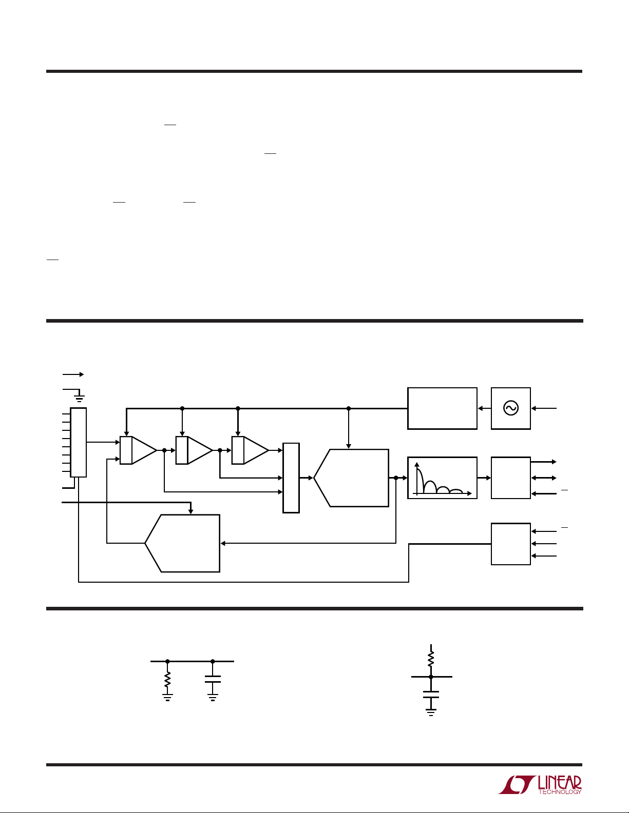
FU CTIO AL BLOCK DIAGRA
V
CC
GND
CH0
CH1
CH2
CH3
CH4
CH5
CH6
CH7
COM
V
REF
8-CHANNEL MUX
∫∫∫
∑
is shifted out of SDO on the falling edge of SCK. For normal
operation, drive this pin in parallel with CLK.
FO (Pin 26): Digital input which controls the ADC’s notch
frequencies and conversion time. When the FO pin is
connected to VCC (FO = VCC), the converter uses its internal
oscillator and the digital filter first null is located at 50Hz.
When the FO pin is connected to GND (FO = OV), the
converter uses its internal oscillator and the digital filter
first null is located at 60Hz. When FO is driven by an
external clock signal with a frequency f
, the converter
EOSC
uses this signal as its clock and the digital filter first null is
located at a frequency f
word rate is f
ADC
EOSC
/20480.
AUTOCALIBRATION
AND CONTROL
DECIMATING FIR
/2560. The resulting output
EOSC
INTERNAL
OSCILLATOR
(INT/EXT)
SERIAL
INTERFACE
F
O
SDO
SCK
CSADC
TEST CIRCUITS
10
SDO
DAC
3.4k
HI-Z TO V
VOL TO V
OH
VOH TO HI-Z
24048 BD
CSMUX
D
IN
CLK
CHANNEL
SELECT
= 20pF
C
LOAD
OH
24048 TC01
Page 11
LTC2404/LTC2408
U
WUU
APPLICATIONS INFORMATION
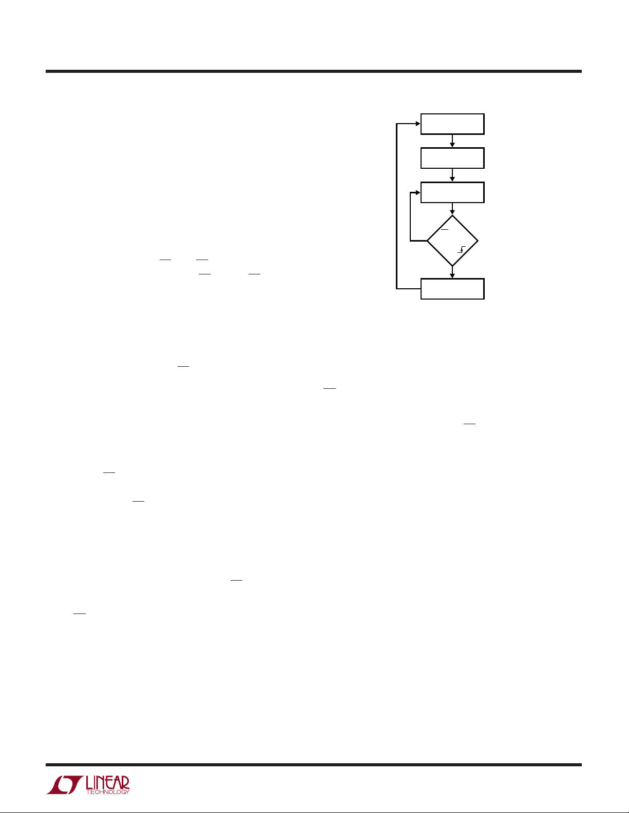
Converter Operation Cycle
The LTC2404/LTC2408 are low power, 4-/8-channel deltasigma analog-to-digital converters with easy-to-use
4-wire interfaces. Their operation is simple and made up
of four states. The converter operation begins with the
conversion, followed by a low power sleep state and
concluded with the data output (see Figure 1). Channel
selection may be performed while the device is in the sleep
state or at the conclusion of the data output state. The
interface consists of serial data output (SDO), serial clock
(CLK/SCK), chip select (CSADC/CSMUX) and data input
(DIN). By tying SCK to CLK and CSADC to CSMUX, the
interface requires only four wires.
Initially, the LTC2404 or LTC2408 performs a conversion.
Once the conversion is complete, the device enters the
sleep state. While in the sleep state, power consumption
is reduced by an order of magnitude. The part remains in
the sleep state as long as CSADC is logic HIGH. The
conversion result is held indefinitely in a static shift
register while the converter is in the sleep state.
Channel selection for the next conversion cycle is performed while the device is in the sleep state or at the end
of the data output state. A specific channel is selected by
applying a 4-bit serial word to the DIN pin on the rising edge
of CLK while CSMUX is HIGH, see Figure 3 and Table 3. The
channel is selected based on the last four bits clocked into
the DIN pin before CSMUX goes low. If DIN is all 0’s, the
previous channel remains selected.
CONVERT
CHANNEL SELECT
(SLEEP)
SLEEP
CSADC
1
AND
SCK
0
DATA OUTPUT
(CHANNEL SELECT)
Figure 1. LTC2408 State Transition Diagram
24048 F01
edge of SCK, see Figure 3. The data output state is
concluded once 32 bits are read out of the ADC or when
CSADC is brought HIGH. The device automatically initiates
a new conversion and the cycle repeats.
Through timing control of the CSADC and SCK pins, the
LTC2404/LTC2408 offer two modes of operation: internal
or external SCK. These modes do not require programming configuration registers; moreover, they do not disturb the cyclic operation described above. These modes of
operation are described in detail in the Serial Interface
Timing Modes section.
In the example, Figure 3, the MUX channel is selected
during the sleep state, just before the data output state
begins. Once the channel selection is complete, the device
remains in the sleep state as long as CSADC remains
HIGH.
Once CSADC is pulled low, the device begins outputting
the conversion result. There is no latency in the conversion
result. Since there is no latency, the first conversion
following a change in input channel is valid and corresponds to that channel. The data output corresponds to
the conversion just performed. This result is shifted out on
the serial data output pin (SDO) under the control of the
serial clock (SCK). Data is updated on the falling edge of
SCK allowing the user to reliably latch data on the rising
Conversion Clock
A major advantage delta-sigma converters offer over
conventional type converters is an on-chip digital filter
(commonly known as Sinc or Comb filter). For high
resolution, low frequency applications, this filter is typically designed to reject line frequencies of 50 or 60Hz plus
their harmonics. In order to reject these frequencies in
excess of 110dB, a highly accurate conversion clock is
required. The LTC2404/LTC2408 incorporate an on-chip
highly accurate oscillator. This eliminates the need for
external frequency setting components such as crystals or
oscillators. Clocked by the on-chip oscillator, the LTC2404/
LTC2408 reject line frequencies (50 or 60Hz ±2%) a
minimum of 110dB.
11
Page 12

LTC2404/LTC2408
U
WUU
APPLICATIONS INFORMATION
Ease of Use
The LTC2404/LTC2408 data output has no latency, filter
settling or redundant data associated with the conversion
cycle. There is a one-to-one correspondence between the
conversion and the output data. Therefore, multiplexing
an analog input voltage is easy.
The LTC2404/LTC2408 perform offset and full-scale calibrations every conversion cycle. This calibration is transparent to the user and has no effect on the cyclic operation
described above. The advantage of continuous calibration
is extreme stability of offset and full-scale readings with
respect to time, supply voltage change and temperature
drift.
Power-Up Sequence
The LTC2404/LTC2408 automatically enter an internal
reset state when the power supply voltage VCC drops
below approximately 2.2V. When the VCC voltage rises
above this critical threshold, the converter creates an
internal power-on-reset (POR) signal with duration of
approximately 0.5ms. The POR signal clears all internal
registers within the ADC and initiates a conversion. At
power-up, the multiplexer channel is disabled and should
be programmed once the device enters the sleep state.
The results of the first conversion following a POR are not
valid since a multiplexer channel was disabled.
Reference Voltage Range
The LTC2404/LTC2408 can accept a reference voltage
from 0V to VCC. The converter output noise is determined
by the thermal noise of the front-end circuits, and as such,
its value in microvolts is nearly constant with reference
voltage. A decrease in reference voltage will not significantly improve the converter’s effective resolution. On the
other hand, a reduced reference voltage will improve the
overall converter INL performance. The recommended
range for the LTC2404/LTC2408 voltage reference is
100mV to VCC.
Input Voltage Range
The converter is able to accommodate system level offset
and gain errors as well as system level overrange
situations due to its extended input range, see Figure 2.
VCC + 0.3V
9/8V
REF
V
REF
NORMAL
1/2V
REF
0
–1/8V
REF
–0.3V
Figure 2. LTC2404/LTC2408 Input Range
INPUT
RANGE
EXTENDED
INPUT
RANGE
ABSOLUTE
MAXIMUM
INPUT
RANGE
24048 F02
The LTC2404/LTC2408 converts input signals within the
extended input range of –0.125 • V
For large values of V
this range is limited to a voltage
REF
to 1.125 • V
REF
REF
.
range of – 0.3V to (VCC + 0.3V). Beyond this range the input
ESD protection devices begin to turn on and the errors due
to the input leakage current increase rapidly.
Input signals applied to VIN may extend below ground by
– 300mV and above VCC by 300mV. In order to limit any fault
current, a resistor of up to 5k may be added in series with
any channel input pin (CH0 to CH7) without affecting the
performance of the device. In the physical layout, it is important to maintain the parasitic capacitance of the connection between this series resistance and the channel input
pin as low as possible; therefore, the resistor should be
located as close as practical to the channel input pin. The
effect of the series resistance on the converter accuracy can
be evaluated from the curves presented in the Analog Input/Reference Current section. In addition, a series resistor will introduce a temperature dependent offset error due
to the input leakage current. A 1nA input leakage current
will develop a 1ppm offset error on a 5k resistor if V
REF
=
5V. This error has a very strong temperature dependency.
Output Data Format
The LTC2404/LTC2408 serial output data stream is 32 bits
long. The first 4 bits represent status information indicating the sign, input range and conversion state. The next 24
bits are the conversion result, MSB first. The remaining 4
bits are sub LSBs beyond the 24-bit level that may be included in averaging or discarded without loss of resolution.
12
Page 13

LTC2404/LTC2408
U
WUU
APPLICATIONS INFORMATION
Bit 31 (first output bit) is the end of conversion (EOC)
indicator. This bit is available at the SDO pin during the
conversion and sleep states whenever the CSADC pin is
LOW. This bit is HIGH during the conversion and goes
LOW when the conversion is complete.
Bit 30 (second output bit) is a dummy bit (DMY) and is
always LOW.
Bit 29 (third output bit) is the conversion result sign indicator (SIG). If VIN is >0, this bit is HIGH. If VIN is <0, this
bit is LOW. The sign bit changes state during the zero code.
Bit 28 (forth output bit) is the extended input range (EXR)
indicator. If the input is within the normal input range
0␣ ≤␣VIN ≤ V
normal input range, VIN > V
, this bit is LOW. If the input is outside the
REF
or VIN < 0, this bit is HIGH.
REF
The function of these bits is summarized in Table 1.
Table 1. LTC2404/LTC2408 Status Bits
Bit 31 Bit 30 Bit 29 Bit 28
Input Range EOC DMY SIG EXR
VIN > V
REF
0 < VIN ≤ V
VIN = 0+/0
VIN < 0 0 001
REF
–
0 011
0 010
0 0 1/0 0
Bit 27 (fifth output bit) is the most significant bit (MSB).
Bits 27-4 are the 24-bit conversion result MSB first.
Bit 4 is the least significant bit (LSB).
Bits 3-0 are sub LSBs below the 24-bit level. Bits 3-0 may
be included in averaging or discarded without loss of
resolution.
Data is shifted out of the SDO pin under control of the serial
clock (SCK), see Figure 3. Whenever CSADC is HIGH, SDO
remains high impedance and any SCK clock pulses are
ignored by the internal data out shift register.
In order to shift the conversion result out of the device,
CSADC must first be driven LOW. EOC is seen at the SDO
pin of the device once CSADC is pulled LOW. EOC changes
in real time from HIGH to LOW at the completion of a
conversion. This signal may be used as an interrupt for an
external microcontroller. Bit 31 (EOC) can be captured on
the first rising edge of SCK. Bit 30 is shifted out of the
device on the first falling edge of SCK. The final data bit
(Bit 0) is shifted out on the falling edge of the 31st SCK and
may be latched on the rising edge of the 32nd SCK pulse.
On the falling edge of the 32nd SCK pulse, SDO goes HIGH
indicating a new conversion cycle has been initiated. This
bit serves as EOC (Bit 31) for the next conversion cycle.
Table 2 summarizes the output data format.
As long as the voltage on the VIN pin is maintained within
the –0.3V to (VCC + 0.3V) absolute maximum operating
range, a conversion result is generated for any input value
from –0.125 • V
greater than 1.125 • V
to the value corresponding to 1.125 • V
voltages below –0.125 • V
clamped to the value corresponding to –0.125 • V
to 1.125 • V
REF
, the conversion result is clamped
REF
For input voltages
REF.
. For input
REF
, the conversion result is
REF
REF
.
CSMUX/CSADC
SDO
SCK/CLK
D
t
CONV
HI-Z
IN
D2EN D1 D0
EOC “0”
BIT 30BIT 31 BIT 0
Figure 3. Typical Data Input/Output Timing
MSB LSB
EXTSIG
DON’T CARE
HI-Z
24048 F03
13
Page 14

LTC2404/LTC2408
U
WUU
APPLICATIONS INFORMATION
Channel Selection
Typically, CSADC and CSMUX are tied together or CSADC
is inverted and drives CSMUX. SCK and CLK are tied
together and driven with a common clock signal. During
channel selection, CSMUX is HIGH. Data is shifted into the
DIN pin on the rising edge of CLK, see Figure 3. Table 3
shows the bit combinations for channel selection. In order
to enable the multiplexer output, CSMUX must be pulled
LOW. The multiplexer should be programmed after the
previous conversion is complete. In order to guarantee the
conversion is complete, the multiplexer addressing should
be delayed a minimum t
60Hz notch) after the data out is read.
While the multiplexer is being programmed, the ADC is in
a low power sleep state. Once the MUX addressing is
complete, the data from the preceding conversion can be
read. A new conversion cycle is initiated following the data
read cycle with the analog input tied to the newly selected
channel.
(approximately 133ms for a
CONV
Table 3. Logic Table for Channel Selection
CHANNEL STATUS EN D2 D1 D0
All Off 0 X X X
CH0 1000
CH1 1001
CH2 1010
CH3 1011
CH4* 1100
CH5* 1101
CH6* 1110
CH7* 1111
*Not used for the LTC2404.
Frequency Rejection Selection (FO Pin Connection)
The LTC2404/LTC2408 internal oscillator provides better
than 110dB normal mode rejection at the line frequency
and all its harmonics for 50Hz ±2% or 60Hz ±2%. For
60Hz rejection, FO (Pin 26) should be connected to GND
(Pin 1) while for 50Hz rejection the FO pin should be
connected to V
(Pin␣ 2).
CC
Table 2. LTC2404/LTC2408 Output Data Format
Bit 31 Bit 30 Bit 29 Bit 28 Bit 27 Bit 26 Bit 25 Bit 24 Bit 23 … Bit 4 Bit 3-0
Input Voltage EOC DMY SIG EXR MSB LSB SUB LSBs*
VIN > 9/8 • V
9/8 • V
V
REF
V
REF
3/4V
3/4V
1/2V
1/2V
1/4V
1/4V
0+/0
–1LSB 0 0 0111 1 11...1 X
–1/8 • V
VIN < –1/8 • V
*The sub LSBs are valid conversion results beyond the 24-bit level that may be included in averaging or discarded without loss of resolution.
**The sign bit changes state during the 0 code.
REF
REF
+ 1LSB 0 0 1 1 0 0 0 0 0 ... 0 X
+ 1LSB 0 0 1 0 1 1 0 0 0 ... 0 X
REF
REF
+ 1LSB 0 0 1 0 1 0 0 0 0 ... 0 X
REF
REF
+ 1LSB 0 0 1 0 0 1 0 0 0 ... 0 X
REF
REF
–
REF
REF
001100011...1X
001100011...1X
001011111...1X
001010111...1X
001001111...1X
001000111...1X
0 0 1/0** 0 0 0 0 0 0 ... 0 X
000111100...0X
000111100...0X
14
Page 15

LTC2404/LTC2408
U
WUU
APPLICATIONS INFORMATION
The selection of 50Hz or 60Hz rejection can also be made
by driving FO to an appropriate logic level. A selection
change during the sleep or data output states will not
disturb the converter operation. If the selection is made
during the conversion state, the result of the conversion in
progress may be outside specifications but the following
conversions will not be affected.
When a fundamental rejection frequency different from
50Hz or 60Hz is required or when the converter must be
synchronized with an outside source, the LTC2404/
LTC2408 can operate with an external conversion clock.
The converter automatically detects the presence of an
external clock signal at the FO pin and turns off the internal
oscillator. The frequency f
be at least 2560Hz (1Hz notch frequency) to be detected.
The external clock signal duty cycle is not significant as
long as the minimum and maximum specifications for the
high and low periods t
HEO
While operating with an external conversion clock of a
frequency f
, the LTC2404/LTC2408 provide better
EOSC
than 110dB normal mode rejection in a frequency range
f
/2560 ±4% and its harmonics. The normal mode
EOSC
rejection as a function of the input frequency deviation
from f
/2560 is shown in Figure 4.
EOSC
Whenever an external clock is not present at the FO pin the
converter automatically activates its internal oscillator
and enters the Internal Conversion Clock mode. The
of the external signal must
EOSC
and t
are observed.
LEO
–60
–70
–80
–90
–100
–110
REJECTION (dB)
–120
–130
–140
–12–8–404812
INPUT FREQUENCY DEVIATION FROM NOTCH FREQUENCY (%)
24048 F04
Figure 4. LTC2404/LTC2408 Normal Mode Rejection When
Using an External Oscillator of Frequency f
EOSC
LTC2404/LTC2408 operation will not be disturbed if the
change of conversion clock source occurs during the
sleep state or during the data output state while the
converter uses an external serial clock. If the change
occurs during the conversion state, the result of the
conversion in progress may be outside specifications but
the following conversions will not be affected. If the
change occurs during the data output state and the
converter is in the Internal SCK mode, the serial clock duty
cycle may be affected but the serial data stream will
remain valid.
Table 4 summarizes the duration of each state as a
function of FO.
Table 4. LTC2404/LTC2408 State Duration
State Operating Mode Duration
CONVERT Internal Oscillator FO = LOW (60Hz Rejection) 133ms
FO = HIGH (50Hz Rejection) 160ms
External Oscillator FO = External Oscillator 20480/f
with Frequency f
/2560 Rejection)
(f
EOSC
SLEEP As Long As CS = HIGH Until CS = 0 and SCK
DATA OUTPUT Internal Serial Clock FO = LOW/HIGH As Long As CS = LOW But Not Longer Than 1.67ms
(Internal Oscillator) (32 SCK cycles)
FO = External Oscillator with As Long As CS = LOW But Not Longer Than 256/f
MAXIMUM OUTPUT
WORD RATE
Frequency f
External Serial Clock with As Long As CS = LOW But Not Longer Than 32/f
Frequency f
kHz (32 SCK cycles)
SCK
EOSC
kHz
EOSC
kHz (32 SCK cycles)
OWR
(In Seconds)
EOSC
=
tt
CONVERT DATAOUTPUT
1
+
inHz
SCK
EOSC
ms
ms
15
Page 16

LTC2404/LTC2408
U
WUU
APPLICATIONS INFORMATION
Using an External Clock for Faster Conversion Times
The conversion time of the LTC2404/LTC2408 is determined by the conditions on the FO pin. If FO is connected
to GND for 60Hz rejection, the conversion time is 133µs.
If FO is connected to VCC, the conversion time is 160µs. For
an externally supplied frequency of f
version time is:
t
CONV
= 20480/f
EOSC
(kHz)
The resulting frequency rejection is:
Notch Frequency = 8/t
CONV
The maximum output word rate is:
OWR
=
tt
CONVERT DATAOUTPUT
24
22
20
18
16
INL (BITS)
14
12
10
8
0
Figure 5. INL vs Maximum Output Rate
24
22
20
18
16
VCC = V
14
RESOLUTION (BITS)*
12
10
*RESOLUTION =
8
0
Figure 6. Resolution vs Maximum Output Rate
1
+
VCC = 5V
= 5V
V
REF
= EXTERNAL
F
0
(20480 × MAXIMUM
OUTPUT RATE)
TA = 25°C
T
= 90°C
A
15 20 25105 303540455055
MAXIMUM OUTPUT RATE (Hz)
FO = EXTERNAL
(20480 × MAXIMUM
OUTPUT RATE)
T
= 25°C
A
= 90°C
T
A
VCC = V
= 3V
REF
/RMS NOISE)
LOG(V
REF
LOG (2)
15 20 25105 303540455055
MAXIMUM OUTPUT RATE (Hz)
(kHz), the con-
EOSC
inHz
60
24048 G27
= 5V
REF
60
24048 G28
The DC specifications are guaranteed for f
EOSC
up to a
maximum of 307.2kHz, resulting in a maximum output
word rate of approximately 15Hz. However, for faster rates
at reduced performance, frequencies up to 1.22MHz can
be used on the FO pin. Figures 5 and 6 show the INL and
Resolution vs Output Rate.
SERIAL INTERFACE
The LTC2404/LTC2408 transmit the conversion results,
program the channel selection, and receive the start of
conversion command through a synchronous 4-wire interface (SCK = CLK, CSADC = CSMUX). During the conversion and sleep states, this interface can be used to assess
the converter status. While in the sleep state this interface
may be used to program an input channel. During the data
output state it is used to read the conversion result.
ADC Serial Clock Input/Output (SCK)
The serial clock signal present on SCK (Pin 25) is used to
synchronize the data transfer. Each bit of data is shifted out
the SDO pin on the falling edge of the serial clock.
In the Internal SCK mode of operation, the SCK pin is an
output and the LTC2404/LTC2408 creates its own serial
clock by dividing the internal conversion clock by 8. In the
External SCK mode of operation, the SCK pin is used as
input. The internal or external SCK mode is selected on
power-up and then reselected every time a HIGH-to-LOW
transition is detected at the CSADC pin. If SCK is HIGH or
floating at power-up or during this transition, the converter
enters the internal SCK mode. If SCK is LOW at power-up
or during this transition, the converter enters the external
SCK mode.
Multiplexer Serial Input Clock (CLK)
Generally, this pin is externally tied to SCK for 4-wire operation. On the rising edge of CLK (Pin 19) with CSMUX held
HIGH, data is serially shifted into the multiplexer. If CSMUX
is LOW the CLK input will be disabled and the channel
selection unchanged.
Serial Data Output (SDO)
The serial data output pin, SDO (Pin 24), drives the serial
data during the data output state. In addition, the SDO pin
16
Page 17

LTC2404/LTC2408
U
WUU
APPLICATIONS INFORMATION
is used as an end of conversion indicator during the
conversion and sleep states.
When CSADC (Pin 23) is HIGH, the SDO driver is switched
to a high impedance state. This allows sharing the serial
interface with other devices. If CSADC is LOW during the
convert or sleep state, SDO will output EOC. If CSADC is
LOW during the conversion phase, the EOC bit appears
HIGH on the SDO pin. Once the conversion is complete,
EOC goes LOW. The device remains in the sleep state until
the first rising edge of SCK occurs while CSADC = 0.
ADC Chip Select Input (CSADC)
The active LOW chip select, CSADC (Pin 23), is used to test
the conversion status and to enable the data output
transfer as described in the previous sections.
In addition, the CSADC signal can be used to trigger a new
conversion cycle before the entire serial data transfer has
been completed. The LTC2404/LTC2408 will abort any
serial data transfer in progress and start a new conversion
cycle anytime a LOW-to-HIGH transition is detected at the
CSADC pin after the converter has entered the data output
state (i.e., after the first rising edge of SCK occurs with
CSADC = 0).
Multiplexer Chip Select (CSMUX)
For 4-wire operation, this pin is tied directly to CSADC or
the output of an inverter tied to CSADC. CSMUX (Pin 20)
is driven HIGH during selection of a multiplexer channel.
On the falling edge of CSMUX, the selected channel is
enabled and drives MUXOUT.
Data Input (DIN)
The data input to the multiplexer, DIN (Pin 21), is used to
program the multiplexer. The input channel is selected by
serially shifting a 4-bit input word into the DIN pin under
the control of the multiplexer clock, CLK. Data is shifted
into the multiplexer on the rising edge of CLK. Table 3
shows the logic table for channel selection. In order to
select or change a previously programmed channel, an
enable bit (DIN = 1) must proceed the 3-bit channel select
serial data. The user may set DIN = 0 to continually convert
on the previously selected channel.
SERIAL INTERFACE TIMING MODES
The LTC2404/LTC2408’s 4-wire interface is SPI and
MICROWIRE compatible. This interface offers two modes
of operation. These include an internal or external serial
clock. The following sections describe both of these serial
interface timing modes in detail. For both cases the
converter can use the internal oscillator (FO = LOW or F
= HIGH) or an external oscillator connected to the FO pin.
Refer to Table 5 for a summary.
External Serial Clock (SPI/MICROWIRE Compatible)
This timing mode uses an external serial clock (SCK) to
shift out the conversion result, see Figure 7. This same
external clock signal drives the CLK pin in order to program the multiplexer. A single CS signal drives both the
multiplexer CSMUX and converter CSADC inputs. This
common signal is used to monitor and control the state of
the conversion as well as enable the channel selection.
The serial clock mode is selected on the falling edge of
CSADC. To select the external serial clock mode, the serial
clock pin (SCK) must be LOW during each CSADC falling
edge.
The serial data output pin (SDO) is HI-Z as long as CSADC
is HIGH. At any time during the conversion cycle, CSADC
may be pulled LOW in order to monitor the state of the
converter. While CSADC is LOW, EOC is output to the SDO
pin. EOC = 1 while a conversion is in progress and EOC =
0 if the device is in the sleep state. Independent of CSADC,
the device automatically enters the low power sleep state
once the conversion is complete.
O
Table 5. LTC2404/LTC2408 Interface Timing Modes
Conversion Data Connection
Configuration Source Control Control Waveforms
External SCK External CS and SCK CS and SCK Figures 7, 8, 9
Internal SCK Internal CS ↓ CS ↓ Figures 10, 11
SCK Cycle Output and
17
Page 18

LTC2404/LTC2408
U
WUU
APPLICATIONS INFORMATION
–0.12V
TO 1.12V
CSADC/
CSMUX
SCK/CLK
SDO
D
TEST EOC
DON’T CARE DON’T CAREEN D2 D1 D0
IN
TEST EOC
HI-ZHI-Z
Figure 7. External Serial Clock Timing Diagram
2.7V TO 5.5V
0.1V
TO V
CC
REF
REF
V
CC
LTC2404/LTC2408
V
CSMUX
REF
CH0
TO CH7
MUXOUT
ADCIN
GND SDO
CSADC
SCK
CLK
D
EXRSIG
F
IN
MSB
V
CC
= 50Hz REJECTION
O
= EXTERNAL OSCILLATOR
= 60Hz REJECTION
CS
SCK
BIT4BIT27 BIT26BIT28BIT29BIT30BIT31
LSB
BIT0
SUB
LSB
HI-Z
TEST EOC
24048 F07
While the device is in the sleep state, prior to entering the
data output state, the user may program the multiplexer.
As shown in Figure 7, the multiplexer channel is selected
by serial shifting a 4-bit word into the DIN pin on the rising
edge of CLK (CLK is tied to SCK). The first bit is an enable
bit that must be HIGH in order to program a channel. The
next three bits determine which channel is selected, see
Table 3. On the falling edge of CSMUX, the new channel is
selected and will be valid for the first conversion performed
following the data output state. Clock signals applied to the
CLK pin while CSMUX is LOW (during the data output
state) will have no effect on the channel selection. Furthermore, if DIN is held LOW or CLK is held LOW during the
sleep state, the channel selection is unchanged.
When the device is in the sleep state (EOC = 0), its
conversion result is held in an internal static shift register. The device remains in the sleep state until the first
rising edge of SCK is seen while CSADC is LOW. Data is
shifted out the SDO pin on each falling edge of SCK. This
enables external circuitry to latch the output on the rising
edge of SCK. EOC can be latched on the first rising edge
of SCK and the last bit of the conversion result can be
latched on the 32nd rising edge of SCK. On the 32nd falling
edge of SCK, the device begins a new conversion. SDO
goes HIGH (EOC = 1) indicating a conversion is in progress.
At the conclusion of the data cycle, CSADC may remain
LOW and EOC monitored as an end-of-conversion interrupt. Alternatively, CSADC may be driven HIGH setting
SDO to HI-Z. As described above, CSADC may be pulled
LOW at any time in order to monitor the conversion status.
For each of these operations, CSMUX may be tied to
CSADC without affecting the selected channel.
At the conclusion of the data output cycle, the converter
enters a user transparent calibration cycle prior to actually
performing a conversion on the selected input channel.
This enables a 66ms (for 60Hz notch frequency) look ahead
time for the multiplexer input. Following the data output
cycle, the multiplexer input channel may be selected any
time in this 66ms window by pulling CSADC HIGH and
serial shifting data into the DIN pin, see Figure 8.
While the device is performing the internal calibration, it is
sensitive to ground current disturbances. Error currents
flowing in the ground pin may lead to offset errors. If the
SCK pin is toggling during the calibration, these ground
disturbances will occur. The solution is to either drive the
multiplexer clock input (CLK) separately from the ADC
clock input (SCK), or program the multiplexer in the first
1ms following the data output cycle. The remaining 65ms
may be used to allow the input signal to settle.
18
Page 19

LTC2404/LTC2408
U
WUU
APPLICATIONS INFORMATION
CSADC/
CSMUX
SCK/CLK
SDO
D
CONVERTER
STATE
TEST EOC
IN
CONV SLEEP DATA OUTPUT INTERNAL CALIBRATION
TEST EOC
MSB
HI-Z
EXRSIG
DON’T CARE DON’T CAREEN D2 D1 D0
Figure 8. Use of Look Ahead to Program Multiplexer After Data Output
–0.12V
TO 1.12V
2.7V TO 5.5V
0.1V
TO V
CC
REF
REF
BIT4BIT27BIT26BIT28BIT29BIT30BIT31
LSB
V
CC
LTC2404/LTC2408
V
CH0
TO CH7
MUXOUT
ADCIN
GND SDO
REF
CSMUX
CSADC
SCK
CLK
D
F
BIT0
SUB
LSB
O
IN
66ms LOOK AHEAD
133ms CONVERSION CYCLE (OUTPUT RATE = 7.5Hz)
V
CC
= 50Hz REJECTION
= EXTERNAL OSCILLATOR
= 60Hz REJECTION
CS
SCK
CONVERSION ON SELECTED CHANNEL
66ms CONVERT
24048 F08
CSADC/
CSMUX
SCK/CLK
SDO
D
IN
TEST EOC
DON’T CARE DON’T CAREEN D2 D1 D0
TEST EOC
HI-ZHI-Z
Figure 9. External Serial Clock with Reduced Data Output Length Timing Diagram
Typically, CSADC remains LOW during the data output
state. However, the data output state may be aborted by
pulling CSADC HIGH anytime between the first rising edge
and the 32nd falling edge of SCK, see Figure 9. On the
rising edge of CSADC, the device aborts the data output
state and immediately initiates a new conversion. This is
useful for systems not requiring all 32 bits of output data,
aborting an invalid conversion cycle or synchronizing the
start of a conversion.
BIT8BIT9BIT27 BIT26BIT28BIT29BIT30BIT31
MSB
EXRSIG
LSB
24048 F09
Internal Serial Clock
This timing mode uses an internal serial clock to shift out
the conversion result and program the multiplexer, see
Figure 10. A CS signal directly drives the CSADC input,
while the inverse of CS drives the CSMUX input. The CS
signal is used to monitor and control the state of the
conversion cycles as well as enable the channel selection.
The multiplexer is programmed during the data output
19
Page 20

LTC2404/LTC2408
U
WUU
APPLICATIONS INFORMATION
TO V
–0.12V
TO 1.12V
CSMUX
t
EOCtest
CSADC
SCKCLK
TEST EOC
SDO
HI-Z HI-ZHI-Z
2.7V TO 5.5V
0.1V
CC
REF
REF
MSB
EXRSIG
V
CC
LTC2404/LTC2408
V
REF
CH0
TO CH7
MUXOUT
ADCIN
GND SDO
CSMUX
CSADC
SCK
CLK
D
BIT4 BIT3 BIT2 BIT1BIT27BIT26BIT28BIT29BIT30BIT31
F
IN
LSB
V
CC
= 50Hz REJECTION
O
SUB
LSB
= EXTERNAL OSCILLATOR
= 60Hz REJECTION
CS
BIT0
SUB
SUB
LSB
SUB
LSB
LSB
10k
TEST EOCTEST EOC
D
IN
DON’T CARE DON’T CAREEN D2 D1 D0
Figure 10. Internal Serial Clock Timing Diagram
state. The internal serial clock (SCK) generated by the ADC
is applied to the multiplexer clock input (CLK).
In order to select the internal serial clock timing mode, the
serial clock pin (SCK) must be floating (HI-Z) or pulled
HIGH prior to the falling edge of CSADC. The device will not
enter the internal serial clock mode if SCK is driven LOW
on the falling edge of CSADC. An internal weak pull-up
resistor is active on the SCK pin during the falling edge of
CSADC; therefore, the internal serial clock timing mode is
automatically selected if SCK is not externally driven.
The serial data output pin (SDO) is HI-Z as long as CSADC
is HIGH. At any time during the conversion cycle, CSADC
may be pulled LOW in order to monitor the state of the
converter. Once CSADC is pulled LOW, SCK goes LOW
and EOC is output to the SDO pin. EOC = 1 while a
conversion is in progress and EOC = 0 if the device is in the
sleep state.
When testing EOC, if the conversion is complete (EOC = 0),
the device will exit the sleep state and enter the data output
24048 F10
state if CSADC remains LOW. In order to prevent the
device from exiting the low power sleep state, CSADC
must be pulled HIGH before the first rising edge of SCK. In
the internal SCK timing mode, SCK goes HIGH and the
device begins outputting data at time t
falling edge of CSADC (if EOC = 0) or t
EOCtest
EOCtest
after the
after EOC
goes LOW (if CSADC is LOW during the falling edge of
EOC). The value of t
is 23µs if the device is using its
EOCtest
internal oscillator (F0 = logic LOW or HIGH). If FO is driven
by an external oscillator of frequency f
3.6/f
. If CSADC is pulled HIGH before time t
EOSC
EOSC
, then t
EOCtest
EOCtest
, the
is
device remains in the sleep state. The conversion result is
held in the internal static shift register.
If CSADC remains LOW longer than t
, the first rising
EOCtest
edge of SCK will occur and the conversion result is serially
shifted out of the SDO pin. The data output cycle begins on
this first rising edge of SCK and concludes after the 32nd
rising edge. Data is shifted out the SDO pin on each falling
edge of SCK. The internally generated serial clock is output
20
Page 21

LTC2404/LTC2408
U
WUU
APPLICATIONS INFORMATION
to the SCK pin. This signal may be used to shift the
conversion result into external circuitry. EOC can be
latched on the first rising edge of SCK and the last bit of the
conversion result on the 32nd rising edge of SCK. After the
32nd rising edge, SDO goes HIGH (EOC = 1), SCK stays
HIGH, and a new conversion starts.
While operating in the internal serial clock mode, the SCK
output of the ADC may be used as the multiplexer clock
(CLK). DIN is latched into the multiplexer on the rising
edge of CLK. As shown in Figure 10, the multiplexer
channel is selected by serial shifting a 4-bit word into the
DIN pin on the rising edge of CLK. The first bit is an enable
bit which must be HIGH in order to program a channel. The
next three bits determine which channel is selected, see
Table 3. On the rising edge of CSADC (falling edge of
CSMUX), the new channel is selected and will be valid for
the next conversion. If DIN is held LOW during the data
output state, the previous channel selection remains valid.
Typically, CSADC remains LOW during the data output
state. However, the data output state may be aborted by
pulling CSADC HIGH anytime between the first and 32nd
rising edge of SCK, see Figure 11. On the rising edge of
CSADC, the device aborts the data output state and
immediately initiates a new conversion. This is useful for
systems not requiring all 32 bits of output data, aborting
an invalid conversion cycle, or synchronizing the start of
a conversion. If CSADC is pulled HIGH while the converter is driving SCK LOW, the internal pull-up is not
available to restore SCK to a logic HIGH state. This will
cause the device to exit the internal serial clock mode on
the next falling edge of CSADC. This can be avoided by
adding an external 10k pull-up resistor to the SCK pin or
by never pulling CSADC HIGH when SCK is LOW.
Whenever SCK is LOW, the LTC2404/LTC2408’s internal
pull-up at pin SCK is disabled. Normally, SCK is not
externally driven if the device is in the internal SCK timing
CSMUX
CSADC
SCKCLK
SDO
TEST EOC
t
EOCtest
2.7V TO 5.5V
CSMUX
CSADC
SCK
CLK
D
F
O
IN
V
CC
0.1V
TO V
CC
–0.12V
REF
TO 1.12V
REF
TEST EOC TEST EOC
HI-Z HI-ZHI-Z
EXRSIG
LTC2404/LTC2408
V
REF
CH0
TO CH7
MUXOUT
ADCIN
GND SDO
MSB
V
CC
= 50Hz REJECTION
= EXTERNAL OSCILLATOR
= 60Hz REJECTION
CS
10k
BIT8BIT12 BIT11 BIT10 BIT9BIT27BIT26BIT28BIT29BIT30BIT31
D
IN
DON’T CARE DON’T CAREEN D2 D1 D0
24048 F11
Figure 11. Internal Serial Clock with Reduced Data Output Length Timing Diagram
21
Page 22

LTC2404/LTC2408
U
WUU
APPLICATIONS INFORMATION
mode. However, certain applications may require an external driver on SCK. If this driver goes HI-Z after outputting
a LOW signal, the LTC2404/LTC2408’s internal pull-up
remains disabled. Hence, SCK remains LOW. On the next
falling edge of CSADC, the device is switched to the
external SCK timing mode. By adding an external 10k pullup resistor to SCK, this pin goes HIGH once the external
driver goes HI-Z. On the next CSADC falling edge, the
device will remain in the internal SCK timing mode.
A similar situation may occur during the sleep state when
CSADC is pulsed HIGH-LOW-HIGH in order to test the
conversion status. If the device is in the sleep state
(EOC = 0), SCK will go LOW. Once CSADC goes HIGH
(within the time period defined above as t
internal pull-up is activated. For a heavy capacitive load
on the SCK pin, the internal pull-up may not be adequate
to return SCK to a HIGH level before CSADC goes LOW
again. This is not a concern under normal conditions
where CSADC remains LOW after detecting EOC = 0. This
situation is easily avoided by adding an external 10k pullup resistor to the SCK pin.
DIGITAL SIGNAL LEVELS
The LTC2404/LTC2408’s digital interface is easy to use.
Its digital inputs (FO, CSADC, CSMUX, CLK, DIN and SCK
in External SCK mode of operation) accept standard TTL/
CMOS logic levels and can tolerate edge rates as slow as
100µs. However, some considerations are required to take
advantage of exceptional accuracy and low supply current.
The digital output signals (SDO and SCK in Internal SCK
mode of operation) are less of a concern because they are
not generally active during the conversion state.
In order to preserve the accuracy of the LTC2404/LTC2408,
it is very important to minimize the ground path impedance which may appear in series with the input and/or
reference signal and to reduce the current which may flow
through this path. The COM pin (Pin 6) should be connected to a low resistance ground plane through a minimum length trace. The use of multiple via holes is recommended to further reduce the connection resistance. The
LTC2404/LTC2408’s power supply current flowing through
the 0.01Ω resistance of the common ground pin will
EOCtest
), the
develop a 2.5µV offset signal. For a reference voltage V
= 2.5V, this represents a 1ppm offset error.
In an alternative configuration, the COM pin of the converter
can be the single-point-ground in a single point grounding
system. The input signal ground, the reference signal
ground, the digital drivers ground (usually the digital
ground) and the power supply ground (the analog ground)
should be connected in a star configuration with the common point located as close to the COM pin as possible.
The power supply current during the conversion state
should be kept to a minimum. This is achieved by restricting the number of digital signal transitions occurring
during this period.
While a digital input signal is in the 0.5V to (VCC␣ –␣ 0.5V)
range, the CMOS input receiver draws additional current
from the power supply. It should be noted that, when any
one of the digital input signals (FO, CSADC, CSMUX, DIN,
CLK and SCK in External SCK mode of operation) is within
this range, the LTC2404/LTC2408 power supply current
may increase even if the signal in question is at a valid logic
level. For micropower operation and in order to minimize
the potential errors due to additional ground pin current,
it is recommended to drive all digital input signals to full
CMOS levels [VIL < 0.4V and VOH > (VCC – 0.4V)].
Severe ground pin current disturbances can also occur
due to the undershoot of fast digital input signals. Undershoot and overshoot can occur because of the impedance mismatch at the converter pin when the transition
time of an external control signal is less than twice the
propagation delay from the driver to LTC2404/LTC2408.
For reference, on a regular FR-4 board, signal propagation velocity is approximately 183ps/inch for internal
traces and 170ps/inch for surface traces. Thus, a driver
generating a control signal with a minimum transition
time of 1ns must be connected to the converter pin
through a trace shorter than 2.5 inches. This problem
becomes particularly difficult when shared control lines
are used and multiple reflections may occur. The solution
is to carefully terminate all transmission lines close to
their characteristic impedance.
Parallel termination near the LTC2404/LTC2408 input
pins will eliminate this problem but will increase the driver
REF
22
Page 23

LTC2404/LTC2408
U
WUU
APPLICATIONS INFORMATION
power dissipation. A series resistor between 27Ω and 56Ω
placed near the driver or near the LTC2404/LTC2408 pin
will also eliminate this problem without additional power
dissipation. The actual resistor value depends upon the
trace impedance and connection topology.
Driving the Input and Reference
The analog input and reference of the typical delta-sigma
analog-to-digital converter are applied to a switched capacitor network. This network consists of capacitors switching between the analog input (ADCIN), COM (Pin 6) and
the reference (V
seen at both ADCIN and V
circuit is shown in Figure 12.
The key to understanding the effects of this dynamic input
current is based on a simple first order RC time constant
model. Using the internal oscillator, the internal switched
capacitor network of the LTC2404/LTC2408 is clocked at
153,600Hz corresponding to a 6.5µs sampling period.
Fourteen time constants are required each time a capacitor
is switched in order to achieve 1ppm settling accuracy.
Therefore, the equivalent time constant at VIN and V
should be less than 6.5µs/14 = 460ns in order to achieve
1ppm accuracy.
Input Current (VIN)
If complete settling occurs on the input, conversion results will be uneffected by the dynamic input current. If the
settling is incomplete, it does not degrade the linearity
). The result is small current spikes
REF
. A simplified input equivalent
REF
REF
performance of the device. It simply results in an offset/
full-scale shift, see Figure 13. To simplify the analysis of
input dynamic current, two separate cases are assumed:
large capacitance at VIN (CIN > 0.01µF) and small capaci-
tance at VIN (CIN < 0.01µF).
If the total capacitance at VIN (see Figure 14) is small
(<0.01µF), relatively large external source resistances (up
to 20k for 20pF parasitic capacitance) can be tolerated
without any offset/full-scale error. Figures 15 and 16 show
a family of offset and full-scale error curves for various
TUE
0
Figure 13. Offset/Full-Scale Shift
R
SOURCE
INTPUT
SIGNAL
SOURCE
Figure 14. An RC Network at CH0 to CH7
V
/2
REF
V
IN
C
C
IN
PAR
≅20pF
CH0 TO
CH7
LTC2404/
LTC2408
24048 F14
V
REF
24048 F13
MUXV
CC
I
IN(MUX)
I
IN(MUX)
(PIN 8)
R
75Ω
SW
MUXOUT
SELECTED
CHANNEL
CHX
f
= 50Hz, INTERNAL OSCILLATOR: f = 128kHz
OUT
= 60Hz, INTERNAL OSCILLATOR: f = 153.6kHz
f
OUT
EXTERNAL OSCILLATOR: 2.56kHz ≤ f ≤ 307.2kHz
Figure 12. LTC2404/LTC2408 Equivalent Analog Input Circuit
±I
DC
ADCIN
COM
V
REF
I
I
I
REF
I
REF
IN(LEAK)
IN(LEAK)
ADCV
(PIN 2)
ADCV
(PIN 2)
CC
R
SW
5k
CC
R
SW
5k
R
SW
5k
AVERAGE INPUT CURRENT:
= 0.25(VIN – 0.5 • V
I
DC
C
10pF (TYP)
24048 F12
) • f • C
REF
EQ
EQ
23
Page 24

LTC2404/LTC2408
R
SOURCE
(Ω)
0
–300
FULL-SCALE ERROR (ppm)
–250
–200
–150
–100
–50
0
200 400 600 800
24048 F18
1000
CIN = 0.01µF
V
CC
= 5V
V
REF
= 5V
V
IN
= 5V
T
A
= 25°C
C
IN
= 0.1µF
C
IN
= 1µF
C
IN
= 10µF
U
WUU
APPLICATIONS INFORMATION
50
VCC = 5V
V
= 5V
REF
= 0V
V
IN
40
= 25°C
T
A
30
20
OFFSET ERROR (ppm)
10
0
1
Figure 15. Offset vs R
0
–10
–20
–30
FULL-SCALE ERROR (ppm)
–40
C
10
VCC = 5V
= 5V
V
REF
V
= 5V
IN
T
= 25°C
A
CIN = 0pF
CIN = 100pF
= 1000pF
IN
C
= 0.01µF
IN
100
R
CIN = 0pF
= 100pF
C
IN
C
= 1000pF
IN
CIN = 0.01µF
SOURCE
1k
(Ω)
SOURCE
10k
100k
24048 F15
(Small C)
300
VCC = 5V
= 5V
V
REF
= 0V
V
250
IN
= 25°C
T
A
200
150
100
OFFSET ERROR (ppm)
50
0
200 400 600 800
R
Figure 17. Offset vs R
SOURCE
CIN = 1µF
= 10µF
C
IN
C
C
(Ω)
SOURCE
= 0.1µF
IN
= 0.01µF
IN
(Large C)
10001000 300 500 700 900
24048 F17
small valued input capacitors (CIN < 0.01µF) as a function
of input source resistance.
For large input capacitor values (CIN > 0.01µF), the input
spikes are averaged by the capacitor into a DC current. The
gain shift becomes a linear function of input source
resistance independent of input capacitance, see Figures
17 and 18. The equivalent input impedance is 1.66MΩ.
This results in ±1.5µA of input dynamic current at the
extreme values of VIN (VIN = 0V and VIN = V
V
= 5V). This corresponds to a 0.3ppm shift in offset
REF
and full-scale readings for every 1Ω of input source
resistance.
While large capacitance applied to one of the multiplexer
channel inputs may result in offset/full-scale shifts, large
–50
10
1
100
R
SOURCE
1k
(Ω)
Figure 16. Full-Scale Error vs R
10k
24048 F16
SOURCE
100k
(Small C)
REF
, when
Figure 18. Full-Scale Error vs R
SOURCE
(Large C)
capacitance applied to the MUXOUT/ADCIN results in
linearity errors. The 75Ω on-resistance of the multiplexer
switch is nonlinear with input voltage. If the capacitance at
node MUXOUT/ADCIN is less than 0.01µF, the linearity is
not degraded. On the other hand, excessive capacitance
(>0.01µF) results in incomplete settling as a function of
the multiplexer on-resistance. Hence, the nonlinearity of
the multiplexer switch is seen in the overall transfer
characteristic.
In addition to the input current spikes, the input ESD
protection diodes have a temperature dependent leakage
current. This leakage current, nominally 1nA (±10nA
max), results in a fixed offset shift of 10µV for a 10k source
resistance.
24
Page 25

LTC2404/LTC2408
RESISTANCE AT V
REF
(Ω)
1
–10
INL ERROR (ppm)
0
10
20
30
40
50
10 100 1k 10k
24048 F21
100k
VCC = 5V
V
REF
= 5V
T
A
= 25°C
C
VREF
= 0pF
C
VREF
= 100pF
C
VREF
= 1000pF
C
VREF
= 0.01µF
U
WUU
APPLICATIONS INFORMATION
Reference Current (V
Similar to the analog input, the reference input has a
dynamic input current. This current has negligible effect
on the offset. However, the reference current at VIN = V
is similar to the input current at full-scale. For large values
of reference capacitance (C
error shift is 0.3ppm/Ω of external reference resistance
independent of the capacitance at V
the capacitance tied to V
input resistance of up to 20k (20pF parasitic capacitance
at V
) may be tolerated, see Figure 20.
REF
Unlike the analog input, the integral nonlinearity of the
device can be degraded with excessive external RC time
600
VCC = 5V
= 5V
V
REF
500
= 5V
V
IN
= 25°C
T
A
400
300
200
FULL-SCALE ERROR (ppm)
100
0
0
200 400 600 800
)
REF
VREF
is small (C
REF
C
= 10µF
VREF
C
VREF
C
= 0.01µF
VREF
RESISTANCE AT V
REF
> 0.01µF), the full-scale
, see Figure 19. If
REF
< 0.01µF), an
VREF
C
= 1µF
VREF
= 0.1µF
1000
24048 F19
REF
(Ω)
constants tied to the reference input. If the capacitance at
node V
is small (C
REF
< 0.01µF), the reference input
VREF
can tolerate large external resistances without reduction
in INL, see Figure 21. If the external capacitance is large
(C
0.15ppm/Ω independent of capacitance at V
> 0.01µF), the linearity will be degraded by
VREF
REF
, see
Figure 22.
In addition to the dynamic reference current, the V
REF
ESD
protection diodes have a temperature dependent leakage
current. This leakage current, nominally 1nA (±10nA max),
results in a fixed full-scale shift of 10µV for a 10k source
resistance.
Figure 19. Full-Scale Error vs R
FULL-SCALE ERROR (ppm)
Figure 20. Full-Scale Error vs R
–10
–20
50
40
30
20
10
0
1
VCC = 5V
= 5V
V
REF
= 5V
V
IN
= 25°C
T
A
C
= 100pF
VREF
= 1000pF
C
VREF
C
= 0.01µF
VREF
10 100 100k10k
RESISTANCE AT V
(Large C)
VREF
C
= 0pF
VREF
1k
(Ω)
REF
24048 F20
(Small C)
VREF
Figure 21. INL Error vs R
160
VCC = 5V
= 5V
V
140
REF
= 25°C
T
A
120
100
80
60
40
INL ERROR (ppm)
20
0
–20
0
C
= 0.1µF
VREF
= 1µF
C
VREF
= 10µF
C
VREF
200 600
400
RESISTANCE AT V
Figure 22. INL Error vs R
C
REF
VREF
VREF
VREF
(Small C)
= 0.01µF
800
(Ω)
(Large C)
1000
24048 F22
25
Page 26
LTC2404/LTC2408
U
WUU
APPLICATIONS INFORMATION
ANTIALIASING
One of the advantages delta-sigma ADCs offer over conventional ADCs is on-chip digital filtering. Combined with
a large oversampling ratio, the LTC2404/LTC2408 significantly simplify antialiasing filter requirements.
The digital filter provides very high rejection except at
integer multiples of the modulator sampling frequency
(fS), see Figure 23. The modulator sampling frequency is
256 • FO, where FO is the notch frequency (typically 50Hz
or 60Hz). The bandwidth of signals not rejected by the
digital filter is narrow (≈0.2%) compared to the bandwidth
of the frequencies rejected.
As a result of the oversampling ratio (256) and the digital
filter, minimal (if any) antialias filtering is required in front
of the LTC2404/LTC2408. If passive RC components are
placed in front of the LTC2404/LTC2408, the input dynamic current should be considered (see Input Current
section). In cases where large effective RC time constants
are used, an external buffer amplifier may be required to
minimize the effects of input dynamic current.
The modulator contained within the LTC2404/LTC2408
can handle large-signal level perturbations without saturating. Signal levels up to 40% of V
analog modulator. These signals are limited by the input
ESD protection to 300mV below ground and 300mV above
VCC.
do not saturate the
REF
The LTC2408’s Resolution and Accuracy Allows You
to Measure Points in a Ladder of Sensors
In many industrial processes, for example, cracking towers in petroleum refineries, a group of temperature measurements must be related to one another. A series of
platinum RTDs that sense slow changing temperatures
can be configured into a resistive ladder, using the LTC2408
to sense each node. This approach allows a single excitation current passed through the entire ladder, reducing
total supply current consumption. In addition, this approach requires only one high precision resistor, thereby
reducing cost. A group of up to seven temperatures can be
measured as a group by a single LTC2408 in a loop-powered remote acquisition unit. In the example shown in
Figure 24, the excitation current is 240µA at 0°C. The
LTC2408 requires 300µA, leaving nearly 3.5mA for the
remainder of the remote transmitter.
The resistance of any of the RTDs (PT1 to PT7) is determined from the voltage across it, as compared to the
voltage drop across the reference resistor (R1). This is a
ratiometric implementation where the voltage drop across
R1 is given by V
REF
– V
. Channel 7 is used to measure
CH1
the voltage on a representative length of wire. If the same
type and length of wire is used for all connections, then
errors associated with the voltage drops across all wiring
can be removed in software. The contribution of wiring
drop can be scaled if wire lengths are not equal.
26
0
–20
–40
–60
–80
REJECTION (dB)
–100
–120
–140
0
Figure 23. Sync4 Filter Rejection
fS/2 f
INPUT FREQUENCY
24048 F23
Gain can be added to this circuit as the total voltage drop
across all the RTDs is small compared to ADC full-scale
range. The maximum recommended gain is 40, as limited
by both amplifier noise contribution, as well as the maximum voltage developed at CH0 when all sensors are at the
maximum temperature specified for platinum RTDs.
Adding gain requires that one of the resistors (PT1 to PT7)
be a precision resistor in order to eliminate the error associated with the gain setting resistors R2 and R3. Note, that
if a precision (100Ω to 400Ω) resistor is used in place of
one of the RTDs (PT7 recommended), R1 does not need
S
to be a high precision resistor. Although the substitution
of a precision reference resistor for an RTD to determine
gain may suggest that R2 and R3 (and R1) need not be
precise, temperature fluctuations due to airflow may appear as noise that cannot be removed in firmware. Conse-
Page 27

LTC2404/LTC2408
U
WUU
APPLICATIONS INFORMATION
5V
R2300µA
+
47µF
R1
20.1k
0.1%
UP TO SEVERAL
HUNDRED FEET.
ALL SAME
WIRE TYPE
PT1
100Ω
PLATINUM
RTD
PT2
TO PT3-PT6
PT7
6
LTC1634-2.5
45
OPTIONAL
PROTECTION
RESISTORS
5k MAX
9
10
11
12
13
14
15
17
6 COM
CH0
CH1
CH2
CH3
CH4
CH5
CH6
CH7
3
+
LTC1050
2
–
R2
8-CHANNEL
OPTIONAL
5V
GAIN
BLOCK
7
4
R3
MUX
1, 5, 16, 18, 22, 27, 28
6
74
ADCINMUXOUT
+
24-BIT
∆∑ ADC
–
LTC2408
GND
0.1µF
3 2, 8
V
REFVCC
CSMUX
CSADC
SCK
CLK
D
SDO
2404/08 F24
5V
1µF
23
20
25
19
21
IN
24
V
CC
26
F
O
Figure 24. Measuring Up to Seven RTD Temperatures with One Reference Resistor and One Reference Current
quently, these resistors should be low temperature coefficient devices. The use of higher resistance RTDs is not
recommended in this topology, although the inclusion of
one 1000Ω RTD at the top on the ladder will have minimal
impact on the lower elements. The same caveat applies to
fast changing temperatures. Any fast changing sensors
should be at the top of the ladder.
The LTC2408’s Uncommitted Multiplexer Finds Use in
a Programmable Gain Scheme
If the multiplexer in the LTC2408 is not committed to
channel selection, it can be used to select various signalprocessing options such as different gains, filters or attenuator characteristics. In Figure 25, the multiplexer is
shown selecting different taps on an R/2R ladder in the
feedback loop of an amplifier. This example allows selection of gain from 1 to 128 in binary steps. Other feedback
networks could be used to provide gains tailored for
specific purposes. (For example, 1x, 1.1x, 1.41x, 2x,
2.028x, 5x, 10x, 40x, etc.) Alternatively, different bandpass
characteristics or signal inversion/noninversion could be
selected. The R/2R ladder can be purchased as a network
to ensure tight temperature tracking. Alternatively, resistors in a ladder or as separate dividers can be assembled
from discrete resistors. In the configuration shown, the
channel resistance of the multiplexer does not contribute
much to the error budget, as only input op amp current
flows through the switch. The LTC1050 was chosen for
its low input current and offset voltage, as well as its
ability to drive the input of a ∆Σ ADC.
Insert Gain or Buffering After the Multiplexer
Separate MUXOUT and ADCIN terminals permit insertion
of a gain stage between the MUX and the ADC. If passive
filtering is used at the input to the ADC, a buffer amplifier
is strongly recommended to avoid errors resulting from
the dynamic ADC input current. If antialiasing is required,
it should be placed at the input to the MUX. If bandwidth
limiting is required to improve noise performance, a filter
with a –3dB point at 1500Hz will reduce the effective total
27
Page 28

LTC2404/LTC2408
U
WUU
APPLICATIONS INFORMATION
V
+
IN
LTC1050
2
–
10k
2
9
10k20k
4
10k20k
8
10k20k
16
10k20k
32
10k20k
64
10k20k
128
10k20k
10
11
12
13
14
15
17
6 COM
CH0
CH1
CH2
CH3
CH4
CH5
CH6
CH7
5V
AV = 1, 2, 4...1283
8-CHANNEL
6
MUX
1, 5, 16, 18, 22, 27, 28
0.1V TO V
74
ADCINMUXOUT
+
24-BIT
∆∑ ADC
–
LTC2408
GND
CC
3 2, 8
V
REFVCC
CSMUX
CSADC
SCK
CLK
D
SDO
2404/08 F25
5V
1µF
23
20
25
19
21
IN
24
V
CC
26
F
O
Figure 25. Using the Multiplexer to Produce Programmable Gains of 1 to 128
5V
OPTIONAL
BANDWIDTH
LIMIT
C1
0.022µF
5.1k
ANALOG
INPUTS
R1
3
2
R2
5.1K
9
CH0
10
CH1
11
CH2
12
CH3
13
CH4
14
CH5
15
CH6
17
CH7
6
COM
7
+
LTC1050
–
4
OPTIONAL GAIN
AND ROLL-OFF
8-CHANNEL
MUX
6
R3
200k
C2
R4
5K
74
ADCINMUXOUT
+
1, 5, 16, 18, 22, 27, 28
MAY BE REQUIRED BY OTHER
AMPLIFIERS (IS REQUIRED BY
BIPOLAR AMPLIFIERS)
3 2, 8
V
REFVCC
23
CSADC
20
CSMUX
24-BIT
∆∑ ADC
–
LTC2408
GND
SCK
CLK
D
IN
SDO
F
2404/08 F26
25
19
21
24
26
O
5V
10µF
V
CC
28
Figure 26. Inserting Gain Between the Multiplexer and the ADC Input
Page 29

LTC2404/LTC2408
U
WUU
APPLICATIONS INFORMATION
noise bandwidth of the system to 6Hz. The noise bandwidth of the LTC2408 without any input bandwidth limiting is approximately 150Hz. A roll-off at 1500Hz
eliminates all higher order images of the base bandwidth
of 6Hz. In the example shown, the optional bandwidthlimit
ing filter has a – 3dB point at 1450Hz. This filter can be
inserted after the multiplexer provided that higher source
impedance prior to the multiplexer does not reduce the
–3dB frequency, extending settling time, and resulting in
charge sharing between samples. The settling time of this
filter to 20+ bits of accuracy is less than 2ms. In the presence of external wideband noise, this filter reduces the
apparent noise by a factor of 5. Note that the noise bandwidth for noise developed in the amplifier is 150Hz. In the
example shown, the gain of the amplifier is set to 40, the
point at which amplifier noise gain dominates the LTC2408
noise. Input voltage range as shown is then 0V to 125mV
DC. The recommended capacitor at C2 for a gain of 40
would be 560pF.
T
he code begins by declaring variables and allocating four
memory locations to store the 32-bit conversion result
and a fifth location to store the MUX channel address. This
is followed by initializing PORT D’s SPI configuration. The
program then enters the main sequence. It begins by
sending the MUX channel data. It then activates the
LTC2408’s serial interface by setting the SS output low,
sending a logic low to CSADC/CSMUX. This also activates
the selected MUX channel. It next waits in a loop for a logic
low on the data line, signifying end-of-conversion. After
the loop is satisfied, four SPI transfers are completed,
retrieving the conversion. The main sequence ends by
setting SS high. This places the LTC2408’s serial interface
in a high impedance state and initiates another conversion. The program in Figure 30 modifies the MUX channel
selection routine in Figure 28’s listing for selection of 16
channels. Figure 29 shows the connections between the
LTC1391, LTC2408 and the 68HC11 controller.
Interfacing the LTC2404/LTC2408 to the 68HC11
Microcontroller
The listing in Figure 28 is a simple assembler routine for
the 68HC11 microcontroller. It uses PORT D, configuring
it for SPI data transfer between the controller and the
LTC2408
CLK
SCK
SD0
CSADC
CSMUX
D
19
25
24
23
20
21
IN
SCK (PD4)
MISO (PD2)
SS (PD5)
MOSI (PD3)
LTC2408. The program shows how to select and enable a
MUX channel and retrieve conversion data. Figure 27 shows
the simple 4-wire SPI connection.
**********************************************************
**
* This example program loads multiplexer channels selection data into *
* the LTC2408’s internal MUX and then transfers the LTC2408’s 32-bit *
* output conversion result to four consecutive 8-bit memory locations. *
**
**********************************************************
*
***************************************
* 68HC11 register definitions *
***************************************
*
PORTD EQU $1008 Port D data register
* “ - , - , SS* ,CSK ;MOSI,MISO,TxD ,RxD “
DDRD EQU $1009 Port D data direction register
SPCR EQU $1028 SPI control register
* “SPIE,SPE ,DWOM,MSTR;SPOL,CPHA,SPR1,SPR0”
SPSR EQU $1029 SPI status register
* “SPIF,WCOL, - ,MODF; - , - , - , - “
SPDR EQU $102A SPI data register; Read-Buffer; Write-Shifter
*
* RAM variables to hold the LTC2408’s 32 conversion result
*
Figure 27. Connecting the LTC2408 to a
68HC11 MCU Using the SPI Serial Interface
68HC11
24048 F27
29
Page 30

LTC2404/LTC2408
U
WUU
APPLICATIONS INFORMATION
DIN1 EQU $00 This memory location holds the LTC2408’s bits 31 - 24
DIN2 EQU $01 This memory location holds the LTC2408’s bits 23 - 16
DIN3 EQU $02 This memory location holds the LTC2408’s bits 15 - 08
DIN4 EQU $03 This memory location holds the LTC2408’s bits 07 - 00
MUX EQU $04 This memory location holds the MUX address data
*
***************************************
* Start GETDATA Routine *
***************************************
*
* LDS $CFFF Top of C page RAM, beginning location of stack
INIT1 LDAA #$2F -,-,1,0;1,1,1,1
* -, -, SS*-Hi, SCK-Lo, MOSI-Hi, MISO-Hi, X, X
* MISO, TxD, RxD are configured as Inputs
* DDRD’s bit 5 is a 1 so that port D’s SS* pin is a general output
* and the clock rate is E/2
* (This assumes an E-Clock frequency of 4MHz. For higher
* E-Clock frequencies, change the above value of $50 to a
* value that ensures the SCK frequency is 2MHz or less.)
GETDATA PSHX
* locations that hold the conversion data
*
*******************************
* The next routine sends data to the *
* LTC2408 an sets its MUX channel *
*******************************
*
* serial transfer
WAITMUX LDAA SPSR Get SPI transfer status
*
***************************************
* Enable the LTC2408 *
***************************************
*
* low, selecting the LTC2408
*
***************************************
* The next short loop waits for the *
* LTC2408’s conversion to finish before *
* starting the SPI data transfer *
***************************************
*
CONVEND LDAA PORTD Retrieve the contents of port D
* Bit 2 = Hi; the LTC2408’s conversion is not
* complete
* Bit 2 = Lo; the LTC2408’s conversion is complete
* high
ORG $C000 Program start location
STAA PORTD Keeps SS* a logic high when DDRD, bit 5 is set
LDAA #$38 -,-,1,1;1,0,0,0
STAA DDRD SS* , SCK, MOSI are configured as Outputs
LDAA #$50
STAA SPCR The SPI is configured as Master, CPHA = 0, CPOL = 0
PSHY
PSHA
LDX #$0 The X register is used as a pointer to the memory
LDY #$1000
LDAA $MUX Retrieve MUX address
ORAA #$08 Set the MUX’s ENABLE bit
STAA SPDR Transfer Accum. A contents to SPI register to initiate
BPL WAITMUX If the transfer is not finished, read status
BCLR PORTD,Y %00100000 This sets the SS* output bit to a logic
ANDA #%00000100 Look at bit 2
BNE CONVEND Branch to the loop’s beginning while bit 2 remains
30
Page 31

LTC2404/LTC2408
U
WUU
APPLICATIONS INFORMATION
*
***************************************
* The SPI data transfer *
***************************************
*
TRFLP1 LDAA #$0 Load accumulator A with a null byte for SPI transfer
* starts the transfer
WAIT1 LDAA SPSR This loop waits for the SPI to complete a serial
* transfer/exchange by reading the SPI Status Register
* MSB and is set to one at the end of an SPI transfer. The
* branch will occur while SPIF is a zero.
* that was just received
* the next byte for transfer/exchage
* high, de-selecting the LTC2408
STAA SPDR This writes the byte into the SPI data register and
BPL WAIT1 The SPIF (SPI transfer complete flag) bit is the SPSR’s
LDAA SPDR Load accumulator A with the current byte of LTC2408 data
STAA 0,X Transfer the LTC2408’s data to memory
INX Increment the pointer
CPX #DIN4+1 Has the last byte been transferred/exchanged?
BNE TRFLP1 If the last byte has not been reached, then proceed to
BSET PORTD,Y %00100000 This sets the SS* output bit to a logic
PULA Restore the A register
PULY Restore the Y register
PULX Restore the X register
RTS
Figure 28. LTC2408-68HC11 MCU Digital Interface Routine
CH8
CH9
CH10
CH11
CH12
CH13
CH14
CH15
5V
7 4 3 2, 8
MUXOUT
9
TO
17
CH0 TO
CH7
LTC1391
1
S0
2
S1
3
S2
4
S3
5
S4
6
S5
7
S6
8
S7
15
D
6
COM
10
CLK
11
CS
13
D
OUT
12
D
IN
1, 5, 16, 18, 22, 27, 28
ADCIN V
V
REF
CC
CSADC
CSMUX
24-BIT
+
∆∑ ADC
–
LTC2408
GND
SCK
CLK
D
SDO
IN
26
F
O
10µF
23
20
25
19
21
24
V
CC
68HC11
SS (PD5)
SCK (PD4)
MOSI (PD3)
MISO (PD2)
2404/08 F29
Figure 29. Combining the LTC2408 with the LTC1391 for 16 Input Channels
31
Page 32

LTC2404/LTC2408
U
WUU
APPLICATIONS INFORMATION
*****************************************************************************
* *
* This example program loads multiplexer channels selection data into *
* either the LTC2408’s internal MUX or an external LTC1391 MUX. It then *
* transfers the LTC2408’s 32-bit output conversion result to four *
* consecutive 8-bit memory locations. *
*
*
*****************************************************************************
*
***************************************
* 68HC11 register definitions *
***************************************
*
PORTD EQU $1008 Port D data register
* “ - , - , SS* ,CSK ;MOSI,MISO,TxD ,RxD “
DDRD EQU $1009 Port D data direction register
SPCR EQU $1028 SPI control register
* “SPIE,SPE ,DWOM,MSTR;SPOL,CPHA,SPR1,SPR0”
SPSR EQU $1029 SPI status register
* “SPIF,WCOL, - ,MODF; - , - , - , - “
SPDR EQU $102A SPI data register; Read-Buffer; Write-Shifter
*
* RAM variables to hold the LTC2408’s 32 conversion result
*
DIN1 EQU $00 This memory location holds the LTC2408’s bits 31 - 24
DIN2 EQU $01 This memory location holds the LTC2408’s bits 23 - 16
DIN3 EQU $02 This memory location holds the LTC2408’s bits 15 - 08
DIN4 EQU $03 This memory location holds the LTC2408’s bits 07 - 00
MUX EQU $04 This memory location holds the MUX address data
*
***************************************
* Start GETDATA Routine *
***************************************
*
INIT1 LDAA #$2F -,-,1,0;1,1,1,1
* -, -, SS*-Hi, SCK-Lo, MOSI-Hi, MISO-Hi, X, X
* MISO, TxD, RxD are configured as Inputs
* DDRD’s bit 5 is a 1 so that port D’s SS* pin is a general output
* and the clock rate is E/2
* (This assumes an E-Clock frequency of 4MHz. For higher
* E-Clock frequencies, change the above value of $50 to a
* value that ensures the SCK frequency is 2MHz or less.)
GETDATA PSHX
* locations that hold the conversion data
*
***************************************
* The next routine sends data to the *
* LTC2408 an sets its MUX channel *
***************************************
*
ORG $C000 Program start location
STAA PORTD Keeps SS* a logic high when DDRD, bit 5 is set
LDAA #$38 -,-,1,1;1,0,0,0
STAA DDRD SS* , SCK, MOSI are configured as Outputs
LDAA #$50
STAA SPCR The SPI is configured as Master, CPHA = 0, CPOL = 0
PSHY
PSHA
LDX #$0 The X register is used as a pointer to the memory
LDY #$1000
LDAA MUX Retrieve MUX address
TAB Save contents of Accum. A
SUBA #$07 Is the MUX address in the low nibble
BLE ENLWMX If it is, branch to enable the LTC2408’s internal MUX
TBA Restore contents of Accum. A
ORAA #$80 Enable the LTC1391 external MUX
BRA MUXSPI Go to SPI transfer2400
32
Page 33

LTC2404/LTC2408
U
WUU
APPLICATIONS INFORMATION
ENLWMX TBA Restore contents of Accum. A
MUXSPI STAA SPDR Transfer Accum. A contents to SPI register to initiate
* serial transfer
WAITMUX LDAA SPSR Get SPI transfer status
*
***************************************
* Enable the LTC2408 *
***************************************
*
* low, selecting the LTC2408
*
***************************************
* The next short loop waits for the *
* LTC2408’s conversion to finish before *
* starting the SPI data transfer *
***************************************
*
CONVEND LDAA PORTD Retrieve the contents of port D
* Bit 2 = Hi; the LTC2408’s conversion is not
* complete
* Bit 2 = Lo; the LTC2408’s conversion is complete
* high
*
***************************************
* The SPI data transfer *
***************************************
*
TRFLP1 LDAA #$0 Load accumulator A with a null byte for SPI transfer
* starts the transfer
WAIT1 LDAA SPSR This loop waits for the SPI to complete a serial
* transfer/exchange by reading the SPI Status Register
* MSB and is set to one at the end of an SPI transfer. The
* branch will occur while SPIF is a zero.
* that was just received
* the next byte for transfer/exchage
* high, de-selecting the LTC2408
ORAA #$08 Set the MUX’s ENABLE bit
BPL WAITMUX If the transfer is not finished, read status
BCLR PORTD,Y %00100000 This sets the SS* output bit to a logic
ANDA #%00000100 Look at bit 2
BNE CONVEND Branch to the loop’s beginning while bit 2 remains
STAA SPDR This writes the byte into the SPI data register and
BPL WAIT1 The SPIF (SPI transfer complete flag) bit is the SPSR’s
LDAA SPDR Load accumulator A with the current byte of LTC2408 data
STAA 0,X Transfer the LTC2408’s data to memory
INX Increment the pointer
CPX #DIN4+1 Has the last byte been transferred/exchanged?
BNE TRFLP1 If the last byte has not been reached, then proceed to
BSET PORTD,Y %00100000 This sets the SS* output bit to a logic
PULA Restore the A register
PULY Restore the Y register
PULX Restore the X register
RTS
Figure 30. LTC2408/LTC1391-684C11 MCU Digital Interface Routine
An 8-Channel DC-to-Daylight Digitizer
The circuit in Figure 31 shows an example of the LTC2408’s
flexibility in digitizing a number of real-world physical
phenomena—from DC voltages to ultraviolet light. All of
the examples implement single-ended signal conditioning. Although differential signal conditioning is a preferred
approach in applications where the sensor is a bridge-
type, is located some distance from the ADC or operates
in a high ambient noise environment, the LTC2408’s low
power dissipation allows circuit operation in close proximity to the sensor. As a result, conditioning the sensor
output can be greatly simplified through the use of singleended arrangements. In those applications where differential signal conditioning is required, chopper
33
Page 34

LTC2404/LTC2408
U
WUU
APPLICATIONS INFORMATION
amplifier-based or self-contained instrumentation amplifiers (also available from LTC) can be used with the
LTC2408.
With the resistor network connected to CH0, the LTC2408
is able to measure DC voltages from 1mV to 1kV in a single
range without the need for autoranging. The 990k resistor
should be a 1W resistor rated for high voltage operation.
Alternatively, the 990k resistor can be replaced with a
series connection of several lower cost, lower power metal
film resistors.
The circuit connected to CH1 shows an LT1793 FET input
operational amplifier used as an electrometer for high
impedance, low frequency applications such as measuring pH. The circuit has been configured for a gain of 21;
thus, the input signal range is –15mV ≤ VIN ≤ 250mV. An
amplifier circuit is necessary in these applications because high output impedance sensors cannot drive
switched-capacitor ADCs directly. The LT1793 was chosen for its low input bias current (10pA, max) and low
noise (8nV/√Hz) performance. As shown, the use of a
driven guard (and TeflonTM standoffs) is recommended in
high impedance sensor applications; otherwise, PC board
surface leakage current effects can degrade results.
The circuit connected to CH2 illustrates a precision halfwave rectifier that uses the LTC2408’s internal ∆Σ ADC as
an integrator. This circuit can be used to measure 60Hz,
120Hz or from 400Hz to 1kHz with good results. The
LTC2408’s internal sinc4 filter effectively eliminates any
frequency in this range. Above 1kHz, limited amplifier
gain-bandwidth product and transient overshoot behavior
can combine to degrade performance. The circuit’s dynamic range is limited by operational amplifier input offset
voltage and the system’s overall noise floor. Using an
LTC1050 chopper-stabilized operational amplifier with a
VOS of 5µV, the dynamic range of this application covers
approximately 5 orders of magnitude. The circuit configuration is best implemented with a precision, 3-terminal,
2-resistor 10k network (for example, an IRC PFC-D network) for R6 and R7 to maintain gain and temperature
stability. Alternatively, discrete resistors with 0.1% initial
tolerance and 5ppm/°C temperature coefficient would
also be adequate for most applications.
Two channels (CH3 and CH4) of the LTC2408 are used to
accommodate a 3-wire 100Ω, Pt RTD in a unique circuit
that allows true RMS/RF signal power measurement from
audio to gigahertz (GHz) frequencies. The unique feature
of this circuit is that the signal power dissipated in the 50Ω
termination in the form of heat is measured by the 100Ω
RTD. Two readings are required to compensate for the
RTD’s lead-wire resistance. The reading on CH4 is multiplied by 2 and subtracted from the reading on CH3 to
determine the exact value of the RTD.
While the LTC2408 is capable of measuring signals over a
range of six decades, the implementation (mechanical,
electrical and thermal) of this technique ultimately determines the performance of the circuit. The thermal resistance of the assembly (the 50Ω/RTD mass to its enclosure)
will determine the sensitivity of the circuit. The dynamic
range of the circuit will be determined by the maximum
temperature the assembly is rated to withstand, approximately 850°C. Details of the implementation are quite
involved and are beyond the scope of this document.
Please contact LTC directly for a more comprehensive
treatment of this implementation.
In the circuit connected to the LTC2408’s CH5 input, a
thermistor is configured in a half-bridge arrangement that
could be used to measure the case temperature of the
RTD-based thermal power measurement scheme described
previously. In general, thermistors yield very good resolution over a limited temperature range. Measurement resolution of 0.001°C is possible; however, thermistor
self-heating effects, thermistor initial tolerance and circuit
thermal construction can combine to limit achievable
resolution. For the half-bridge arrangement shown, the
LTC2408 can measure temperature changes over 5 orders
of magnitude.
Connected to the LTC2408’s CH6 input, an infrared thermocouple (Omega Engineering OS36-1) can be used in
limited range, noncontact temperature measurement applications or applications where high levels of infrared
light must be measured. Given the LTC2408’s 0.3ppm
noise performance, measurement resolution using infrared thermocouples is approximately 0.03°C—equivalent
to the resolution of a conventional Type J thermocouple.
RMS
34
Teflon is a trademark of Dupont Company.
Page 35

LTC2404/LTC2408
U
WUU
APPLICATIONS INFORMATION
These infrared thermocouples are self-contained: 1) they
do not require external cold junction compensation; 2)
they cannot use conventional open thermocouple detection schemes; and 3) their output impedances are high,
approximately 3kΩ. Alternatively, conventional thermocouples can be connected directly to the LTC2408 (not
shown) and cold junction compensation can be provided
by an external temperature sensor connected to a different
channel (see the thermistor circuit on CH5) or by using the
LT1025, a monolithic cold-junction compensator IC.
The components connected to CH7 are used to sense
daylight or photodiode current with a resolution of 300pA.
In the figure, the photodiode is biased in photoconductive mode; however, the LTC2408 can accommodate
either photovoltaic or photoconductive configurations.
U
PACKAGE DESCRIPTIO
Dimensions in millimeters (inches) unless otherwise noted.
The photodiode chosen (Hammatsu S1336-5BK) produces an output of 500mA per watt of optical illumination. The output of the photodiode is dependent on two
factors: active detector area (2.4mm • 2.4mm) and
illumination intensity. With the 5k resistor, optical intensities up to 368W/m2 at 960nM (direct sunlight is approximately 1000W/m2) can be measured by the LTC2408.
With a resolution of 300pA, the optical dynamic range
covers 6 orders of magnitude.
The application circuits shown connected to the LTC2408
demonstrate the mix-and-match capabilities of this multiplexed-input, high resolution ∆Σ ADC. Very low level
signals and high level signals can be accommodated with
a minimum of additional circuitry.
28-Lead Plastic SSOP (0.209)
(LTC DWG # 05-08-1640)
5.20 – 5.38**
(0.205 – 0.212)
° – 8°
0
0.13 – 0.22
(0.005 – 0.009)
NOTE: DIMENSIONS ARE IN MILLIMETERS
*
DIMENSIONS DO NOT INCLUDE MOLD FLASH. MOLD FLASH
SHALL NOT EXCEED 0.152mm (0.006") PER SIDE
**
DIMENSIONS DO NOT INCLUDE INTERLEAD FLASH. INTERLEAD
FLASH SHALL NOT EXCEED 0.254mm (0.010") PER SIDE
0.55 – 0.95
(0.022 – 0.037)
G Package
0.65
(0.0256)
BSC
10.07 – 10.33*
(0.397 – 0.407)
2526 22 21 20 19 181716 1523242728
12345678 9 10 11 12 1413
0.25 – 0.38
(0.010 – 0.015)
7.65 – 7.90
(0.301 – 0.311)
1.73 – 1.99
(0.068 – 0.078)
0.05 – 0.21
(0.002 – 0.008)
G28 SSOP 1098
Information furnished by Linear Technology Corporation is believed to be accurate and reliable.
However, no responsibility is assumed for its use. Linear Technology Corporation makes no representation that the interconnection of its circuits as described herein will not infringe on existing patent rights.
35
Page 36

LTC2404/LTC2408
TYPICAL APPLICATION
GUARD RING
ELECTROMETER
INPUT
(pH, PIEZO)
R4
1k
60Hz
AC
INPUT
60Hz–RF
RF POWER
50Ω LOAD
BONDED TO
RTD ON
INSULATED
MOUNTING
1µF
RT
+
50Ω
R6
10k, 0.1%
3-WIRE R-PACK
5V
2
–
LTC1050
3
+
–5V
100Ω
Pt RTD
(3-WIRE)
7
IN914 IN914
4
20mV TO 80mV
24.9k, 0.1%
J1
J2
J3
U
6
R11
LOCAL
3
2
R7
10k, 0.1%
100Ω, 5%
FORCE SENSE
TEMP
INFRARED
5V
+
LT1793
–
–5V
R8
V
REF
5V
<1mV
24.9k, 0.1%
7
4
6
R3, 10k
+
C1, 0.1µF
R9
R10
1k
5k
1%
1%
R12
V
REF
5V
THERMISTOR
10kΩ NTC
OMEGA
0S36-01
INFRARED
THERMOCOUPLE
R5
5k, 1%
5V
MAX
VOLTMETER
INPUT
1mV TO 1000V
–60mV TO 4V
9
CH0
10
CH1
11
CH2
12
CH3
13
CH4
14
CH5
15
CH6
17
CH7
6 COM
2.7V AT 0°C
0.9V AT 40°C
–2.2mV to 16mV
0V to 4V
5V
R13
5k
0.1%
DC
8-CHANNEL
DAYLIGHT
HAMAMATSU
PHOTODIODE
S1336-5BK
MUX
R1
900k
0.1%, 1W, 1000 WVDC
R2
4.7k
0.1%
0V TO 5V
5V
REF
10µF
7 4 3 2, 8
ADCINMUXOUT
1, 5, 16, 18, 22, 27, 28
LT1236CS8-5
+
V
REFVCC
24-BIT
+
∆∑ ADC
–
LTC2408
GND
OUT IN
GND
4
CSMUX
CSADC
CLK
D
SDO
24048 F31
26
8V
+
100µF
5V
1µF
SERIAL DATA LINK
23
20
19, 25
21
IN
24
26
F
O
MICROWIRE AND
SPI COMPATABLE
MPU
INTERNAL OSC
SELECTED FOR
60Hz REJECTION
Fiugre 31. Measure DC to Daylight Using the LTC2408
RELATED PARTS
PART NUMBER DESCRIPTION COMMENTS
LTC1050 Precision Chopper Stabilized Op Amp No External Components, 5µV Offset, 1.6µV
LT1236 Precision Bandgap Reference 0.05% Max Initial Accuracy, 5ppm/°C Drift
LT1793 Low Noise JFET Input Op Amp 10pA Max Input Bias Current, Low Voltage Noise: 8nV
LTC2400 24-Bit Micropower ∆Σ ADC in SO-8 <4ppm INL, No Missing Codes, 4ppm Full Scale
24048f LT/TP 0100 4K • PRINTED IN USA
LINEAR TECHNOLOGY CORPORATION 1999
36
Linear Technology Corporation
1630 McCarthy Blvd., Milpitas, CA 95035-7417
(408) 432-1900 ● FAX: (408) 434-0507
●
www.linear-tech.com
P–P
 Loading...