

Page 1
FEATURES
■
24-Bit ADC in SO-8 Package
■
4ppm INL, No Missing Codes
■
4ppm Full-Scale Error
■
Single Conversion Settling Time
for Multiplexed Applications
■
0.5ppm Offset
■
0.3ppm Noise
■
Internal Oscillator—No External Components
Required
■
110dB Min, 50Hz/60Hz Notch Filter
■
Reference Input Voltage: 0.1V to V
■
Live Zero—Extended Input Range Accommodates
CC
12.5% Overrange and Underrange
■
Single Supply 2.7V to 5.5V Operation
■
Low Supply Current (200µA) and Auto Shutdown
U
APPLICATIO S
■
Weight Scales
■
Direct Temperature Measurement
■
Gas Analyzers
■
Strain-Gage Transducers
■
Instrumentation
■
Data Acquisition
■
Industrial Process Control
■
6-Digit DVMs
LTC2400
24-Bit µPower
No Latency ∆Σ
TM
ADC in SO-8
U
DESCRIPTIO
The LTC®2400 is a 2.7V to 5.5V micropower 24-bit
converter with an integrated oscillator, 4ppm INL and
0.3ppm RMS noise. It uses delta-sigma technology and
provides single cycle settling time for multiplexed applications. Through a single pin the LTC2400 can be configured for better than 110dB rejection at 50Hz or 60Hz ±2%,
or it can be driven by an external oscillator for a user
defined rejection frequency in the range 1Hz to 120Hz.
The internal oscillator requires no external frequency
setting components.
The converter accepts any external reference voltage from
0.1V to VCC. With its extended input conversion range of
–12.5% V
resolves the offset and overrange problems of preceding
sensors or signal conditioning circuits.
The LTC2400 communicates through a flexible 3-wire
digital interface which is compatible with SPI and
MICROWIRETM protocols.
, LTC and LT are registered trademarks of Linear Technology Corporation.
No Latency ∆Σ is a trademark of Linear Technology Corporation.
MICROWIRE is a trademark of National Semiconductor Corporation.
to 112.5% V
REF
, the LTC2400 smoothly
REF
TYPICAL APPLICATIO
2.7V TO 5.5V
1µF
–0.12V
REFERENCE
VOLTAGE
0.1V TO V
ANALOG
INPUT RANGE
TO 1.12V
REF
REF
CC
V
CC
V
REF
V
IN
GND CS
LTC2400
SCK
SDO
F
O
U
V
CC
= INTERNAL OSC/50Hz REJECTION
= EXTERNAL CLOCK SOURCE
= INTERNAL OSC/60Hz REJECTION
3-WIRE
SPI INTERFACE
2400 TA01
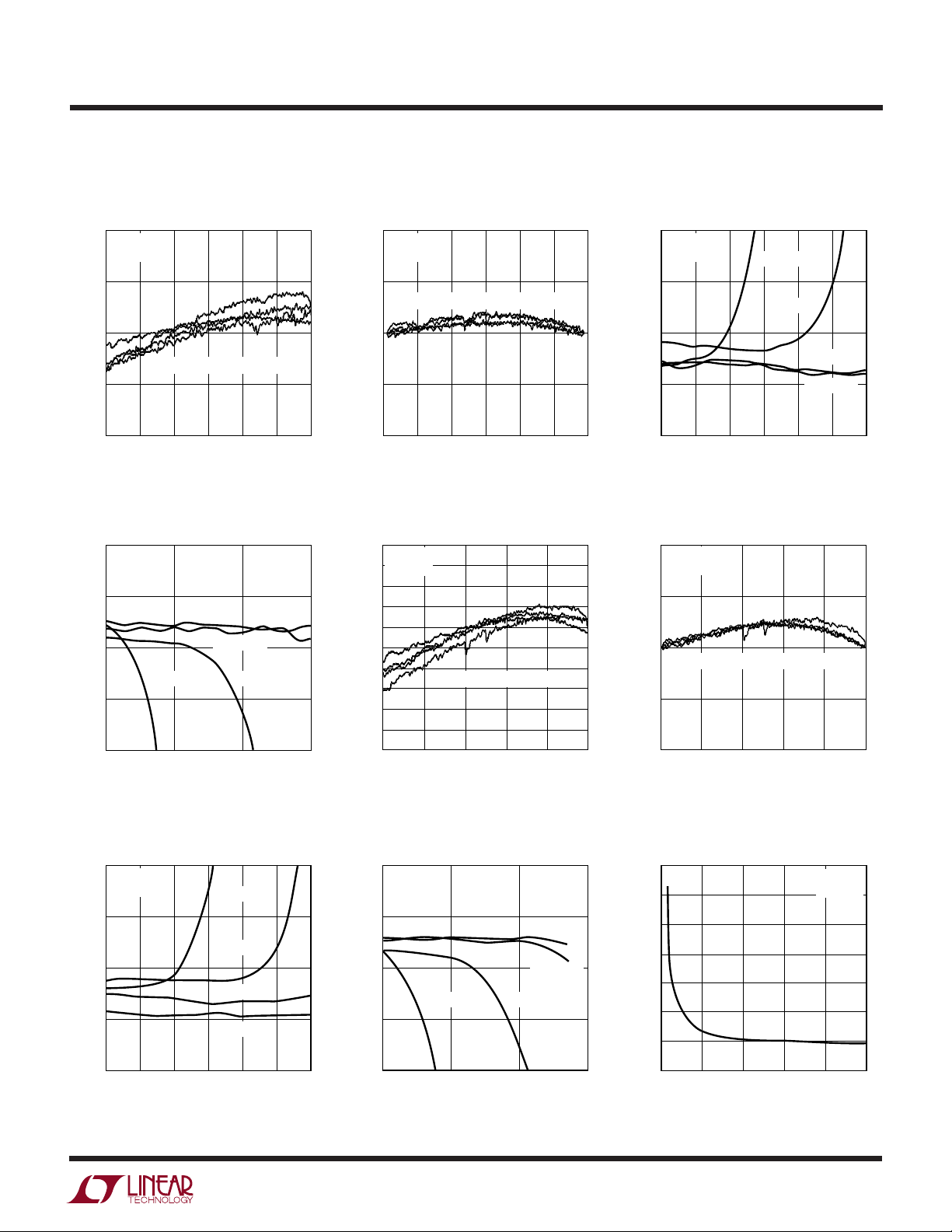
Total Unadjusted Error vs Output Code
10
VCC = 5V
8
= 5V
V
REF
= 25°C
T
A
6
= LOW
F
O
4
2
0
–2
–4
LINEARITY ERROR (ppm)
–6
–8
–10
0 8,338,608 16,777,215
OUTPUT CODE (DECIMAL)
2400 TA02
1
Page 2
LTC2400
WW
W
ABSOLUTE MAXIMUM RATINGS
U
UUW
PACKAGE/ORDER INFORMATION
(Notes 1, 2)
Supply Voltage (VCC) to GND.......................–0.3V to 7V
Analog Input Voltage to GND ....... –0.3V to (VCC + 0.3V)
Reference Input Voltage to GND .. –0.3V to (VCC + 0.3V)
Digital Input Voltage to GND........ –0.3V to (VCC + 0.3V)
Digital Output Voltage to GND ..... –0.3V to (VCC + 0.3V)
Operating Temperature Range
LTC2400C ............................................... 0°C to 70°C
LTC2400I............................................ – 40°C to 85°C
Storage Temperature Range ................. –65°C to 150°C
TOP VIEW
V
1
CC
V
2
REF
V
3
IN
GND
4
S8 PACKAGE
8-LEAD PLASTIC SO
T
= 125°C, θJA = 130°C/W
JMAX
Consult factory for Military grade parts.
8
F
O
SCK
7
SDO
6
CS
5
ORDER PART NUMBER
LTC2400CS8
LTC2400IS8
S8 PART MARKING
2400
2400I
Lead Temperature (Soldering, 10 sec)..................300°C
U
CONVERTER CHARACTERISTICS
temperature range, otherwise specifications are at TA = 25°C. (Notes 3, 4)
PARAMETER CONDITIONS MIN TYP MAX UNITS
Resolution (No Missing Codes) 0.1V ≤ V
Integral Nonlinearity V
Offset Error 2.5V ≤ V
Offset Error Drift 2.5V ≤ V
Full-Scale Error 2.5V ≤ V
Full-Scale Error Drift 2.5V ≤ V
Total Unadjusted Error V
Output Noise VIN = 0V (Note 13) 1.5 µV
Normal Mode Rejection 60Hz ±2% (Note 7) ● 110 130 dB
Normal Mode Rejection 50Hz ±2% (Note 8) ● 110 130 dB
Power Supply Rejection, DC V
Power Supply Rejection, 60Hz ±2% V
Power Supply Rejection, 50Hz ±2% V
REF
V
REF
REF
V
REF
REF
REF
REF
≤ VCC, (Note 5) ● 24 Bits
REF
= 2.5V (Note 6) ● 2 10 ppm of V
= 5V (Note 6) ● 4 15 ppm of V
≤ V
REF
CC
≤ V
REF
CC
≤ V
REF
CC
≤ V
REF
CC
= 2.5V 5 ppm of V
= 5V 10 ppm of V
= 2.5V, VIN = 0V 100 dB
= 2.5V, VIN = 0V, (Notes 7, 15) 110 dB
= 2.5V, VIN = 0V, (Notes 8, 15) 110 dB
The ● denotes specifications which apply over the full operating
● 0.5 2 ppm of V
0.01 ppm of V
● 4 10 ppm of V
0.02 ppm of V
REF
REF
REF
REF
REF
/°C
REF
/°C
REF
REF
RMS
UU
U
A ALOG I PUT A D REFERE CE
U
The ● denotes specifications which apply over the full operating
temperature range, otherwise specifications are at TA = 25°C. (Note 3)
SYMBOL PARAMETER CONDITIONS MIN TYP MAX UNITS
V
IN
V
REF
C
S(IN)
C
S(REF)
I
IN(LEAK)
I
REF(LEAK)
Input Voltage Range (Note 14) ● –0.125 • V
Reference Voltage Range ● 0.1 V
Input Sampling Capacitance 10 pF
Reference Sampling Capacitance 15 pF
Input Leakage Current CS = V
Reference Leakage Current V
= 2.5V, CS = V
REF
CC
CC
● –10 1 10 nA
● –10 1 10 nA
REF
1.125 • V
CC
REF
2
V
V
Page 3
LTC2400
UU
DIGITAL I PUTS A D DIGITAL OUTPUTS
operating temperature range, otherwise specifications are at TA = 25°C. (Note 3)
SYMBOL PARAMETER CONDITIONS MIN TYP MAX UNITS
V
IH
V
IL
V
IH
V
IL
I
IN
I
IN
C
IN
C
IN
V
OH
V
OL
V
OH
V
OL
I
OZ
High Level Input Voltage 2.7V ≤ VCC ≤ 5.5V ● 2.5 V
CS, F
O
Low Level Input Voltage 4.5V ≤ VCC ≤ 5.5V ● 0.8 V
CS, F
O
High Level Input Voltage 2.7V ≤ VCC ≤ 5.5V (Note 9) ● 2.5 V
SCK 2.7V ≤ V
Low Level Input Voltage 4.5V ≤ VCC ≤ 5.5V (Note 9) ● 0.8 V
SCK 2.7V ≤ V
Digital Input Current 0V ≤ VIN ≤ V
CS, F
O
Digital Input Current 0V ≤ VIN ≤ VCC (Note 9) ● –10 10 µA
SCK
Digital Input Capacitance 10 pF
CS, F
O
Digital Input Capacitance (Note 9) 10 pF
SCK
High Level Output Voltage IO = –800µA ● VCC – 0.5V V
SDO
Low Level Output Voltage IO = 1.6mA ● 0.4V V
SDO
High Level Output Voltage IO = –800µA (Note 10) ● VCC – 0.5V V
SCK
Low Level Output Voltage IO = 1.6mA (Note 10) ● 0.4V V
SCK
High-Z Output Leakage ● –10 10 µA
SDO
2.7V ≤ VCC ≤ 3.3V 2.0 V
2.7V ≤ VCC ≤ 5.5V 0.6 V
≤ 3.3V (Note 9) 2.0 V
CC
≤ 5.5V (Note 9) 0.6 V
CC
CC
The ● denotes specifications which apply over the full
● –10 10 µA
WU
POWER REQUIRE E TS
otherwise specifications are at TA = 25°C. (Note 3)
SYMBOL PARAMETER CONDITIONS MIN TYP MAX UNITS
V
CC
I
CC
Supply Voltage ● 2.7 5.5 V
Supply Current
Conversion Mode CS = 0V (Note 12)
Sleep Mode CS = V
The ● denotes specifications which apply over the full operating temperature range,
● 200 300 µA
(Note 12) ● 20 30 µA
CC
3
Page 4
LTC2400
UW
TI I G CHARACTERISTICS
range, otherwise specifications are at TA = 25°C. (Note 3)
SYMBOL PARAMETER CONDITIONS MIN TYP MAX UNITS
f
EOSC
t
HEO
t
LEO
t
CONV
f
ISCK
D
ISCK
f
ESCK
t
LESCK
t
HESCK
t
DOUT_ISCK
t
DOUT_ESCK
t
1
t2 CS ↑ to SDO High Z ● 0 150 ns
t3 CS ↓ to SCK ↓ (Note 10) ● 0 150 ns
t4 CS ↓ to SCK ↑ (Note 9) ● 50 ns
t
KQMAX
t
KQMIN
t
5
t
6
External Oscillator Frequency Range ● 2.56 307.2 kHz
External Oscillator High Period ● 0.5 390 µs
External Oscillator Low Period ● 0.5 390 µs
Conversion Time FO = 0V ● 130.66 133.33 136 ms
Internal SCK Frequency Internal Oscillator (Note 10) 19.2 kHz
Internal SCK Duty Cycle (Note 10) ● 45 55 %
External SCK Frequency Range (Note 9) ● 2000 kHz
External SCK Low Period (Note 9) ● 250 ns
External SCK High Period (Note 9) ● 250 ns
Internal SCK 32-Bit Data Output Time Internal Oscillator (Notes 10, 12) ● 1.64 1.67 1.70 ms
External SCK 32-Bit Data Output Time (Note 9) ● 32/f
CS ↓ to SDO Low Z ● 0 150 ns
SCK ↓ to SDO Valid ● 200 ns
SDO Hold After SCK ↓ (Note 5) ● 15 ns
SCK Set-Up Before CS ↓ ● 50 ns
SCK Hold After CS ↓ ● 50 ns
The ● denotes specifications which apply over the full operating temperature
= V
F
O
CC
External Oscillator (Note 11)
External Oscillator (Notes 10, 11) f
External Oscillator (Notes 10, 11)
● 156.80 160 163.20 ms
● 20480/f
● 256/f
(in kHz) ms
EOSC
/8 kHz
EOSC
(in kHz) ms
EOSC
(in kHz) ms
ESCK
Note 1: Absolute Maximum Ratings are those values beyond which the
life of the device may be impaired.
Note 2: All voltage values are with respect to GND.
Note 3: V
Note 4: Internal Conversion Clock source with the F
to GND or to V
f
EOSC
= 2.7 to 5.5V unless otherwise specified.
CC
or to external conversion clock source with
CC
= 153600Hz unless otherwise specified.
pin tied
O
Note 5: Guaranteed by design, not subject to test.
Note 6: Integral nonlinearity is defined as the deviation of a code from
a straight line passing through the actual endpoints of the transfer
curve. The deviation is measured from the center of the quantization
band.
Note 7: FO = 0V (internal oscillator) or f
= 153600Hz ±2%
EOSC
(external oscillator).
Note 8: F
= VCC (internal oscillator) or f
O
= 128000Hz ±2%
EOSC
(external oscillator).
Note 9: The converter is in external SCK mode of operation such that
the SCK pin is used as digital input. The frequency of the clock signal
driving SCK during the data output is f
and is expressed in kHz.
ESCK
Note 10: The converter is in internal SCK mode of operation such that
the SCK pin is used as digital output. In this mode of operation the
SCK pin has a total equivalent load capacitance C
LOAD
= 20pF.
Note 11: The external oscillator is connected to the FO pin. The external
oscillator frequency, f
, is expressed in kHz.
EOSC
Note 12: The converter uses the internal oscillator.
= 0V or FO = VCC.
F
O
Note 13: The output noise includes the contribution of the internal
calibration operations.
Note 14: For reference voltage values V
of –0.125 • V
to 1.125 • V
REF
is limited by the absolute maximum
REF
rating of the Analog Input Voltage pin (Pin 3). For 2.5V < V
0.267V + 0.89 • V
For 0.267V + 0.89 • V
+ 0.3V.
to V
CC
the input voltage range is –0.3V to 1.125 • V
CC
< V
CC
≤ VCC the input voltage range is –0.3V
REF
> 2.5V the extended input
REF
REF
≤
.
REF
Note 15: The DC voltage at VCC = 4.1V, and the AC voltage applied to
is 2.8V
V
CC
P-P
4
Page 5
UW
REFERENCE VOLTAGE
0
4
5
6
34
2400 G09
3
2
12 5
1
0
–1
OFFSET ERROR (ppm)
VCC = 5V
T
A
= 25°C
TYPICAL PERFOR A CE CHARACTERISTICS
LTC2400
Total Unadjusted Error
(3V Supply) INL (3V Supply)
10
VCC = 3V
= 3V
V
REF
5
0
ERROR (ppm)
–5
–10
0
TA = –55°C, –45°C, 25°C, 90°C
0.5 1.0 1.5 2.0
INPUT VOLTAGE (V)
Positive Input Extended Total
Unadjusted Error (3V Supply)
10
= 3V
V
CC
= 3V
V
REF
5
= –55°C
T
A
0
ERROR (ppm)
–5
–10
3.0
TA = 90°C TA = 25°C
3.1 3.2
INPUT VOLTAGE (V)
TA = –45°C
2.5 3.0
2400 G01
3.3
2400 G04
10
VCC = 3V
= 3V
V
REF
5
0
ERROR (ppm)
–5
–10
0
0.5 1.0 1.5 2.0
Total Unadjusted Error
(5V Supply)
10
VCC = 5V
8
= 5V
V
REF
6
4
2
0
–2
ERROR (ppm)
–4
–6
–8
–10
0
TA = –55°C, –45°C, 25°C, 90°C
INPUT VOLTAGE (V)
TA = –55°C, –45°C, 25°C, 90°C
1
INPUT VOLTAGE (V)
3
2
2.5 3.0
2400 G02
4
2400 G05
5
Negative Input Extended Total
Unadjusted Error (3V Supply)
10
VCC = 3V
= 3V
V
REF
5
0
ERROR (ppm)
–5
–10
–0.050
TA = 90°C
TA = 25°C
INPUT VOLTAGE (V)
INL (5V Supply)
10
VCC = 5V
= 5V
V
REF
5
0
ERROR (ppm)
–5
–10
TA = –55°C, –45°C, 25°C, 90°C
1
0
2
INPUT VOLTAGE (V)
3
TA = –45°C
TA = –55°C
–0.25–0.20–0.15–0.10
2400 G03
4
2400 G06
–0.30
5
10
5
0
ERROR (ppm)
–5
–10
Negative Input Extended Total
Unadjusted Error (5V Supply) Offset Error vs Reference Voltage
VCC = 5V
= 5V
V
REF
–0.050
INPUT VOLTAGE (V)
TA = 90°C
TA = 25°C
TA = –45°C
TA = –55°C
–0.30
–0.25–0.20–0.15–0.10
2400 G07
Positive Input Extended Total
Unadjusted Error (5V Supply)
10
V
= 5V
CC
= 5V
V
REF
5
0
ERROR (ppm)
–5
–10
TA = 90°C TA = 25°C
5.0
5.1 5.2
INPUT VOLTAGE (V)
= –55°C
T
A
TA = –45°C
2400 G08
5.3
5
Page 6
LTC2400
V
CC
2.7
RMS NOISE (ppm)
0
2.5
5.0
3.2 3.7 4.2 4.7
2400 G12
5.2
V
REF
= 2.5V
T
A
= 25°C
V
CC
2.7
0
FULL-SCALE ERROR (ppm)
2
1
3
5
4
6
3.2 3.7 4.2 4.7
2400 G17
5.2
V
REF
= 2.5V
V
IN
= 2.5V
T
A
= 25°C
UW
TYPICAL PERFOR A CE CHARACTERISTICS
RMS Noise vs Reference Voltage Offset Error vs V
20
)
15
REF
10
5
RMS NOISE (ppm OF V
0
1
0
REFERENCE VOLTAGE (V)
VCC = 5V
T
= 25°C
A
3
4
2
5
2400 G10
5.0
V
= 2.5V
REF
= 25°C
T
A
2.5
0
OFFSET ERROR (ppm)
–2.5
–5.0
2.7
RMS Noise vs Code Out
1500
1000
V
= 5V
CC
= 5V
V
REF
= 0V
V
IN
1.00
0.75
0.50
VCC = 5V
= 5V
V
REF
= –0.3V TO 5.3V
V
IN
= 25°C
T
A
CC
3.2 3.7 4.2 4.7
V
CC
5.2
2400 G11
RMS Noise vs V
Offset Error vs TemperatureNoise Histogram
5.0
VCC = 5V
= 5V
V
REF
= 0V
V
IN
2.5
0
CC
500
NUMBER OF READINGS
0
–0.5 0 0.5 1.0
OUTPUT CODE (ppm)
1.5–1.0
2400 G14
RMS NOISE (ppm)
0.25
0
0
7FFFFF
CODE OUT (HEX)
FFFFFF
2400 G18
OFFSET ERROR (ppm)
–2.5
–5.0
–55
–30 –5 20 45
TEMPERATURE (°C)
70 95 120
2400 G13
Full-Scale Error
Full-Scale Error vs Temperature
5.0
2.5
0
–2.5
FULL-SCALE ERROR (ppm)
–5.0
–55
–30 –5 20 45
TEMPERATURE (°C)
VCC = 5V
= 5V
V
REF
= 5V
V
IN
70 95 120
2400 G15
vs Reference Voltage
10.0
7.5
5.0
2.5
FULL-SCALE ERROR (ppm)
0
1
0
REFERENCE VOLTAGE (V)
VCC = 5V
= V
V
IN
REF
3
4
2
5
2400 G16
Full-Scale Error vs V
CC
6
Page 7
UW
FREQUENCY AT VIN (Hz)
1
–120
REJECTION (dB)
–100
–80
–60
–40
–20
0
50 100 150 200
2400 G24
250
VCC = 5V
V
REF
= 5V
V
IN
= 2.5V
F
O
= 0
INPUT FREQUENCY
0
–60
–40
0
2400 F26
–80
–100
fS/2 f
S
–120
–140
–20
REJECTION (dB)
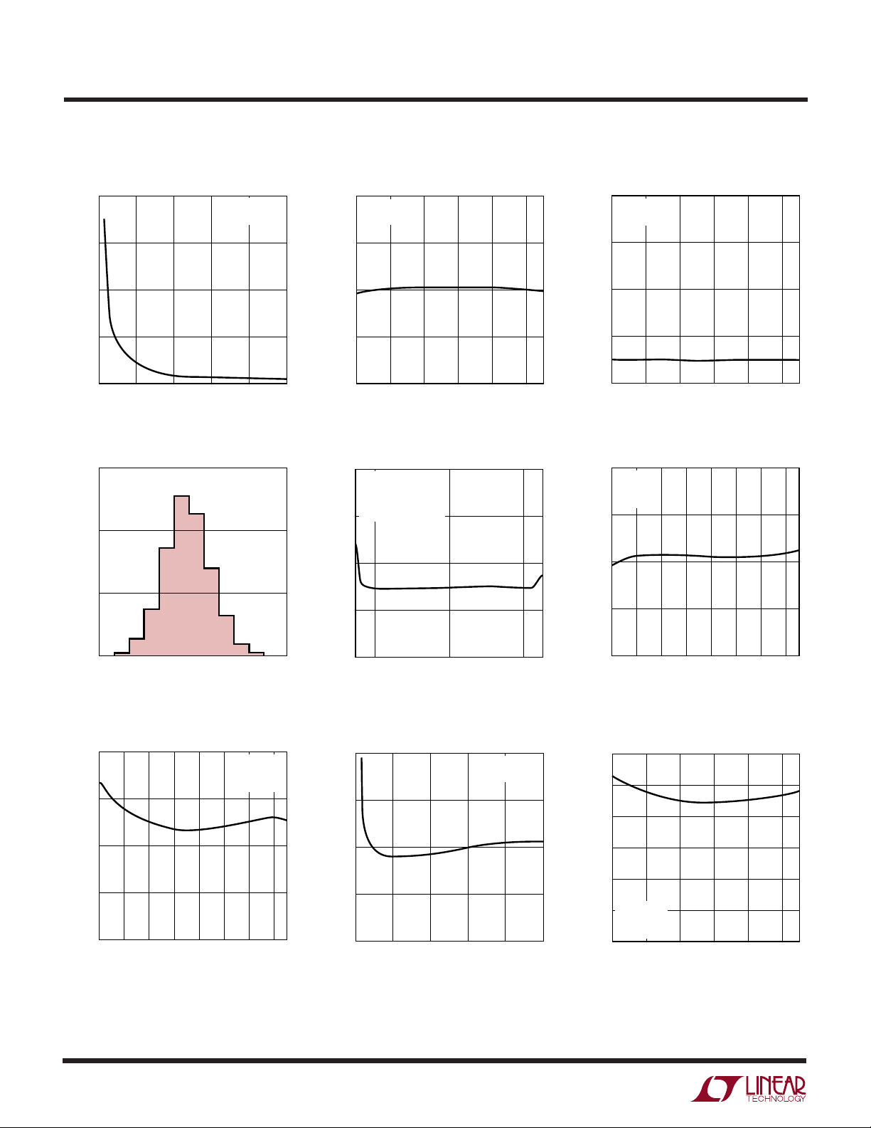
TYPICAL PERFOR A CE CHARACTERISTICS
LTC2400
Conversion Current vs Temperature
230
220
210
200
190
180
SUPPLY CURRENT (µA)
170
160
150
–55
PSRR vs Frequency at V
–10
VCC = 4.1V
V
IN
–30
= 25°C
T
A
= 0
F
0
–50
–70
VCC = 5.5V
VCC = 4.1V
VCC= 2.7V
–30 –5 45
= 0V
20
TEMPERATURE (°C)
70 95 120
CC
2400 G19
Sleep Current vs Temperature
30
25
–30 –5
VCC = 2.7V, 5.5V
45 95 120
20 70
TEMPERATURE (°C)
20
15
10
SUPPLY CURRENT (µA)
5
0
–55
PSRR vs Frequency at V
0
VCC = 4.1V
= 0V
V
IN
–20
= 25°C
T
A
= 0
F
O
–40
–60
CC
2400 G20
PSRR vs Frequency at V
0
VCC = 4.1V
= 0V
V
IN
–20
= 25°C
T
A
= 0
F
O
–40
–60
REJECTION (dB)
–80
–100
–120
1
15,360Hz 153,600Hz
100 10k 1M
FREQUENCY AT VCC (Hz)
Rejection vs Frequency at V
CC
2400 G23
IN
REJECTION (dB)
–90
–110
–130
0
50 100 150 200
FREQUENCY AT VCC (Hz)
Rejection vs Frequency at V
–60
–70
–80
–90
–100
–110
REJECTION (dB)
–120
–130
–140
–12–8–404812
INPUT FREQUENCY DEVIATION FROM NOTCH FREQUENCY (%)
250
2400 G21
IN
2400 G25
REJECTION (dB)
–80
–100
–120
15200
15300 15350 15400
15250
FREQUENCY AT VCC (Hz)
Rejection vs Frequency at V
0
VCC = 5V
= 5V
V
REF
–20
= 2.5V
V
IN
= 0
F
O
–40
–60
REJECTION (dB)
–80
–100
–120
SAMPLE RATE = 15.36kHz ±2%
15100
15200 15300 15400 15500
FREQUENCY AT VIN (Hz)
15450 15500
1635 G22
IN
2400 G26
Rejection vs Frequency at V
IN
7
Page 8
LTC2400
UW
TYPICAL PERFOR A CE CHARACTERISTICS
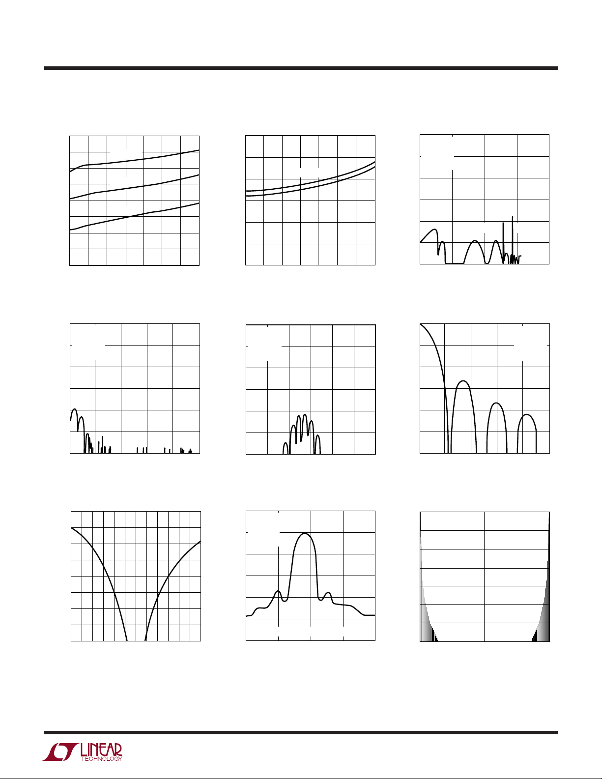
INL vs Output Rate Resolution vs Output Rate
24
22
20
18
16
INL (BITS)
14
12
10
8
0
VCC = 5V
= 5V
V
REF
= 25°C
T
A
F
= EXTERNAL
0
15 20 25105 303540455055
OUTPUT RATE (Hz)
2400 G27
60
24
22
20
18
16
14
RESOLUTION (BITS)*
12
10
8
UUU
PIN FUNCTIONS
*RESOLUTION =
0
15 20 25105 303540455055
VCC = 5V
V
T
F
/RMS NOISE)
LOG(V
REF
LOG (2)
OUTPUT RATE (Hz)
= 5V
REF
= 25°C
A
= EXTERNAL
O
2400 G28
60
VCC (Pin 1): Positive Supply Voltage. Bypass to GND
(Pin␣ 4) with a 10µF tantalum capacitor in parallel with
0.1µF ceramic capacitor as close to the part as possible.
V
(Pin 2): Reference Input. The reference voltage range
REF
is 0.1V to VCC.
VIN (Pin 3): Analog Input. The input voltage range is
–0.125 • V
to 1.125 • V
REF
REF
. For V
> 2.5V, the input
REF
voltage range may be limited by the pin absolute maximum rating of –0.3V to VCC + 0.3V.
GND (Pin 4): Ground. Shared pin for analog ground,
digital ground, reference ground and signal ground. Should
be connected directly to a ground plane through a minimum length trace or it should be the single-point-ground
in a single point grounding system.
CS (Pin 5): Active LOW Digital Input. A LOW on this pin
enables the SDO digital output and wakes up the ADC.
Following each conversion the ADC automatically enters
the Sleep mode and remains in this low power state as
long as CS is HIGH. A LOW on CS wakes up the ADC. A
LOW-to-HIGH transition on this pin disables the SDO
digital output. A LOW-to-HIGH transition on CS during the
Data Output transfer aborts the data transfer and starts a
new conversion.
SDO (Pin 6): Three-State Digital Output. During the data
output period, this pin is used for serial data output. When
the chip select CS is HIGH (CS = VCC), the SDO pin is in a
high impedance state. During the Conversion and Sleep
periods this pin can be used as a conversion status output.
The conversion status can be observed by pulling CS LOW.
SCK (Pin 7): Bidirectional Digital Clock Pin. In Internal
Serial Clock Operation mode, SCK is used as digital output
for the internal serial interface clock during the data output
period. In External Serial Clock Operation mode, SCK is
used as digital input for the external serial interface. A
weak internal pull-up is automatically activated in Internal
Serial Clock Operation mode. The Serial Clock mode is
determined by the level applied to SCK at power up and the
falling edge of CS.
FO (Pin 8): Frequency Control Pin. Digital input that
controls the ADC’s notch frequencies and conversion
time. When the FO pin is connected to VCC (FO = VCC), the
converter uses its internal oscillator and the digital filter
first null is located at 50Hz. When the FO pin is connected
to GND (FO = OV), the converter uses its internal oscillator
and the digital filter first null is located at 60Hz. When F
is driven by an external clock signal with a frequency f
O
EOSC,
the converter uses this signal as its clock and the digital
filter first null is located at a frequency f
EOSC
/2560.
8
Page 9

LTC2400
3.4k
SDO
2400 TA04
HI-Z TO V
OL
VOH TO V
OL
VOL TO HI-Z
C
LOAD
= 20pF
V
CC
CONVERT
SLEEP
DATA OUTPUT
2400 F01
0
1
CS AND
SCK
UU
W
FU CTIO AL BLOCK DIAGRA
V
CC
GND
V
IN
V
REF
DAC
∫∫∫
∑
ADC
AUTOCALIBRATION
AND CONTROL
DECIMATING FIR
INTERNAL
OSCILLATOR
SERIAL
INTERFACE
(INT/EXT)
F
O
SDO
SCK
CS
2400 FD
TEST CIRCUITS
SDO
3.4k
HI-Z TO V
VOL TO V
OH
VOH TO HI-Z
U
OH
= 20pF
C
LOAD
2400 TA03
WUU
APPLICATIONS INFORMATION
Converter Operation Cycle
The LTC2400 is a low power, delta-sigma analog-todigital converter with an easy to use 3-wire serial interface.
Its operation is simple and made up of three states. The
converter operating cycle begins with the conversion,
followed by a low power sleep state and concluded with
the data output (see Figure 1). The 3-wire interface consists of serial data output (SDO), a serial clock (SCK) and
a chip select (CS).
Initially, the LTC2400 performs a conversion. Once the
conversion is complete, the device enters the sleep state.
While in this sleep state, power consumption is reduced by
Figure 1. LTC2400 State Transition Diagram
9
Page 10

LTC2400
U
WUU
APPLICATIONS INFORMATION
an order of magnitude. The part remains in the sleep state
as long as CS is logic HIGH. The conversion result is held
indefinitely in a static shift register while the converter is
in the sleep state.
Once CS is pulled low, the device begins outputting the
conversion result. There is no latency in the conversion
result. The data output corresponds to the conversion just
performed. This result is shifted out on the serial data out
pin (SDO) under the control of the serial clock (SCK). Data
is updated on the falling edge of SCK allowing the user to
reliably latch data on the rising edge of SCK, see Figure 3.
The data output state is concluded once 32 bits are read
out of the ADC or when CS is brought HIGH. The device
automatically initiates a new conversion cycle and the
cycle repeats.
Through timing control of the CS and SCK pins, the
LTC2400 offers several flexible modes of operation
(internal or external SCK and free-running conversion
modes). These various modes do not require programming configuration registers; moreover, they do not disturb the cyclic operation described above. These modes of
operation are described in detail in the Serial Interface
Timing Modes section.
Conversion Clock
A major advantage delta-sigma converters offer over
conventional type converters is an on-chip digital filter
(commonly known as Sinc or Comb filter). For high
resolution, low frequency applications, this filter is typically designed to reject line frequencies of 50 or 60Hz plus
their harmonics. In order to reject these frequencies in
excess of 110dB, a highly accurate conversion clock is
required. The LTC2400 incorporates an on-chip highly
accurate oscillator. This eliminates the need for external
frequency setting components such as crystals or oscillators. Clocked by the on-chip oscillator, the LTC2400
rejects line frequencies (50 or 60Hz ±2%) a minimum of
110dB.
conversion and the output data. Therefore, multiplexing
an analog input voltage is easy.
The LTC2400 performs offset and full-scale calibrations
every conversion cycle. This calibration is transparent to
the user and has no effect on the cyclic operation described above. The advantage of continuous calibration is
extreme stability of offset and full-scale readings with respect to time, supply voltage change and temperature drift.
Power-Up Sequence
The LTC2400 automatically enters an internal reset state
when the power supply voltage VCC drops below approximately 2.2V. This feature guarantees the integrity of the
conversion result and of the serial interface mode selection which is performed at the initial power-up. (See the
2-wire I/O sections in the Serial Interface Timing Modes
section.)
When the VCC voltage rises above this critical threshold,
the converter creates an internal power-on-reset (POR)
signal with duration of approximately 0.5ms. The POR
signal clears all internal registers. Following the POR
signal, the LTC2400 starts a normal conversion cycle and
follows the normal succession of states described above.
The first conversion result following POR is accurate
within the specifications of the device.
Reference Voltage Range
The LTC2400 can accept a reference voltage from 0V to
VCC. The converter output noise is determined by the
thermal noise of the front-end circuits, and as such, its
value in microvolts is nearly constant with reference
voltage. A decrease in reference voltage will not significantly improve the converter’s effective resolution. On the
other hand, a reduced reference voltage will improve the
overall converter INL performance. The recommended
range for the LTC2400 voltage reference is 100mV to VCC.
Input Voltage Range
Ease of Use
The LTC2400 data output has no latency, filter settling or
redundant data associated with the conversion cycle.
There is a one-to-one correspondence between the
10
The converter is able to accommodate system level offset
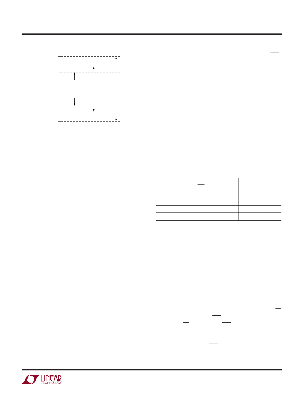
and gain errors as well as system level overrange situations due to its extended input range, see Figure 2. The
LTC2400 converts input signals within the extended input
range of –0.125 • V
to 1.125 • V
REF
REF
.
Page 11
LTC2400
U
WUU
APPLICATIONS INFORMATION
VCC + 0.3V
9/8V
REF
V
REF
NORMAL
1/2V
–1/8V
REF
0
REF
–0.3V
INPUT
RANGE
Figure 2. LTC2400 Input Range
For large values of V
EXTENDED
INPUT
RANGE
this range is limited by the
REF
absolute maximum voltage range of – 0.3V to (VCC + 0.3V).
Beyond this range the input ESD protection devices begin
to turn on and the errors due to the input leakage current
increase rapidly.
Input signals applied to VIN may extend below ground by
–300mV and above VCC by 300mV. In order to limit any
fault current, a resistor of up to 5k may be added in series
with the VIN pin without affecting the performance of the
device. In the physical layout, it is important to maintain
the parasitic capacitance of the connection between this
series resistance and the VIN pin as low as possible;
therefore, the resistor should be located as close as
practical to the VIN pin. The effect of the series resistance
on the converter accuracy can be evaluated from the
curves presented in the Analog Input/Reference Current
section. In addition a series resistor will introduce a
temperature dependent offset error due to the input leakage current. A 1nA input leakage current will develop a
1ppm offset error on a 5k resistor if V
has a very strong temperature dependency.
Output Data Format
The LTC2400 serial output data stream is 32 bits long. The
first 4 bits represent status information indicating the
sign, input range and conversion state. The next 24 bits are
the conversion result, MSB first. The remaining 4 bits are
sub LSBs beyond the 24-bit level that may be included in
averaging or discarded without loss of resolution.
ABSOLUTE
MAXIMUM
INPUT
RANGE
2400 F02
= 5V. This error
REF
Bit 31 (first output bit) is the end of conversion (EOC)
indicator. This bit is available at the SDO pin during the
conversion and sleep states whenever the CS pin is LOW.
This bit is HIGH during the conversion and goes LOW
when the conversion is complete.
Bit 30 (second output bit) is a dummy bit (DMY) and is
always LOW.
Bit 29 (third output bit) is the conversion result sign indicator (SIG). If VIN is >0, this bit is HIGH. If VIN is <0, this
bit is LOW. The sign bit changes state during the zero code.
Bit 28 (forth output bit) is the extended input range (EXR)
indicator. If the input is within the normal input range
0␣ ≤␣VIN ≤ V
normal input range, VIN > V
, this bit is LOW. If the input is outside the
REF
or VIN < 0, this bit is HIGH.
REF
The function of these bits is summarized in Table 1.
Table 1. LTC2400 Status Bits
Bit 31 Bit 30 Bit 29 Bit 28
Input Range EOC DMY SIG EXR
VIN > V
REF
0 < VIN ≤ V
VIN = 0+/0
VIN < 0 0 001
REF
–
0 011
0 010
0 0 1/0 0
Bit 27 (fifth output bit) is the most significant bit (MSB).
Bits 27-4 are the 24-bit conversion result MSB first.
Bit 4 is the least significant bit (LSB).
Bits 3-0 are sub LSBs below the 24-bit level. Bits 3-0 may
be included in averaging or discarded without loss of
resolution.
Data is shifted out of the SDO pin under control of the serial
clock (SCK), see Figure 3. Whenever CS is HIGH, SDO
remains high impedance and any SCK clock pulses are
ignored by the internal data out shift register.
In order to shift the conversion result out of the device, CS
must first be driven LOW. EOC is seen at the SDO pin of the
device once CS is pulled LOW. EOC changes real time from
HIGH to LOW at the completion of a conversion. This
signal may be used as an interrupt for an external
microcontroller. Bit 31 (EOC) can be captured on the first
rising edge of SCK. Bit 30 is shifted out of the device on the
first falling edge of SCK. The final data bit (Bit 0) is shifted
11
Page 12
LTC2400
U
WUU
APPLICATIONS INFORMATION
out on the falling edge of the 31st SCK and may be latched
on the rising edge of the 32nd SCK pulse. On the falling
edge of the 32nd SCK pulse, SDO goes HIGH indicating a
new conversion cycle has been initiated. This bit serves as
EOC (Bit 31) for the next conversion cycle. Table 2 summarizes the output data format.
As long as the voltage on the VIN pin is maintained within
the –0.3V to (VCC + 0.3V) absolute maximum operating
range, a conversion result is generated for any input value
from –0.125 • V
greater than 1.125 • V
SDO
to 1.125 • V
REF
REF
CS
Hi-Z
For input voltages
REF.
, the conversion result is clamped
BIT 31
EOC
BIT 28BIT 29BIT 30
to the value corresponding to 1.125 • V
voltages below –0.125 • V
, the conversion result is
REF
clamped to the value corresponding to –0.125 • V
. For input
REF
REF
.
Frequency Rejection Selection (FO Pin Connection)
The LTC2400 internal oscillator provides better than 110dB
normal mode rejection at the line frequency and all its
harmonics for 50Hz ±2% or 60Hz ±2%. For 60Hz rejection, FO (Pin 8) should be connected to GND (Pin 4) while
for 50Hz rejection the FO pin should be connected to V
CC
(Pin␣ 1).
BIT 0BIT 27 BIT 4
MSBEXTSIG“0”
LSB
24
SCK
SLEEP DATA OUTPUT CONVERSION
1 2 3 4 5 272832
2400 F03
Figure 3. Output Data Timing
Table 2. LTC2400 Output Data Format
Bit 31 Bit 30 Bit 29 Bit 28 Bit 27 Bit 26 Bit 25 Bit 24 Bit 23 … Bit 4 Bit 3-0
Input Voltage EOC DMY SIG EXR MSB LSB SUB LSBs*
VIN > 9/8 • V
9/8 • V
V
REF
V
REF
3/4V
3/4V
1/2V
1/2V
1/4V
1/4V
0+/0
–1LSB 0 0 0111 1 11...1 X
–1/8 • V
VIN < –1/8 • V
*The sub LSBs are valid conversion results beyond the 24-bit level that may be included in averaging or discarded without loss of resolution.
**The sign bit changes state during the 0 code.
REF
REF
+ 1LSB 0 0 1 1 0 0 0 0 0 ... 0 X
+ 1LSB 0 0 1 0 1 1 0 0 0 ... 0 X
REF
REF
+ 1LSB 0 0 1 0 1 0 0 0 0 ... 0 X
REF
REF
+ 1LSB 0 0 1 0 0 1 0 0 0 ... 0 X
REF
REF
–
REF
REF
001100011...1X
001100011...1X
001011111...1X
001010111...1X
001001111...1X
001000111...1X
0 0 1/0** 0 0 0 0 0 0 ... 0 X
000111100...0X
000111100...0X
12
Page 13

LTC2400
U
WUU
APPLICATIONS INFORMATION
The selection of 50Hz or 60Hz rejection can also be made
by driving FO to an appropriate logic level. A selection
change during the sleep or data output states will not
disturb the converter operation. If the selection is made
during the conversion state, the result of the conversion in
progress may be outside specifications but the following
conversions will not be affected.
When a fundamental rejection frequency different from
50Hz or 60Hz is required or when the converter must be
synchronized with an outside source, the LTC2400 can
operate with an external conversion clock. The converter
automatically detects the presence of an external clock
signal at the FO pin and turns off the internal oscillator. The
frequency f
2560Hz (1Hz notch frequency) to be detected. The external clock signal duty cycle is not significant as long as the
minimum and maximum specifications for the high and
low periods t
While operating with an external conversion clock of a
frequency f
normal mode rejection in a frequency range f
±4% and its harmonics. The normal mode rejection as a
function of the input frequency deviation from f
is shown in Figure 4.
Whenever an external clock is not present at the FO pin, the
converter automatically activates its internal oscillator and
enters the Internal Conversion Clock mode. The LTC2400
of the external signal must be at least
EOSC
and t
HEO
, the LTC2400 provides better than 110dB
EOSC
are observed.
LEO
EOSC
EOSC
/2560
/2560
–60
–70
–80
–90
–100
–110
REJECTION (dB)
–120
–130
–140
–12–8–404812
INPUT FREQUENCY DEVIATION FROM NOTCH FREQUENCY (%)
2400 G25
Figure 4. LTC2400 Normal Mode Rejection When
Using an External Oscillator of Frequency f
EOSC
operation will not be disturbed if the change of conversion
clock source occurs during the sleep state or during the
data output state while the converter uses an external
serial clock. If the change occurs during the conversion
state, the result of the conversion in progress may be
outside specifications but the following conversions will
not be affected. If the change occurs during the data output
state and the converter is in the Internal SCK mode, the
serial clock duty cycle may be affected but the serial data
stream will remain valid.
Table 3 summarizes the duration of each state as a
function of FO.
Table 3. LTC2400 State Duration
State Operating Mode Duration
CONVERT Internal Oscillator FO = LOW 133ms
(60Hz Rejection)
FO = HIGH 160ms
(50Hz Rejection)
External Oscillator FO = External Oscillator 20480/f
with Frequency f
/2560 Rejection)
(f
EOSC
SLEEP As Long As CS = HIGH Until CS = 0 and SCK
DATA OUTPUT Internal Serial Clock FO = LOW/HIGH As Long As CS = LOW But Not Longer Than 1.67ms
(Internal Oscillator) (32 SCK cycles)
FO = External Oscillator with As Long As CS = LOW But Not Longer Than 256/f
Frequency f
External Serial Clock with As Long As CS = LOW But Not Longer Than 32/f
Frequency f
kHz (32 SCK cycles)
SCK
EOSC
kHz
EOSC
kHz (32 SCK cycles)
EOSC
s
EOSC
ms
SCK
ms
13
Page 14

LTC2400
U
WUU
APPLICATIONS INFORMATION
SERIAL INTERFACE
The LTC2400 transmits the conversion results and receives the start of conversion command through a synchronous 3-wire interface. During the conversion and
sleep states, this interface can be used to assess the
converter status and during the data output state it is used
to read the conversion result.
Serial Clock Input/Output (SCK)
The serial clock signal present on SCK (Pin 7) is used to
synchronize the data transfer. Each bit of data is shifted out
the SDO pin on the falling edge of the serial clock.
In the Internal SCK mode of operation, the SCK pin is an
output and the LTC2400 creates its own serial clock by
dividing the internal conversion clock by 8. In the External
SCK mode of operation, the SCK pin is used as input. The
internal or external SCK mode is selected on power-up and
then reselected every time a HIGH-to-LOW transition is
detected at the CS pin. If SCK is HIGH or floating at powerup or during this transition, the converter enters the internal SCK mode. If SCK is LOW at power-up or during this
transition, the converter enters the external SCK mode.
the SDO pin. Once the conversion is complete, EOC goes
LOW. The device remains in the sleep state until the first
rising edge of SCK occurs while CS = 0.
Chip Select Input (CS)
The active LOW chip select, CS (Pin 5), is used to test the
conversion status and to enable the data output transfer as
described in the previous sections.
In addition, the CS signal can be used to trigger a new
conversion cycle before the entire serial data transfer has
been completed. The LTC2400 will abort any serial data
transfer in progress and start a new conversion cycle
anytime a LOW-to-HIGH transition is detected at the CS
pin after the converter has entered the data output state
(i.e., after the first rising edge of SCK occurs with CS = 0).
Finally, CS can be used to control the free-running modes
of operation, see Serial Interface Timing Modes section.
Grounding CS will force the ADC to continuously convert
at the maximum output rate selected by FO. Tying a
capacitor to CS will reduce the output rate and power
dissipation by a factor proportional to the capacitor’s
value, see Figures 12 to 14.
Serial Data Output (SDO)
The serial data output pin, SDO (Pin 6), drives the serial
data during the data output state. In addition, the SDO pin
is used as an end of conversion indicator during the
conversion and sleep states.
When CS (Pin 5) is HIGH, the SDO driver is switched to a
high impedance state. This allows sharing the serial
interface with other devices. If CS is LOW during the
convert or sleep state, SDO will output EOC. If CS is LOW
during the conversion phase, the EOC bit appears HIGH on
Table 4. LTC2400 Interface Timing Modes
SCK Cycle Output and
Configuration Source Control Control Waveforms
External SCK, Single Cycle Conversion External CS and SCK CS and SCK Figures 5, 6
External SCK, 2-Wire I/O External SCK SCK Figure 7
Internal SCK, Single Cycle Conversion Internal CS ↓ CS ↓ Figures 8, 9
Internal SCK, 2-Wire I/O, Continuous Conversion Internal Continuous Internal Figure 10
Internal SCK, Autostart Conversion Internal C
SERIAL INTERFACE TIMING MODES
The LTC2400’s 3-wire interface is SPI and MICROWIRE
compatible. This interface offers several flexible modes of
operation. These include internal/external serial clock,
2- or 3-wire I/O, single cycle conversion and autostart. The
following sections describe each of these serial interface
timing modes in detail. In all these cases, the converter
can use the internal oscillator (FO = LOW or FO = HIGH) or
an external oscillator connected to the FO pin. Refer to
Table 4 for a summary.
Conversion Data Connection
EXT
Internal Figure 11
14
Page 15

LTC2400
U
WUU
APPLICATIONS INFORMATION
External Serial Clock, Single Cycle Operation
(SPI/MICROWIRE Compatible)
This timing mode uses an external serial clock to shift out
the conversion result and a CS signal to monitor and
control the state of the conversion cycle, see Figure 5.
The serial clock mode is selected on the falling edge of CS.
To select the external serial clock mode, the serial clock pin
(SCK) must be LOW during each CS falling edge.
The serial data output pin (SDO) is HI-Z as long as CS is
HIGH. At any time during the conversion cycle, CS may be
pulled LOW in order to monitor the state of the converter.
While CS is pulled LOW, EOC is output to the SDO pin. EOC
= 1 while a conversion is in progress and EOC = 0 if the
device is in the sleep state. Independent of CS, the device
automatically enters the low power sleep state once the
conversion is complete.
When the device is in the sleep state (EOC = 0), its
conversion result is held in an internal static shift register. The device remains in the sleep state until the first
rising edge of SCK is seen while CS is LOW. Data is
shifted
out the SDO pin on each falling edge of SCK. This enables
external circuitry to latch the output on the rising edge of
SCK. EOC can be latched on the first rising edge of SCK
and the last bit of the conversion result can be latched on
the 32nd rising edge of SCK. On the 32nd falling edge of
SCK, the device begins a new conversion. SDO goes HIGH
(EOC = 1) indicating a conversion is in progress.
At the conclusion of the data cycle, CS may remain LOW
and EOC monitored as an end-of-conversion interrupt.
Alternatively, CS may be driven HIGH setting SDO to HI-Z.
As described above, CS may be pulled LOW at any time in
order to monitor the conversion status.
Typically, CS remains LOW during the data output state.
However, the data output state may be aborted by pulling
CS HIGH anytime between the first rising edge and the
32nd falling edge of SCK, see Figure 6. On the rising edge
of CS, the device aborts the data output state and immediately initiates a new conversion. This is useful for systems not requiring all 32 bits of output data, aborting an
invalid conversion cycle or synchronizing the start of a
conversion.
SDO
SCK
(EXTERNAL)
CS
CONVERSION
2.7V TO 5.5V
1µF
V
V
REF
V
REF
CC
IN
V
V
GND CS
0.1V TO V
–0.12V
TO 1.12V
REF
TEST EOCTEST EOC
SLEEP DATA OUTPUT CONVERSION
BIT 31
EOC
CC
LTC2400
REF
IN
F
O
SCK
SDO
MSB SUB LSBEXRSIG
V
CC
= 50Hz REJECTION
= EXTERNAL OSCILLATOR
= 60Hz REJECTION
BIT 4BIT 27 BIT 26BIT 28BIT 29BIT 30
LSB
BIT 0
Figure 5. External Serial Clock, Single Cycle Operation
TEST EOC
Hi-ZHi-ZHi-Z
2400 F05
15
Page 16

LTC2400
U
WUU
APPLICATIONS INFORMATION
–0.12V
TO 1.12V
REF
CS
TEST EOC TEST EOC
SDO
SCK
(EXTERNAL)
EOC
CONVERSIONSLEEP SLEEP
DATA OUTPUT
Hi-Z
Hi-Z Hi-ZHi-Z
2.7V TO 5.5V
1µF
0.1V TO V
BIT 31BIT 0
EOC
V
CC
= 50Hz REJECTION
V
V
REF
V
CC
V
IN
V
REF
GND CS
CC
LTC2400
REF
IN
F
SCK
SDO
O
DATA OUTPUT
= EXTERNAL OSCILLATOR
= 60Hz REJECTION
MSBEXRSIG
BIT 8BIT 27 BIT 9BIT 28BIT 29BIT 30
TEST EOC
CONVERSION
2400 F06
Figure 6. External Serial Clock, Reduced Data Output Length
External Serial Clock, 2-Wire I/O
This timing mode utilizes a 2-wire serial I/O interface. The
conversion result is shifted out of the device by an externally generated serial clock (SCK) signal, see Figure 7. CS
may be permanently tied to ground (Pin 4), simplifying the
user interface or isolation barrier.
The external serial clock mode is selected at the end of the
power-on reset (POR) cycle. The POR cycle is concluded
approximately 0.5ms after VCC exceeds 2.2V. The level
applied to SCK at this time determines if SCK is internal or
external. SCK must be driven LOW prior to the end of POR
in order to enter the external serial clock timing mode.
Since CS is tied LOW, the end-of-conversion (EOC) can be
continuously monitored at the SDO pin during the convert
and sleep states. EOC may be used as an interrupt to an
external controller indicating the conversion result is
ready. EOC = 1 while the conversion is in progress and EOC
= 0 once the conversion enters the low power sleep state.
On the falling edge of EOC, the conversion result is loaded
into an internal static shift register. The device remains in
the sleep state until the first rising edge of SCK. Data is
shifted out the SDO pin on each falling edge of SCK
enabling external circuitry to latch data on the rising edge
of SCK. EOC can be latched on the first rising edge of SCK.
On the 32nd falling edge of SCK, SDO goes HIGH (EOC =
1) indicating a new conversion has begun.
Internal Serial Clock, Single Cycle Operation
This timing mode uses an internal serial clock to shift out
the conversion result and a CS signal to monitor and
control the state of the conversion cycle, see Figure 8.
In order to select the internal serial clock timing mode, the
serial clock pin (SCK) must be floating (HI-Z) or pulled
HIGH prior to the falling edge of CS. The device will not
enter the internal serial clock mode if SCK is driven LOW
on the falling edge of CS. An internal weak pull-up resistor
is active on the SCK pin during the falling edge of CS;
therefore, the internal serial clock timing mode is automatically selected if SCK is not externally driven.
The serial data output pin (SDO) is HI-Z as long as CS is
HIGH. At any time during the conversion cycle, CS may be
pulled LOW in order to monitor the state of the converter.
16
Page 17

LTC2400
U
WUU
APPLICATIONS INFORMATION
–0.12V
TO 1.12V
REF
CS
BIT 31
SDO
SCK
(EXTERNAL)
CONVERSION
SLEEP DATA OUTPUT CONVERSION
EOC
1µF
0.1V TO V
2.7V TO 5.5V
V
REF
CC
V
IN
REF
V
CC
LTC2400
V
SCK
REF
SDO
V
IN
GND CS
MSBEXRSIG
V
CC
= 50Hz REJECTION
F
O
= EXTERNAL OSCILLATOR
= 60Hz REJECTION
BIT 4BIT 27 BIT 26BIT 28BIT 29BIT 30
LSB
24
BIT 0
2400 F07
SDO
SCK
(INTERNAL)
Figure 7. External Serial Clock, CS = 0 Operation
2.7V TO 5.5V
1µF
V
V
REF
V
REF
CC
IN
V
V
GND CS
0.1V TO V
–0.12V
TO 1.12V
REF
<t
EOCtest
CS
TEST EOC
Hi-Z Hi-Z Hi-Z Hi-Z
BIT 31
EOC
SLEEP DATA OUTPUT CONVERSIONCONVERSION
CC
LTC2400
REF
IN
F
O
SCK
SDO
BIT 27 BIT 26BIT 28BIT 29BIT 30
MSBEXRSIG
V
CC
= 50Hz REJECTION
= EXTERNAL OSCILLATOR
= 60Hz REJECTION
BIT 4
LSB
24
V
CC
10k
BIT 0
TEST EOC
2400 F08
Figure 8. Internal Serial Clock, Single Cycle Operation
17
Page 18

LTC2400
U
WUU
APPLICATIONS INFORMATION
Once CS is pulled LOW, SCK goes LOW and EOC is output
to the SDO pin. EOC = 1 while a conversion is in progress
and EOC = 0 if the device is in the sleep state.
When testing EOC, if the conversion is complete (EOC = 0),
the device will exit the sleep state and enter the data output
state if CS remains LOW. In order to prevent the device
from exiting the low power sleep state, CS must be pulled
HIGH before the first rising edge of SCK. In the internal
SCK timing mode, SCK goes HIGH and the device begins
outputting data at time t
(if EOC = 0) or t
after EOC goes LOW (if CS is LOW
EOCtest
during the falling edge of EOC). The value of t
if the device is using its internal oscillator (F0 = logic LOW
or HIGH). If FO is driven by an external oscillator of
frequency f
HIGH before time t
EOSC
, then t
EOCtest
EOCtest
state. The conversion result is held in the internal static
shift register.
If CS remains LOW longer than t
edge of SCK will occur and the conversion result is serially
after the falling edge of CS
EOCtest
is 23µs
EOCtest
is 3.6/f
. If CS is pulled
EOSC
, the device remains in the sleep
, the first rising
EOCtest
shifted out of the SDO pin. The data output cycle begins on
this first rising edge of SCK and concludes after the 32nd
rising edge. Data is shifted out the SDO pin on each falling
edge of SCK. The internally generated serial clock is output
to the SCK pin. This signal may be used to shift the
conversion result into external circuitry. EOC can be
latched on the first rising edge of SCK and the last bit of the
conversion result on the 32nd rising edge of SCK. After the
32nd rising edge, SDO goes HIGH (EOC = 1), SCK stays
HIGH, and a new conversion starts.
Typically, CS remains LOW during the data output state.
However, the data output state may be aborted by pulling
CS HIGH anytime between the first and 32nd rising edge
of SCK, see Figure 9. On the rising edge of CS, the device
aborts the data output state and immediately initiates a
new conversion. This is useful for systems not requiring
all 32 bits of output data, aborting an invalid conversion
cycle, or synchronizing the start of a conversion. If CS is
pulled HIGH while the converter is driving SCK LOW, the
internal pull-up is not available to restore SCK to a logic
SDO
SCK
(INTERNAL)
2.7V TO 5.5V
1µF
V
V
REF
V
REF
CC
IN
V
V
GND CS
0.1V TO V
–0.12V
TO 1.12V
REF
>t
EOCtest
CS
BIT 0
EOC
Hi-Z Hi-Z Hi-Z Hi-Z Hi-Z
DATA OUTPUT
TEST EOCTEST EOC
<t
EOCtest
BIT 31
EOC
SLEEP DATA OUTPUT
CC
LTC2400
REF
IN
SCK
SDO
F
O
V
CC
= 50Hz REJECTION
= EXTERNAL OSCILLATOR
= 60Hz REJECTION
BIT 27 BIT 26BIT 28BIT 29BIT 30
MSBEXRSIG
BIT 8
V
CC
10k
TEST EOC
CONVERSIONCONVERSIONSLEEP
2400 F09
18
Figure 9. Internal Serial Clock, Reduced Data Output Length
Page 19

LTC2400
U
WUU
APPLICATIONS INFORMATION
HIGH state. This will cause the device to exit the internal
serial clock mode on the next falling edge of CS. This can
be avoided by adding an external 10k pull-up resistor to
the SCK pin or by never pulling CS HIGH when SCK is LOW.
Whenever SCK is LOW, the LTC2400’s internal pull-up at
pin SCK is disabled. Normally, SCK is not externally driven
if the device is in the internal SCK timing mode. However,
certain applications may require an external driver on SCK.
If this driver goes HI-Z after outputting a LOW signal, the
LTC2400’s internal pull-up remains disabled. Hence, SCK
remains LOW. On the next falling edge of CS, the device is
switched to the external SCK timing mode. By adding an
external 10k pull-up resistor to SCK, this pin goes HIGH
once the external driver goes HI-Z. On the next CS falling
edge, the device will remain in the internal SCK timing
mode.
A similar situation may occur during the sleep state when
CS is pulsed HIGH-LOW-HIGH in order to test the conversion status. If the device is in the sleep state (EOC = 0), SCK
will go LOW. Once CS goes HIGH (within the time period
defined above as t
For a heavy capacitive load on the SCK pin, the internal
), the internal pull-up is activated.
EOCtest
pull-up may not be adequate to return SCK to a HIGH level
before CS goes low again. This is not a concern under
normal conditions where CS remains LOW after detecting
EOC = 0. This situation is easily overcome by adding an
external 10k pull-up resistor to the SCK pin.
Internal Serial Clock, 2-Wire I/O,
Continuous Conversion
This timing mode uses a 2-wire, all output (SCK and SDO)
interface. The conversion result is shifted out of the device
by an internally generated serial clock (SCK) signal, see
Figure 10. CS may be permanently tied to ground (Pin 4),
simplifying the user interface or isolation barrier.
The internal serial clock mode is selected at the end of the
power-on reset (POR) cycle. The POR cycle is concluded
approximately 0.5ms after VCC exceeds 2.2V. An internal
weak pull-up is active during the POR cycle; therefore, the
internal serial clock timing mode is automatically selected
if SCK is not externally driven LOW (if SCK is loaded such
that the internal pull-up cannot pull the pin HIGH, the
external SCK mode will be selected).
SDO
SCK
(INTERNAL)
2.7V TO 5.5V
1µF
V
V
REF
V
REF
CC
IN
V
V
GND CS
MSBEXRSIG
0.1V TO V
–0.12V
TO 1.12V
REF
CS
BIT 31
EOC
SLEEP
CC
LTC2400
REF
IN
DATA OUTPUT CONVERSIONCONVERSION
SCK
SDO
F
O
V
CC
= 50Hz REJECTION
= EXTERNAL OSCILLATOR
= 60Hz REJECTION
BIT 4 BIT 0BIT 27 BIT 26BIT 28BIT 29BIT 30
LSB
24
2400 F10
Figure 10. Internal Serial Clock, Continuous Operation
19
Page 20

LTC2400
U
WUU
APPLICATIONS INFORMATION
During the conversion, the SCK and the serial data output
pin (SDO) are HIGH (EOC = 1). Once the conversion is
complete, SCK and SDO go LOW (EOC = 0) indicating the
conversion has finished and the device has entered the
low power sleep state. The part remains in the sleep state
a minimum amount of time (1/2 the internal SCK period)
then immediately begins outputting data. The data output
cycle begins on the first rising edge of SCK and ends after
the 32nd rising edge. Data is shifted out the SDO pin on
each falling edge of SCK. The internally generated serial
clock is output to the SCK pin. This signal may be used
to shift the conversion result into external circuitry. EOC
can be latched on the first rising edge of SCK and the last
bit of the conversion result can be latched on the 32nd
rising edge of SCK. After the 32nd rising edge, SDO goes
HIGH (EOC = 1) indicating a new conversion is in progress.
SCK remains HIGH during the conversion.
Internal Serial Clock, Autostart Conversion
This timing mode is identical to the internal serial clock,
2-wire I/O described above with one additional feature.
Instead of grounding CS, an external timing capacitor is
tied to CS.
While the conversion is in progress, the CS pin is held
HIGH by an internal weak pull-up. Once the conversion is
complete, the device enters the low power sleep state and
an internal 25nA current source begins discharging the
capacitor tied to CS, see Figure 11. The time the converter
spends in the sleep state is determined by the value of the
external timing capacitor, see Figures 12 and 13. Once the
voltage at CS falls below an internal threshold (≈1.4V), the
device automatically begins outputting data. The data
output cycle begins on the first rising edge of SCK and
ends on the 32nd rising edge. Data is shifted out the SDO
V
CS
GND
SDO
SCK
(INTERNAL)
2.7V TO 5.5V
1µF
V
CC
V
REF
0.1V TO V
TO 1.12V
V
REF
–0.12V
REF
CC
SLEEP
V
BIT 31
EOC
REF
V
IN
GND
CC
IN
LTC2400
SCK
SDO
F
O
CS
BIT 29BIT 30
DATA OUTPUT CONVERSIONCONVERSION
SIG
V
CC
= 50Hz REJECTION
= EXTERNAL OSCILLATOR
= 60Hz REJECTION
C
EXT
BIT 0
Hi-ZHi-Z
2400 F11
20
Figure 11. Internal Serial Clock, Autostart Operation
Page 21

LTC2400
U
WUU
APPLICATIONS INFORMATION
7
6
5
4
(SEC)
3
SAMPLE
t
2
1
0
10 100 100000
1
CAPACITANCE ON CS (pF)
Figure 12. CS Capacitance vs t
8
7
6
5
4
3
SAMPLE RATE (Hz)
2
1
0
0
VCC = 5V
10 100 10000
CAPACITANCE ON CS (pF)
VCC = 5V
V
1000 10000
V
= 3V
CC
1000
= 3V
CC
2400 F12
SAMPLE
100000
2400 F13
pin on each falling edge of SCK. The internally generated
serial clock is output to the SCK pin. This signal may be
used to shift the conversion result into external circuitry.
After the 32nd rising edge, CS is pulled HIGH and a new
conversion is immediately started. This is useful in applications requiring periodic monitoring and ultralow power.
Figure 14 shows the average supply current as a function
of capacitance on CS.
It should be noticed that the external capacitor discharge
current is kept very small in order to decrease the converter power dissipation in the sleep state. In the autostart
mode the analog voltage on the CS pin cannot be observed
without disturbing the converter operation using a regular
oscilloscope probe. When using this configuration, it is
important to minimize the external leakage current at the
CS pin by using a low leakage external capacitor and
properly cleaning the PCB surface.
The internal serial clock mode is selected every time the
voltage on the CS pin crosses an internal threshold voltage. An internal weak pull-up at the SCK pin is active while
CS is discharging; therefore, the internal serial clock
timing mode is automatically selected if SCK is floating. It
is important to ensure there are no external drivers pulling
SCK LOW while CS is discharging.
DIGITAL SIGNAL LEVELS
Figure 13. CS Capacitance vs Output Rate
300
)
RMS
SUPPLY CURRENT (µA
250
200
150
100
50
0
1
VCC = 5V
VCC = 3V
10 100 1000 10000
CAPACITANCE ON CS (pF)
100000
2400 F14
Figure 14. CS Capacitance vs Supply Current
The LTC2400’s digital interface is easy to use. Its digital
inputs (FO, CS and SCK in External SCK mode of operation)
accept standard TTL/CMOS logic levels and the internal
hysteresis receivers can tolerate edge rates as slow as
100µs. However, some considerations are required to take
advantage of exceptional accuracy and low supply current.
The digital output signals (SDO and SCK in Internal SCK
mode of operation) are less of a concern because they are
not generally active during the conversion state.
In order to preserve the LTC2400’s accuracy, it is very
important to minimize the ground path impedance which
may appear in series with the input and/or reference signal
and to reduce the current which may flow through this
path. The GND pin should be connected to a low resistance
ground plane through a minimum length trace. The use of
multiple via holes is recommended to further reduce the
21
Page 22

LTC2400
U
WUU
APPLICATIONS INFORMATION
connection resistance. The LTC2400’s power supply current flowing through the 0.01Ω resistance of the common
ground pin will develop a 2.5µV offset signal. For a
reference voltage V
offset error.
In an alternative configuration, the GND pin of the converter
can be the single-point-ground in a single point grounding
system. The input signal ground, the reference signal
ground, the digital drivers ground (usually the digital
ground) and the power supply ground (the analog ground)
should be connected in a star configuration with the common point located as close to the GND pin as possible.
The power supply current during the conversion state
should be kept to a minimum. This is achieved by restricting the number of digital signal transitions occurring
during this period.
While a digital input signal is in the range 0.5V to
(VCC␣ –␣ 0.5V), the CMOS input receiver draws additional
current from the power supply. It should be noted that,
when any one of the digital input signals (FO, CS and SCK
in External SCK mode of operation) is within this range, the
LTC2400 power supply current may increase even if the
signal in question is at a valid logic level. For micropower
operation and in order to minimize the potential errors due
to additional ground pin current, it is recommended to
drive all digital input signals to full CMOS levels
[VIL < 0.4V and VOH > (VCC – 0.4V)].
= 2.5V, this represents a 1ppm
REF
Parallel termination near the LTC2400 pin will eliminate
this problem but will increase the driver power dissipation.
A series resistor between 27Ω and 56Ω placed near the
driver or near the LTC2400 pin will also eliminate this
problem without additional power dissipation. The actual
resistor value depends upon the trace impedance and
connection topology.
Driving the Input and Reference
The analog input and reference of the typical delta-sigma
analog-to-digital converter are applied to a switched capacitor network. This network consists of capacitors
switching between the analog input (VIN), ground (Pin 4)
and the reference (V
seen at both VIN and V
). The result is small current spikes
REF
. A simplified input equivalent
REF
circuit is shown in Figure 15.
V
CC
R
I
REF(LEAK)
V
REF
I
V
GND
IN
IN
I
REF(LEAK)
V
CC
I
IN(LEAK)
I
IN(LEAK)
SWITCHING FREQUENCY
f = 153.6kHz FOR INTERNAL OSCILLATOR (f
FOR EXTERNAL OSCILLATORS
f = f
EOSC
SW
5k
R
SW
5k
R
SW
5k
AVERAGE INPUT CURRENT:
= 0.25(VIN – 0.5 • V
I
IN
C
EQ
10pF (TYP)
2400 F15
= LOGIC LOW OR HIGH)
O
REF
)fC
EQ
Severe ground pin current disturbances can also occur
due to the undershoot of fast digital input signals. Undershoot and overshoot can occur because of the impedance
mismatch at the converter pin when the transition time of
an external control signal is less than twice the propagation delay from the driver to LTC2400. For reference, on
a regular FR-4 board, signal propagation velocity is approximately 183ps/inch for internal traces and 170ps/inch
for surface traces. Thus, a driver generating a control
signal with a minimum transition time of 1ns must be
connected to the converter pin through a trace shorter
than 2.5 inches. This problem becomes particularly difficult when shared control lines are used and multiple
reflections may occur. The solution is to carefully terminate all transmission lines close to their characteristic
impedance.
22
Figure 15. LTC2400 Equivalent Analog Input Circuit
The key to understanding the effects of this dynamic input
current is based on a simple first order RC time constant
model. Using the internal oscillator, the LTC2400’s internal switched capacitor network is clocked at 153,600Hz
corresponding to a 6.5µs sampling period. Fourteen time
constants are required each time a capacitor is switched in
order to achieve 1ppm settling accuracy.
Therefore, the equivalent time constant at VIN and V
REF
should be less than 6.5µs/14 = 460ns in order to achieve
1ppm accuracy.
Page 23

LTC2400
U
WUU
APPLICATIONS INFORMATION
Input Current (VIN)
If complete settling occurs on the input, conversion results will be uneffected by the dynamic input current. If the
settling is incomplete, it does not degrade the linearity
performance of the device. It simply results in an offset/
full-scale shift, see Figure 16. To simplify the analysis of
input dynamic current, two separate cases are assumed:
large capacitance at VIN (CIN > 0.01µF) and small capaci-
tance at VIN (CIN < 0.01µF).
TUE
If the total capacitance at VIN (see Figure 17) is small
(<0.01µF), relatively large external source resistances (up
to 20k for 20pF parasitic capacitance) can be tolerated
without any offset/full-scale error. Figures 18 and 19 show
a family of offset and full-scale error curves for various
small valued input capacitors (CIN < 0.01µF) as a function
of input source resistance.
For large input capacitor values (CIN > 0.01µF), the input
spikes are averaged by the capacitor into a DC current. The
gain shift becomes a linear function of input source
resistance independent of input capacitance, see Figures
20 and 21. The equivalent input impedance is 1.66MΩ.
This results in ±1.5µA of input dynamic current at the
extreme values of VIN (VIN = 0V and VIN = V
0
VCC = 5V
= 5V
V
REF
= 5V
V
IN
–10
= 25°C
T
A
REF
, when
0
V
/2
REF
V
IN
Figure 16. Offset/Full-Scale Shift
R
SOURCE
INTPUT
SIGNAL
SOURCE
C
IN
Figure 17. An RC Network at V
50
VCC = 5V
V
= 5V
REF
= 0V
V
IN
40
T
= 25°C
A
30
20
OFFSET ERROR (ppm)
10
CIN = 0pF
CIN = 100pF
C
= 1000pF
IN
C
= 0.01µF
IN
C
PAR
≅20pF
V
IN
LTC2400
IN
2400 F17
V
REF
2400 F16
–20
–30
FULL-SCALE ERROR (ppm)
–40
–50
1
CIN = 0pF
C
= 100pF
IN
= 1000pF
C
IN
CIN = 0.01µF
10
100
R
SOURCE
1k
(Ω)
Figure 19. Full-Scale Error vs R
300
VCC = 5V
= 5V
V
REF
= 0V
V
250
IN
= 25°C
T
A
200
150
100
OFFSET ERROR (ppm)
50
CIN = 1µF
C
= 10µF
IN
C
IN
C
IN
10k
SOURCE
= 0.1µF
= 0.01µF
100k
2400 F19
(Small C)
0
10
1
100
R
SOURCE
Figure 18. Offset vs R
1k
(Ω)
SOURCE
10k
100k
2400 F18
(Small C)
0
200 400 600 800
R
SOURCE
Figure 20. Offset vs R
(Ω)
SOURCE
10001000 300 500 700 900
2400 F20
(Large C)
23
Page 24

LTC2400
RESISTANCE AT V
REF
(Ω)
0
0
FULL-SCALE ERROR (ppm)
100
200
300
400
500
600
200 400 600 800
2400 F22
1000
C
VREF
= 10µF
C
VREF
= 0.01µF
C
VREF
= 0.1µF
VCC = 5V
V
REF
= 5V
V
IN
= 5V
T
A
= 25°C
C
VREF
= 1µF
RESISTANCE AT V
REF
(Ω)
1
–10
INL ERROR (ppm)
0
10
20
30
40
50
10 100 1k 10k
2400 F24
100k
VCC = 5V
V
REF
= 5V
T
A
= 25°C
C
VREF
= 0pF
C
VREF
= 100pF
C
VREF
= 1000pF
C
VREF
= 0.01µF
U
WUU
APPLICATIONS INFORMATION
0
C
C
IN
= 10µF
IN
CIN = 0.01µF
= 1µF
R
SOURCE
C
IN
= 0.1µF
–50
–100
–150
–200
FULL-SCALE ERROR (ppm)
–250
–300
0
200 400 600 800
Figure 21. Full-Scale Error vs R
V
= 5V). This corresponds to a 0.3ppm shift in offset
REF
and full-scale readings for every 1Ω of input source
resistance.
In addition to the input current spikes, the input ESD
protection diodes have a temperature dependent leakage
current. This leakage current, nominally 1nA (±10nA
max), results in a fixed offset shift of 10µV for a 10k source
resistance.
Reference Current (V
REF
)
Similar to the analog input, the reference input has a
dynamic input current. This current has negligible effect
on the offset. However, the reference current at VIN = V
is similar to the input current at full-scale. For large values
of reference capacitance (C
VREF
error shift is 0.3ppm/Ω of external reference resistance
independent of the capacitance at V
the capacitance tied to V
is small (C
REF
input resistance of up to 20k (20pF parasitic capacitance
at V
) may be tolerated, see Figure 23.
REF
V
= 5V
CC
= 5V
V
REF
= 5V
V
IN
= 25°C
T
A
SOURCE
1000
2400 F21
(Large C)
(Ω)
> 0.01µF), the full-scale
, see Figure 22. If
REF
< 0.01µF), an
VREF
REF
Figure 22. Full-Scale Error vs R
50
VCC = 5V
V
= 5V
REF
40
V
= 5V
IN
= 25°C
T
A
30
20
10
0
FULL-SCALE ERROR (ppm)
–10
–20
C
= 100pF
VREF
C
= 1000pF
VREF
C
= 0.01µF
VREF
10 100 100k10k
1
RESISTANCE AT V
C
VREF
1k
(Ω)
REF
Figure 23. Full-Scale Error vs R
VREF
= 0pF
2400 F23
(Small C)
VREF
(Large C)
device can be degraded with excessive external RC time
constants tied to the reference input. If the capacitance at
node V
can tolerate large external resistances without reduction
in INL, see Figure 24. If the external capacitance is large
(C
> 0.01µF), the linearity will be degraded by
VREF
0.15ppm/Ω independent of capacitance at V
Figure 25.
24
Unlike the analog input, the integral nonlinearity of the
is small (C
REF
< 0.01µF), the reference input
VREF
REF
, see
Figure 24. INL Error vs R
(Small C)
VREF
Page 25

LTC2400
U
WUU
APPLICATIONS INFORMATION
160
VCC = 5V
= 5V
V
140
REF
= 25°C
T
A
120
100
80
60
40
INL ERROR (ppm)
20
0
–20
0
Figure 25. INL Error vs R
In addition to the dynamic reference current, the V
protection diodes have a temperature dependent leakage
current. This leakage current, nominally 1nA (±10nA max),
results in a fixed full-scale shift of 10µV for a 10k source
resistance.
ANTIALIASING
One of the advantages delta-sigma ADCs offer over conventional ADCs is on-chip digital filtering. Combined with
a large oversampling ratio, the LTC2400 significantly
simplifies antialiasing filter requirements.
The digital filter provides very high rejection except at
integer multiples of the modulator sampling frequency
(fS), see Figure 26. The modulator sampling frequency is
256 • FO, where FO is the notch frequency (typically 50Hz
or 60Hz). The bandwidth of signals not rejected by the
C
= 0.1µF
VREF
= 1µF
C
VREF
= 10µF
C
VREF
200 600
400
RESISTANCE AT V
REF
C
VREF
= 0.01µF
800
(Ω)
(Large C)
VREF
2400 F25
1000
REF
ESD
0
–20
–40
–60
–80
REJECTION (dB)
–100
–120
–140
0
fS/2 f
INPUT FREQUENCY
S
2400 F26
Figure 26. Sinc4 Filter Rejection
digital filter is narrow (≈0.2%) compared to the bandwidth
of the frequencies rejected.
As a result of the oversampling ratio (256) and the digital
filter, minimal (if any) antialias filtering is required in front
of the LTC2400. If passive RC components are placed in
front of the LTC2400 the input dynamic current should be
considered (see Input Current section). In cases where
large effective RC time constants are used, an external
buffer amplifier may be required to minimize the effects of
input dynamic current.
The modulator contained within the LTC2400 can handle
large-signal level perturbations without saturating. Signal
levels up to 40% of V
do not saturate the analog modu-
REF
lator. These signals are limited by the input ESD protection
to 300mV below ground and 300mV above VCC.
25
Page 26

LTC2400
U
TYPICAL APPLICATIONS
SYNCHRONIZATION OF MULTIPLE LTC2400s
Since the LTC2400’s absolute accuracy (total unadjusted
error) is 10ppm, applications utilizing multiple matched
ADCs are possible.
Simultaneous Sampling with Two LTC2400s
One such application is synchronizing multiple LTC2400s,
see Figure 27. The start of conversion is synchronized to
the rising edge of CS. In order to synchronize multiple
LTC2400s, CS is a common input to all the ADCs.
To prevent the converters from autostarting a new conversion at the end of data output read, 31 or fewer SCK
clock signals are applied to the LTC2400 instead of 32 (the
32nd falling edge would start a conversion). The exact
timing and frequency for the SCK signal is not critical
since it is only shifting out the data. In this case, two
LTC2400’s simultaneously start and end their conversion
cycles under the external control of CS.
Increasing the Output Rate Using Multiple LTC2400s
A second application uses multiple LTC2400s to increase
the effective output rate by 4×, see Figure 28. In this case,
four LTC2400s are interleaved under the control of separate CS signals. This increases the effective output rate
from 7.5Hz to 30Hz (up to a maximum of 60Hz). Additionally, the one-shot output spectrum is unfolded allowing
further digital signal processing of the conversion results.
SCK and SDO may be common to all four LTC2400s. The
four CS rising edges equally divide one LTC2400 conversion cycle (7.5Hz for 60Hz notch frequency). In order to
synchronize the start of conversion to CS, 31 or less SCK
clock pulses must be applied to each ADC.
Both the synchronous and 4× output rate applications use
the external serial clock and single cycle operation with
reduced data output length (see Serial Interface Timing
Modes section and Figure 6). An external oscillator clock
is applied commonly to the FO pin of each LTC2400 in
order to synchronize the sampling times. Both circuits
may be extended to include more LTC2400s.
SCK1
SCK2
SDO1
SDO2
SCK2
SCK1
LTC2400
#1
V
F
CC
µCONTROLLER
CS
SDO1
SDO2
CS
31 OR LESS CLOCK CYCLES
V
V
GND
REF
IN
O
SCK
SDO
CS
31 OR LESS CLOCK CYCLES
V
CC
V
REF
V
IN
GND
LTC2400
#2
SCK
SDO
F
O
CS
EXTERNAL OSCILLATOR
(153,600HZ)
V
REF
(0.1V TO VCC)
2400 F27
Figure 27. Synchronous Conversion—Extendable
26
Page 27

U
TYPICAL APPLICATIONS
LTC2400
#1
V
CC
V
SCK
REF
V
SDO
IN
µCONTROLLER
SCK
SDO
CS1
CS2
CS3
CS4
CS1
CS2
CS3
GND
LTC2400
V
REF
(0.1V TO VCC)
EXTERNAL OSCILLATOR
LTC2400
#2
F
O
CS
V
CC
V
REF
V
IN
GND
SCK
SDO
F
O
CS
V
CC
V
REF
V
IN
GND
LTC2400
#3
SCK
SDO
LTC2400
#4
F
O
CS
V
V
V
GND
CC
REF
IN
SCK
SDO
F
O
CS
(153,600HZ)
CS4
31 OR LESS
SCK
SDO
CLOCK PULSES
Figure 28. 4× Output Rate LTC2400 System
Differential to Single-Ended
Analog Conditioning
The circuits in Figures 29 and 30 use the LTC1043 dual
precision, switched capacitor building block. Each circuit
uses one-half of an LTC1043 to perform a differential to
single-ended conversion over an input common mode
range that includes the power supplies. The LTC1043
samples a differential input voltage, holds it on CS and
transfers it to a ground-referenced capacitor CH. The
voltage on CH is applied to the LTC2400’s input and
converted to a digital value.
The LTC1043 achieves its best differential to single-ended
conversion when its internal switching frequency operates at a nominal 300Hz, as set by the 0.01µF capacitor C1,
and when 1µF capacitors are used for CS and CH. CS and
CH should be a film-type capacitor such as mylar or
polypropylene.
2400 F28
Simple Differential Front-End
for the LTC2400
The circuit in Figure 29 is ideal for wide dynamic range
differential signals in applications where absolute accuracy is secondary to high resolution, have large signal
swings, source impedances under 500Ω and use a 5V or
±5V supply.
The circuit achieves a nonlinearity of ±35ppm (a linearity
accuracy of 14.5 bits), noise of 1.5µV
and 21-bit
RMS
resolution. The circuit exhibits a typical 2.75mV zero
offset. However, this is not an offset that simply shifts the
output code by a constant value. It is a gain error that alters
the transfer function’s slope. The gain error revolves
around midscale (V
/2). This gain error can be corrected
REF
in software by measuring the error at 0V input and using
the result to create a correction factor.
27
Page 28

LTC2400
U
TYPICAL APPLICATIONS
LARGE
MAGNITUDE
DIFFERENTIAL
INPUT
5V
0.1µF
4
7 8
11
C
S
1µF
EXT
12
3
C
1µF
V
H
REFIN
2
V
5V
0.1µF
1
V
CC
V
REF
LTC2400
IN
GND
4
5
CHIP SELECT
CS
6
SDO
SCK
F
O
8
SERIAL
7
SERIAL
0.1µF
0.01µF
13
16
C1
LTC1043
17
–5V
14
1/2
Figure 29. Simple Rail-to-Rail Circuit Converts Differential Signals to Single-Ended Signals
LTC2400 High Accuracy Differential to Single-Ended
Converter for ±5V Supplies
The circuit in Figure 30 is ideal for low level differential
signals in applications that have a ±5V supply and need
high accuracy without calibration. The circuit combines an
LTC1043 and LTC1050 as a differential to single-ended
amplifier that has an input common mode range that
includes the power supplies. Resistors R1 and R2 set the
LTC1050’s gain at 101.
The circuit schematic shows an optional resistor RS. This
resistor can be placed in series with the LTC2400’s input
to limit current if the input goes below –300mV. The
resistor does not degrade the converter’s performance as
long as any capacitance, stray or otherwise, connected
between the LTC2400’s input and ground is less than
100pF. Higher capacitance will increase offset and fullscale errors (see Input Current section).
The circuit achieves a nonlinearity of ±1ppm, input referred noise of 0.05µV
(averaging 64 samples), 19.6
RMS
bits resolution for a full-scale input of 40mV, and an overall
accuracy of 20 bits when using an LTC1236-5 precision
5V reference.
2400 F29
Multiple Inputs
The simple circuit shown in Figure 31 takes advantage of
the LTC2400’s single conversion settling. The LTC1391
serially programmed multiplexer allows accurate conversions on each of its eight channels without introducing any
offset, gain or linearity errors with its input signal between
0V and V
, as long as the total capacitance connected to
REF
the LTC2400’s input is less than 1000pF. A small 2ppm
(typ) error occurs when an active input channel’s signal
voltage reaches –300mV (typ). If the excursion below
ground is above –200mV (typ), the error is less than the
LTC2400’s 0.3ppm
noise. On the topside, the selected
RMS
input signal’s magnitude can go above the 5V supply with
no linearity degradation or increased noise. Figure 31’s
circuit can tolerate overdrive on the unselected channel
without conversion degradation as long as the overdrive is
less than 250mV above the supply voltage or 250mV
below ground. The linearity performance is similar to that
shown in the Typical Performance Characteristics section.
Errors caused by channel-to-channel crosstalk are less
than the LTC2400’s typical input noise. This remains the
case for a frequency range of 1Hz to 153.6kHz (the
LTC2400’s internal clock frequency or 10fS). When the
frequency reaches 1.536MHz (4V
), the RMS noise typi-
P-P
cally doubles and the linearity is degraded by 30ppm (typ).
28
Page 29

U
TYPICAL APPLICATIONS
LTC2400
BRIDGETYPICAL
INPUT
350Ω
AGND OR
–V
EXT
350Ω350Ω
350Ω
V
FS
DIFFERENTIAL
INPUT
C1
0.01µF
0.1µF
= 40mV
–5V
5V
0.1µF
4
7 8
11
C
S
1µF
EXT
12
13
16
1/2
LTC1043
17
5V
0.1µF
3
2
C
H
1µF
14
+
LTC1050
–
–5V
7
4
0.1µF
*
R
S
5.1k
6
3
R1
9.09k
R2
90.9k
5V
V
REFIN
2
V
*OPTIONAL: LIMITS INPUT CURRENT IF THE
INPUT VOLTAGE GOES BELOW –300mV
0.1µF
1
V
CC
V
REF
LTC2400
IN
GND
4
5
6
7
CHIP SELECT
SERIAL
SERIAL
CS
SDO
SCK
F
O
8
2400 F30
Figure 30. Differential to Single-Ended Converter for Low Level Inputs, Such as Bridges, Maintains the LTC2400’s High Accuracy
V
5V5V
CH0
CH1
CH2
CH3
CH4
CH5
CH6
CH7
REFIN
LTC1391
1
S0
2
S1
3
S2
4
S3
5
S4
6
S5
7
S6
8
S7
V
DATA 2
DATA 1
CS
CLK
GND
16
+
V
15
D
14
–
13
12
11
10
9
0.1µF
2
3
V
0.1µF
1
V
CC
V
REF
LTC2400
IN
GND
F
4
5
CS
6
SDO
7
SCK
O
8
CS
SDO
SCK
2400 F31
Figure 31. Multiplex 8-Signal Sources with the LTC1391 and Maintain the LTC2400’s Conversion Accuracy
29
Page 30

LTC2400
U
TYPICAL APPLICATIONS
Sample Driver for LTC2400 SPI Interface
The LTC2400 has a very simple serial interface that makes
interfacing to microprocessors and microcontrollers very
easy. Shown in Figures 32 and 34 are listings of sample
source codes that can be used to initiate conversions and
retrieve data from the LTC2400.
The listing in Figure 32 was created by Parallax, Inc. (916624-8333), for the BASIC Stamp. This code uses individual port lines to control the LTC2400’s conversion and
'LTC2400 Sample Driver
'03/17/99 This program is an example showing how to access the
' LTC2400 using the Basic Stamp2 from Parallax. Since
' the BS2 is based on a 16-bit architecture, only the
' upper 16 bits of the 24-bit result are displayed,
' although all 24 bits are retrieved.
ADlo var word 'A/D result - lower 16 bits
ADhi var word 'A/D result - upper 8 bits
Ctr var byte 'loop counter
Temp var bit 'temporary bit used for shift
retrieve the 32-bit result. A fourth port line is used to
power the LTC2400, a vivid example of the converter’s
micropower operation. The program’s main sequence
activates the LTC2400’s serial interface, uses a loop to
retrieve the 32 conversion bits, and then places the
converter’s interface in a high impedance state and starting the next conversion. All bits are retained in variables
ADlo and ADhi. The code can be found on their web site,
www.parallaxinc.com.
SDO con 0 'Serial data connected to P0
SCK con 1 'Serial clock connected to P1
CS con 2 'Chip Select connected to P2
Pwr con 3 'Stamp supplies power connected to P3
'(Uses only 0.3mA!)
Init
dira = $E 'Set up data direction
'Pwr, CS, and SCK are outputs
'SDO is an input
outa = $0 'Initialize outputs
'Pwr, CS, and SCK are low
pause 100 'Wait 100mS for I/O to settle
high Pwr 'Power up the LTC2400
pause 1 'Wait 1mS for power-on sequence
high CS 'Disable the device until we
Start 'wish to read it.
pause 125 'Eight times second
low CS 'Enable the LTC2400
for Ctr = 0 to 31
high SCK 'Cycle clock 32 times
gosub ShiftL
30
Page 31

TYPICAL APPLICATIONS
ADlo.bit0 = in0 'and sample data line
low SCK
next
high CS 'Disable the LTC2400
ADhi = (ADhi<<4)+((ADlo&$F000)>>12)
debug ?ADhi 'Discard the lower eight bits
goto Start 'and display (debug command).
ShiftL
Temp = ADlo.bit15 'This routine simply
ADlo = ADlo<<1 'performs a 1 bit
ADhi = ADhi<<1 'left shift on two
ADhi.bit0 = Temp '16 bit variables
return
Figure 32. This BASIC Stamp Code is an Example of How Easy it is to Retrieve Data from the LTC2400
LTC2400
U
The listing in Figure 34 is a simple assembler routine for
the 68HC11 microcontroller. It uses PORT D, configuring
it for SPI data transfer between the controller and the
LTC2400. Figure 33 shows the simple 3-wire SPI
connection.
The code begins by declaring variables and allocating four
memory locations to store the 32-bit conversion result.
This is followed by initializing PORT D’s SPI configuration.
the LTC2400’s serial interface by setting the SS output
low, sending a logic low to CS. It next waits in a loop for
a logic low on the data line, signifying end-of-conversion.
After the loop is satisfied, four SPI transfers are completed, retrieving the conversion. The main sequence ends
by setting SS high. This places the LTC2400’s serial
interface in a high impedance state and initiates another
conversion.
The program then enters the main sequence. It activates
7
SCK
LTC2400
Figure 33. Connecting the LTC2400 to a 68HC11 MCU Using the SPI Serial Interface
*****************************************************
* This example program transfers the LTC2400's 32-bit output *
* conversion result into four consecutive 8-bit memory locations. *
*****************************************************
*68HC11 register definition
PORTD EQU $1008 Port D data register
* " – , – , SS* ,CSK ;MOSI,MISO,TxD ,RxD"
DDRD EQU $1009 Port D data direction register
SPSR EQU $1028 SPI control register
* "SPIE,SPE ,DWOM,MSTR;SPOL,CPHA,SPR1,SPR0"
SPSR EQU $1029 SPI status register
* "SPIF,WCOL, – ,MODF; – , – , – , – "
SPDR EQU $102A SPI data register; Read-Buffer; Write-Shifter
*
* RAM variables to hold the LTC2400's 32 conversion result
SDO
6
5
CS
68HC11
SCK (PD4)
MISO (PD2)
SS (PD5)
2400 F33
31
Page 32

LTC2400
U
TYPICAL APPLICATIONS
*
DIN1 EQU $00 This memory location holds the LTC2400's bits 31 - 24
DIN2 EQU $01 This memory location holds the LTC2400's bits 23 - 16
DIN3 EQU $02 This memory location holds the LTC2400's bits 15 - 08
DIN4 EQU $03 This memory location holds the LTC2400's bits 07 - 00
*
**********************
* Start GETDATA Routine *
**********************
*
ORG $C000 Program start location
INIT1 LDS #$CFFF Top of C page RAM, beginning location of stack
LDAA #$2F –,–,1,0;1,1,1,1
* –, –, SS*-Hi, SCK-Lo, MOSI-Hi, MISO-Hi, X, X
STAA PORTD Keeps SS* a logic high when DDRD, bit 5 is set
LDAA #$38 –,–,1,1;1,0,0,0
STAA DDRD SS*, SCK, MOSI are configured as Outputs
* MISO, TxD, RxD are configured as Inputs
*DDRD's bit 5 is a 1 so that port D's SS* pin is a general output
LDAA #$50
STAA SPCR The SPI is configured as Master, CPHA = 0, CPOL = 0
* and the clock rate is E/2
* (This assumes an E-Clock frequency of 4MHz. For higher E* Clock frequencies, change the above value of $50 to a value
* that ensures the SCK frequency is 2MHz or less.)
GETDATA PSHX
PSHY
PSHA
LDX #$0 The X register is used as a pointer to the memory locations
* that hold the conversion data
LDY #$1000
BCLR PORTD, Y %00100000 This sets the SS* output bit to a logic
* low, selecting the LTC2400
TRFLP1 LDAA #$0 Load accumulator A with a null byte for SPI transfer
STAA SPDR This writes the byte in the SPI data register and starts
* the transfer
WAIT1 LDAA SPSR This loop waits for the SPI to complete a serial
transfer/exchange by reading the SPI Status Register
BPL WAIT1 The SPIF (SPI transfer complete flag) bit is the SPSR's MSB
* and is set to one at the end of an SPI transfer. The branch
* will occur while SPIF is a zero.
LDAA SPDR Load accumulator A with the current byte of LTC2400 data
that was just received
STAA 0,X Transfer the LTC2400's data to memory
INX Increment the pointer
CPX #DIN4+1 Has the last byte been transferred/exchanged?
BNE TRFLP1 If the last byte has not been reached, then proceed to the
* next byte for transfer/exchange
BSET PORTD,Y %00100000 This sets the SS* output bit to a logic high,
* de-selecting the LTC2400
PULA Restore the A register
PULY Restore the Y register
PULX Restore the X register
RTS
32
Figure 34. This is an Example of 68HC11 Code That Captures the LTC2400’s
Conversion Results Over the SPI Serial Interface Shown in Figure 33
Page 33

U
TYPICAL APPLICATIONS
LTC2400
Thermocouple Applications
Figure 35 shows a thermocouple interface circuit that
demonstrates the practicality of direct connection to the
LTC2400 using even the lowest output thermocouples (in
this case, a type S thermocouple, with a full-scale output
of 18mV).
This topology is the least costly solution for thermocouple
sensing. As shown, it is capable of resolving approximately 0.25°C without averaging. Since the LTC2400 does
not exhibit any easily discernible quantization effects,
averaging can significantly extend the resolution for slow
changing processes.
In this circuit, a 1N4148 diode provides cold junction
compensation by producing, at the positive terminal of the
thermocouple, an approximation of the average Seebeck
coefficient for a type S thermocouple over the temperature
range expected at the cold junction (0°C to 40°C). If the
operating range is less, the coefficient can be adjusted to
produce a better match for the range anticipated. This
basic circuit can be used with other thermocouples by
changing the divide ratio to suit the Seebeck coefficient of
the type chosen (see table).
This circuit produces a DC offset at the cold junction
reference point, of 1mV to 15mV, which must be nulled out
in software. This DC offset, resulting from the forward
voltage of the diode, is variable from device to device and
must be calibrated for each unit.
Since the temperature coefficient of the 1N4148 diode is
not guaranteed, a trim should be provided to accommodate a coefficient from 1.7mV/°C to 2.3mV/°C. Alternatively, a transistor can be used as a sensor with Omega
Engineering thermocouple circuit board connectors that
are available with TO-92 transistor retainer clips, placing
the transistor in physical contact with the cold junction.
The 1M resistor RTC shown is intended as an open-circuit
detection scheme, producing full scale at the input of the
LTC2400. Note that this resistor contributes to the offset
and must have low TC, as should the resistors R2 and R3.
Since R1 provides forward bias for the diode, its temperature coefficient is not as critical.
The circuit in Figure 35 uses only 12% of the LTC2400’s
input range and is able to accommodate the full-scale
output of all thermocouple types. The commonly used
THERMOCOUPLE
5V
R1
TYPE
J
K
S
R
TC
1M
43.2k
–2mV/°C
R2*
–SB
R3*
100Ω
SINGLE POINT GROUND
SEEBECK
COEFFICIENT*
50.2µV/°C
39.2µV/°C
6.15µV/°C
R2
3.83k
4.99k
32.4k
3
2400 F35
2
V
COLD JUNCTION
ISOTHERMAL
Cu
–
Cu
+
1N4148
THERMOCOUPLE
*20°C ≤ TA ≤ 50°C
Figure 35. Diode Cold Junction Compensation
0.1µF
1
V
CC
V
REF
LTC2400
IN
GND
4
60Hz
*25ppm, 1% TOLERANCE
CS
SDO
SCK
F
O
8
50Hz
5
6
7
10k
5V
33
Page 34

LTC2400
U
TYPICAL APPLICATIONS
thermocouple with the highest output is type E, at about
70mV. This circuit does not provide curvature correction
for the Seebeck effect at the cold junction. If the application requires very high accuracy, the temperature of the
cold junction should be determined via a separate input
to the A/D, using an RTD for example. The cold junction
compensation can be performed by implementing the
thermocouple’s NBS polynominal curvature correction
in software. (The input to the LTC2400 can be multiplexed using the LTC1391 with little degradation.) If a
separate temperature sensor is used to monitor the cold
junction, the connection from the thermocouple to the
LTC2400 can be direct. The junctions formed at the point
where the thermocouple leads meet different metal (e.g.,
copper traces) must be equal in temperature, and the
cold junction sensor must be mounted at that point. Any
temperature differential between the leads, or any differential between the leads and the temperature sensor will
introduce an error into the reading.
Figure 36 shows an inexpensive circuit with removal of the
DC offset. The output of the LT®1077 is attenuated in order
to produce the required coefficient, as well as reduce the
noise and offset error contribution. If used with a thermistor, this circuit can be modified to produce curvature
correction. The removal of the offset associated with diode
forward voltage, or the 273°K overhead on some monolithic temperature sensors, simplifies the use of substantial gain after the thermocouple. Chopper amplifiers such
as the LTC1050 can extend the noise floor of the LTC2400
by as much as a factor of 10 to 20. The use of a gain of 20
in front of the LTC2400 can extend the resolution of a
thermocouple application to 0.02°C or better.
If absolute accuracy is not important, the use of a low
noise bipolar amplifier, such as the LT1028, can extend
the resolution an additional order of magnitude.
Note that achieving high accuracy in the circuit in Figure 36
requires a calibration sequence for circuit offset and gain
correction.
5V
+
V
V
R3
1k*
R2
174k*
–
5V
3
2
+
LT1077
–
R4
10k*
7
4
R5
1k
6
R6
6.19Ω
R
LM334
SO-8
R1
226Ω*
1mV/°C
*RECOMMENDED 0.1%, ±5ppm IRC AFD SERIES CHIP RESISTORS
Figure 36. Inexpensive Amplifier Improves Cold Junction Compensation
+–
SELECT R3 FOR
THERMOCOUPLE TYPE
S: 6.19Ω
K: 39.2Ω
J: 49.9Ω
E: 61.9Ω
0.1µF
1
V
CC
2
V
REF
36.1µV/°C
LTC2400
V
IN
GND
F
O
4
60Hz
8
SDO
SCK
CS
50Hz
5
6
7
10k
5V
2400 F35
34
Page 35

U
TYPICAL APPLICATIONS
LTC2400
A simpler, and potentially less expensive solution is the
use of the LT1025 as shown in Figure 37.
The LT1025 incorporates the functions of temperature
sensor, a precision divider chain required to produce the
appropriate correction for five different types of thermocouples, as well as curvature correction. The LT1025 must
be located at the cold junction. The use of a thermal mass
around the cold junction, as well as protection from air
currents, is advisable.
5V
2
V
IN
LT1025
GND
6
S
–
R
54
+–
TYPE
S
Simple Platinum RTD Interface
If high temperature resolution is required over a more
limited range, Figure 38 can resolve approximately
0.01°C without additional amplification. The resistance of
a platinum RTD changes by approximately 0.31Ω/°C at
TA = 25°C. The 100Ω to 300Ω source impedance of this
circuit does not compromise the stability, accuracy or
noise level of the LTC2400.
0.1µF
1
V
CC
2
V
REF
3
V
IN
LTC2400
GND
F
4
60Hz 50Hz
5
CS
6
SDO
7
SCK
O
8
10k
5V
2400 F36
Figure 37. The LT1025 Complete Cold Junction Solution
1
V
CC
REF
LTC2400
GND
4
60Hz 50Hz
0.1µF5V
5
CS
6
SDO
7
SCK
F
O
8
10k
5V
2400 F37
5V
R1*
12.1k
FS
Pt RTD
100Ω
*VISHAY S102 OR EQUIVALENT
2
V
3
V
IN
Figure 38. Simplest Platinum RTD Interface
35
Page 36

LTC2400
U
TYPICAL APPLICATIONS
The 12.1k resistor should be a precision resistor such as
a Vishay S102 series, or must be temperature stabilized.
The excitation current is low enough for most sensors that
the self-heating effect is near the noise floor of the LTC2400.
The use of a bipolar amplifier configuration shown in
Figure 39 offers a potential resolution of 0.001°C
In order to achieve these results, the following effects
must be considered. Variation in the self-heating of the
RTD element due to air currents is the most difficult
challenge. If the RTD is mounted in a sealed glass enclosure and painted black, the LTC2400 can detect the arrival
of a person in the room. This is also true of infrared
thermocouple sensors (thermopiles) that can also be used
directly with the LTC2400. A variation of this circuit with
two RTDs can detect small differential temperatures in
order to determine heat inflow or outflow from a process.
In order for this circuit to be practical, the ambient temperature of the amplifier and resistors must be controlled
V
REF
R1*
9.09k
FS
Pt RTD
100Ω
R2*
9.09k
5V
3
+
LT1028
2
–
–5V
300Ω
R3*
9.09k
R4**
100Ω
MUST BE 5ppm/°C OR BETTER,
*
AN ARRAY IS RECOMMENDED
MUST BE VERY STABLE <5ppm/°C
**
6
0.1µF
2400 F38
1k
TO
LTC2400
or the resistors must exhibit very low temperature coefficients. Precision resistor networks are always a good
alternative and are available from Vishay or Caddock.
Half-Bridge Strain Gauge
The circuit in Figure 40 is a ratiometric half-bridge circuit
with direct connection to the LTC2400. The use of two
thin-film strain gauges in a half-bridge configuration can
produce 2mV/V output and approximately 12-bit resolution. The 175Ω source impedance seen by the LTC2400
does not compromise operation.
The optional resistor shown can be up to 5k and will
provide surge and transient protection for the LTC2400
if the strain gauges are located some distance from the
LTC2400, or if the strain bearing member is not well
grounded and may be subject to ESD discharge. Thinfilm strain elements form coupling capacitance to the
strain bearing member to which they are bonded. If noise
0.1µF
5V
350Ω
STRAIN
ELEMENT
350Ω
STRAIN
ELEMENT
R1
5k
OPTIONAL
3
1
V
CC
2
V
REF
LTC2400
V
IN
GND
F
4
60Hz 50Hz
5
CS
6
SDO
7
SCK
O
8
10k
5V
2400 F39
Figure 39. Extremely High Resolution RTD Interface Figure 40. Half-Bridge Connection for Strain Gauges
36
Page 37

U
TYPICAL APPLICATIONS
pick-
up from the strain bearing member is largely 60Hz,
the LTC2400 will reject it. If serious high frequency noise
is present on the strain bearing member, it may be
necessary to add buffering in order to allow the use of
noise suppression.
Stable Relaxation Oscillator
for External Clock
Applications that require that the notch produced by the
LTC2400’s sinc4 filter be placed at some frequency other
than 50Hz or 60Hz require an external clock. The frequency required is 2560× the required notch frequency.
Simple relaxation oscillators built from logic gates with
hysteresis such as the 74HC14 are not stable with temperature, supply voltage changes, or from device to
device.
If for example, a remote weigh scale application requires
rejection of a resonance at 11Hz, the frequency must be set
to 28.16kHz. In many instances, these frequencies could
be produced digitally with a phase lock loop or with digital
LTC2400
dividers, but they are too low to be produced directly by a
quartz oscillator. Quartz stability is generally not required,
as the notches are wide enough that an oscillator with
0.1% to 1% stability is adequate.
In instances where digital generation of these frequencies
is not practical due to power, space or cost limitations, and
notches in the range of 4Hz to 120Hz are required, the
circuit in Figure 41 can be used.
The frequency can be varied over this range by changing
capacitor C1 over the range of 4000pf to 30pF. For the
resistor values shown, the output frequency in kHz is
approximately 9.5e-6 divided by C1 (C1 in pF). The circuit
produces a controlled amount of hysteresis dependent
only on resistor matching and self biases itself around the
input threshold. All gates must be in the same package,
and no loads should be driven from the outputs driving
feedback paths. If there are spare gates, they can be used
in parallel with gates B and D for improved drive of
feedback paths.
R1
100k
HC04
DCBA
R3
47k
C3
15pF
2400 F40
C2
15pF
R2
47k
C1 MAY VARY FROM 30pF TO 4000pF
STABLE OPERATION AT HIGHER FREQUENCIES
REQUIRES VALUES OF RESISTOR TO BE REDUCED
Figure 41. Stable Relaxation Low Power Oscillator for Notch Tuning
C1
f
OUT
(kHz) =
9.5 • 10
C1 (pF)
–6
37
Page 38

LTC2400
U
TYPICAL APPLICATIONS
The performance of the LTC2400 can be verified using the
demonstration board DC228, see Figure 42 for the schematic. This circuit uses the computer’s serial port to
generate power and the SPI digital signals necessary for
starting a conversion and reading the result. It includes a
Labview application software program (see Figure 43)
5V
LT1236ACS8-5
J2
V
REFOUT
EXTERNAL
J1
V
REFIN
J3
INPUT
J4
GROUND
NOTES: UNLESS OTHERWISE SPECIFIED
INSTALL SHUNTS ON PIN 2 AND 3 OF JP1 AND JP2
JP2 ONBOARD
REF
C1
10µF
C2
10µF
REF
231 2 3 60Hz50Hz
C3
10µF
1
2
3
4
LTC2400
V
CC
V
REF
V
IN
GND
1
U1
8
F
O
7
SCK
6
SDO
5
CS
62
JP1
43
98
12 13 10 11
which graphically captures the conversion results. It can
be used to determine noise performance, stability, and
with an external source, linearity. As exemplified in the
schematic, the LTC2400 is extremely easy to use. This
demonstration board and associated software is available
by contacting Linear Technology.
D1
U2
OUT IN
GND
4
C4
0.1µF
U3-2
74HC14
U3-4
74HC14
U3-6
74HC14
C6
22µF
U3-1
74HC14
21
U3-3
74HC14
56
U3-5
74HC14
+
C5
100µF
16V
R1
51k
R2
51k
R3
100Ω
BAV74LT1
SCLKDTR
DOUTCTS
CSRTS
J6
+
EXT V
8V TO 15V
1
6
2
7
3
8
4
9
5
J5
DB9
2400 F42
38
Figure 42. 24-Bit A/D Demo Board Schematic
Figure 43. Display Graphic
Page 39

LTC2400
UU
W
PACKAGE I FOR ATIO
0.010 – 0.020
(0.254 – 0.508)
0.008 – 0.010
(0.203 – 0.254)
× 45°
Dimensions in inches (millimeters) unless otherwise noted.
S8 Package
8-Lead Plastic Small Outline (Narrow 0.150)
(LTC DWG # 05-08-1610)
0.189 – 0.197*
(4.801 – 5.004)
0°– 8° TYP
0.228 – 0.244
(5.791 – 6.197)
0.053 – 0.069
(1.346 – 1.752)
7
8
1
2
5
6
0.150 – 0.157**
(3.810 – 3.988)
3
4
(0.101 – 0.254)
0.004 – 0.010
0.016 – 0.050
0.406 – 1.270
*
DIMENSION DOES NOT INCLUDE MOLD FLASH. MOLD FLASH
SHALL NOT EXCEED 0.006" (0.152mm) PER SIDE
**
DIMENSION DOES NOT INCLUDE INTERLEAD FLASH. INTERLEAD
FLASH SHALL NOT EXCEED 0.010" (0.254mm) PER SIDE
UW
PCB LAYOUT A D FIL
0.014 – 0.019
(0.355 – 0.483)
0.050
(1.270)
TYP
SO8 0996
Component Side Silkscreen Solder Side Silkscreen
Information furnished by Linear Technology Corporation is believed to be accurate and reliable.
However, no responsibility is assumed for its use. Linear Technology Corporation makes no representation that the interconnection of its circuits as described herein will not infringe on existing patent rights.
39
Page 40

LTC2400
UW
PCB LAYOUT A D FIL
Component Side
Solder Side Solder Side Solder Mask Solder Side Paste Mask
Component Side Solder Mask Component Side Paste Mask
RELATED PARTS
PART NUMBER DESCRIPTION COMMENTS
LT1019 Precision Bandgap Reference, 2.5V, 5V 3ppm/°C Drift, 0.05% Max
LT1025 Micropower Therocouple Cold Junction Compensator
LTC1043 Dual Precision Instrumentation Switched Capacito Building Blockr Precise Charge, Balanced Switching, Low Power
LTC1050 Precision Chopper Stabilized Op Amp No External Components 5µV Offset, 1.6µV
LT1236A-5 Precision Bandgap Reference, 5V 0.05% Max, 5ppm/°C Drift
LT1460 Micropower Series Reference 0.075% Max, 10ppm/°C Max Drift, 2.5V, 5V and 10V Versions
LTC2401/LTC2402 1-/2-Channel 24-Bits ADCs 3µV Noise, 10-Pin MSOP Package, Ground Sensing
LTC2404/LTC2408 4-/8-Channel 24-Bit ADCs Same Performance as LTC2400
LTC2420 20-Bit Micropower ADC 6µV Noise, Pin-Compatible with LTC2400
P-P
Noise
40
Linear Technology Corporation
1630 McCarthy Blvd., Milpitas, CA 95035-7417
(408) 432-1900 ● FAX: (408) 434-0507
●
www.linear-tech.com
2400fa LT/TP 0300 2K REV A • PRINTED IN USA
LINEAR TECHNOL OGY CORPORATION 1998
 Loading...