

Page 1

FEATURES
LTC1960
Dual Battery Charger/
Selector with SPI Interface
U
DESCRIPTIO
■
Complete Dual-Battery Charger/Selector System
■
Serial SPI Interface Allows External µC Control and
Monitoring
■
Simultaneous Dual-Battery Discharge Extends Run
Time by Typically 10%
■
Simultaneous Dual-Battery Charging Reduces
Charging Time by Up to 50%
■
Automatic PowerPathTM Switching in <10µs
Prevents Power Interruption
■
Circuit Breaker Protects Against Overcurrent Faults
■
5% Accurate Adapter Current Limit Maximizes
Charging Rate*
■
95% Efficient Synchronous Buck Charger
■
Charger Has Low 0.5V Dropout Voltage
■
No Audible Noise Generation, Even with Ceramic
Capacitors
■
11-Bit VDAC Delivers 0.8% Voltage Accuracy
■
10-Bit IDAC Delivers 5% Current Accuracy
■
VIN Up to 32V; V
■
Available in 5mm × 7mm 38-Pin QFN and 36-Pin
Up to 28V
BATT
Narrow SSOP Packages
U
APPLICATIO S
■
Portable Computers
■
Portable Instruments
The LTC®1960 is a highly-integrated battery charger and
selector intended for portable products using dual smart
batteries. A serial SPI interface allows an external
microcontroller to control and monitor status of both
batteries.
A proprietary PowerPath architecture supports simultaneous charging or discharging of both batteries. Typical
battery run times are extended by 10%, while charging
times are reduced by up to 50%. The LTC1960 automatically switches between power sources in less than 10µs to
prevent power interruption upon battery or wall adapter
removal.
The synchronous buck battery charger delivers 95%
efficiency with only 0.5V dropout voltage, and prevents
audible noise in all operating modes. Patented* input
current limiting with 5% accuracy charges batteries in the
shortest possible time without overloading the wall adapter.
The LTC1960’s 5mm × 7mm 38-pin QFN and 36-pin
narrow SSOP packages allow implementation of a complete SBS-compliant dual battery system while consuming minimum PCB area.
, LT, LTC and LTM are registered trademarks of Linear Technology Corporation.
PowerPath is a trademark of Linear Technology Corporation.
All other trademarks are the property of their respective owners.
*Protected by U.S. Patents, including 5481178, 5723970, 6304066, 6580258.
TYPICAL APPLICATIO
LTC1960 Dual Battery/Selector System Architecture
DC
IN
BAT2 BAT1
U
SYSTEM POWER
LTC1960 MICROCONTROLLER
4
SPI
SMBus
1960 TA01
Dual vs Sequential Charging
3500
3000
2500
2000
1500
1000
500
0
3500
3000
2500
2000
BATTERY CURRENT (mA)
1500
1000
500
0
0
BATTERY TYPE: 10.8V Li-Ion (MOLTECH NI2020)
REQUESTED CURRENT = 3A
REQUESTED VOLTAGE = 12.3V
MAX CHARGER CURRENT = 4.1A
BAT1
CURRENT
50
BAT1
CURRENT
100 150 200 250 300
TIME (MINUTES)
BAT2
CURRENT
BAT2
CURRENT
MINUTES
SEQUENTIAL
DUAL
100
1960 G10
1960fa
1
Page 2
LTC1960
WW
W
ABSOLUTE AXI U RATI GS
Voltage from DCIN, SCP, SCN, CLP, V
PLUS
U
(Note 1)
,
SW to GND ................................................32V to – 0.3V
Voltage from SCH1, SCH2 to GND.............28V to –0.3V
Voltage from BOOST to GND .....................41V to –0.3V
PGND with Respect to GND .................................. ±0.3V
CSP, CSN, BAT1, BAT2 to GND ....................28V to – 5V
LOPWR, DCDIV to GND .............................10V to –0.3V
UUW
PACKAGE/ORDER I FOR ATIO
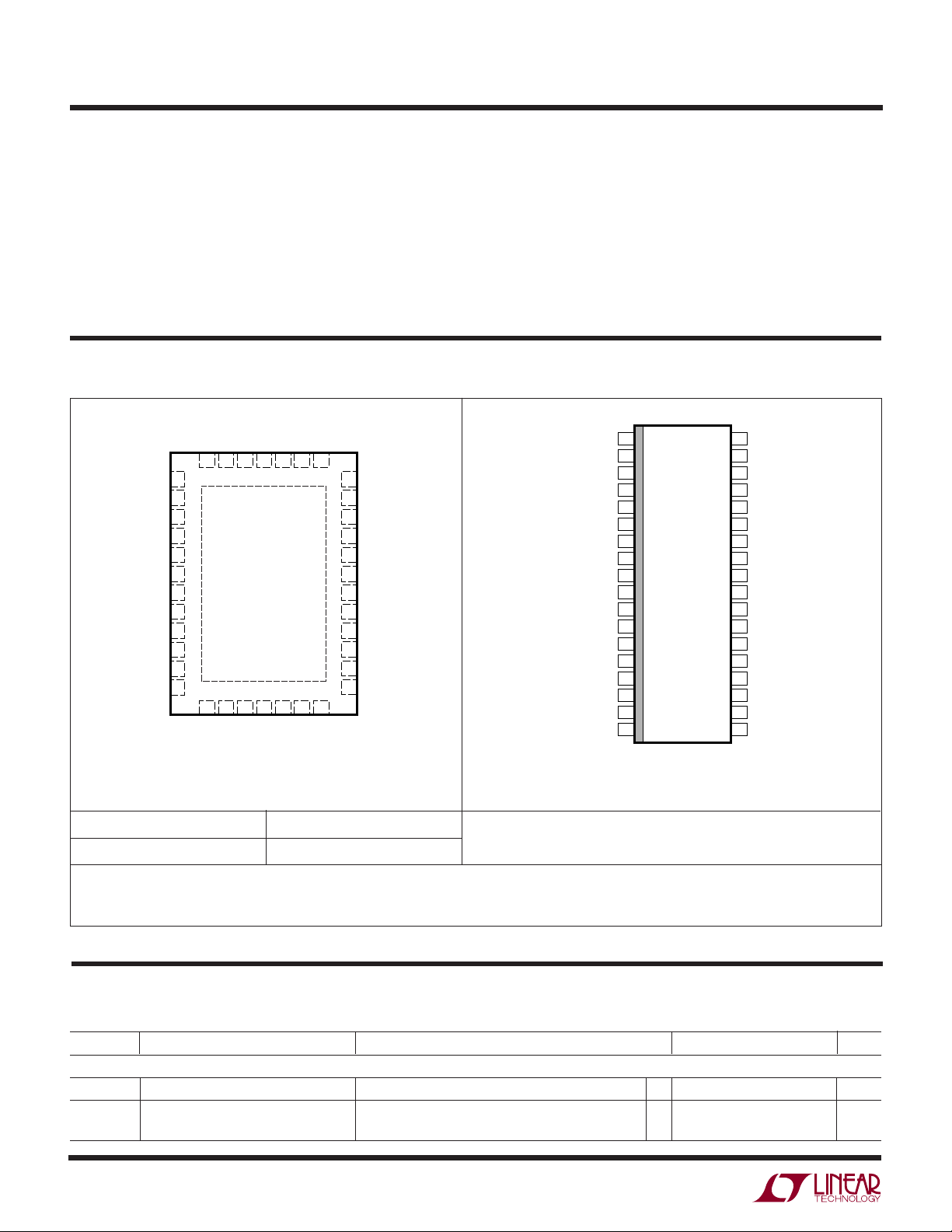
TOP VIEW
LOPWR
GB2I
GB2O
GB1I
GB1O
GDCI
GDCO
38 37 36 35 34 33 32
1V
SET
I
2
TH
I
3
SET
GND
4
DCDIV
5
SSB
6
SCK
7
MISO
8
MOSI
9
GND
10
CSN
11
CSP
12
13 14 15 16
CLP
38-LEAD (5mm × 7mm) PLASTIC QFN
T
THE EXPOSED PAD (PIN 39) IS GND. MUST BE SOLDERED TO THE PCB.
JMAX
39
17 18 19
CC
V
PGND
BGATE
COMP1
UHF PACKAGE
= 125°C, θJA = 34°C/W
UHF PART MARKING
LTC1960CUHF
Order Options Tape and Reel: Add #TR
Lead Free: Add #PBF Lead Free Tape and Reel: Add #TRPBF
Lead Free Part Marking: http://www.linear.com/leadfree/
Consult LTC Marketing for parts specified with wider operating temperature ranges.
DCIN
SW
31
SCP
SCN
30
BAT1
29
BAT2
28
V
27
GND
26
SCH2
25
GCH2
24
GCH1
23
22
SCH1
21
TGATE
20
BOOST
1960
PLUS
SSB, SCK, MOSI, MISO to GND................... 7V to –0.3V
COMP1 to GND ............................................ 5V to –0.3V
Operating Ambient Temperature
Range (Note 7) ........................................0°C to 70°C
Operating Junction Temperature .......... –40°C to 125°C
Storage Temperature ............................ –65°C to 185°C
Lead Temperature (Soldering, 10 sec).................. 300°C
TOP VIEW
V
PLUS
BAT2
BAT1
SCN
SCP
GDCO
GDCI
GB1O
GB1I
GB2O
GB2I
LOPWR
V
SET
I
I
SET
GND
DCDIV
SSB
1
2
3
4
5
6
7
8
9
10
11
12
13
14
TH
15
16
17
18
G PACKAGE
36-LEAD PLASTIC SSOP
T
= 125°C, θJA = 95°C/ W
JMAX
36
35
34
33
32
31
30
29
28
27
26
25
24
23
22
21
20
19
SCH2
GCH2
GCH1
SCH1
TGATE
BOOST
SW
DCIN
V
CC
BGATE
PGND
COMP1
CLP
CSP
CSN
MOSI
MISO
SCK
ORDER PART NUMBER
LTC1960CG
ELECTRICAL CHARACTERISTICS
temperature range (Note 7), otherwise specifications are at T
The ● denotes specifications which apply over the full operating
= 25°C.
V
A
DCIN
= 20V, V
BAT1
= 12V, V
= 12V unless otherwise noted.
BAT2
SYMBOL PARAMETER CONDITIONS MIN TYP MAX UNITS
Supply and Reference
DCIN Operating Range DCIN Selected 6 28 V
I
CH
DCIN Operating Current Not Charging (DCIN Selected) 1 1.5 mA
Charging (DCIN Selected) 1.3 2 mA
1960fa
2
Page 3
LTC1960
ELECTRICAL CHARACTERISTICS
temperature range (Note 7), otherwise specifications are at T
The ● denotes specifications which apply over the full operating
= 25°C.
V
A
DCIN
= 20V, V
BAT1
= 12V, V
= 12V unless otherwise noted.
BAT2
SYMBOL PARAMETER CONDITIONS MIN TYP MAX UNITS
Supply and Reference
Battery Operating Voltage Range Battery Selected, PowerPath Function (Note 2) 6 28 V
Battery Drain Current Battery Selected, Not Charging, V
V
Diodes Forward Voltage:
PLUS
V
V
V
V
FDC
FB1
FB2
FSCN
DCIN to V
BAT1 to V
BAT2 to V
SCN to V
PLUS
PLUS
PLUS
PLUS
UVLO Undervoltage Lockout Threshold V
UVHYS UV Lockout Hysteresis V
V
VCC
V
LDR
VCC Regulator Output Voltage 5 5.2 5.4 V
VCC Load Regulation I
I
= 10mA 0.8 V
VCC
I
= 0mA 0.7 V
VCC
I
= 0mA 0.7 V
VCC
I
= 0mA 0.7 V
VCC
Ramping Down, Measured at V
PLUS
Rising, Measured at V
PLUS
= 0mA to 10mA 0.2 1 %
VCC
= 0V 175 µA
DCIN
to GND
PLUS
to GND 60 mV
PLUS
●
3 3.5 3.9 V
Switching Regulator
V
I
f
f
TOL
TOL
0SC
DO
Overall Voltage Accuracy 5V ≤ V
Overall Current Accuracy IDAC Value = 3FF
V
< 25V, (Note 3) –0.8 0.8 %
CSP
, V
OUT
CSN
HEX
= 12V
●
–1 1 %
–5 5 %
●
–6 6 %
Regulator Switching Frequency 255 300 345 kHz
Regulator Switching Frequency in Low Duty Cycle ≥99% 20 25 kHz
Dropout Mode
DC
I
MAX
I
SNS
MAX
Regulator Maximum Duty Cycle 99 99.5 %
Maximum Current Sense Threshold V
CA1 Input Bias Current V
= 2.2V 140 155 190 mV
ITH
= V
CSP
> 5V 150 µA
CSN
CMSL CA1/I1 Input Common Mode Low 0 V
CMSH CA1/I1 Input Common Mode High V
V
CL1
CL1 Turn-On Threshold 95 100 105 mV
–0.2 V
DCIN
TGATE Transition Time:
TG t
TG t
r
f
TGATE Rise Time C
TGATE Fall Time C
= 3300pF, 10% to 90% 50 90 ns
LOAD
= 3300pF, 10% to 90% 50 90 ns
LOAD
BGATE Transition Time:
BG t
BG t
r
f
BGATE Rise Time C
BGATE Fall Time C
= 3300pF, 10% to 90% 50 90 ns
LOAD
= 3300pF, 10% to 90% 40 80 ns
LOAD
Trip Points
V
V
I
V
V
V
BVT
TR
THYS
TSC
FTO
OVSD
DCDIV/LOPWR Threshold V
DCDIV/LOPWR Hysteresis Voltage V
DCDIV/LOPWR Input Bias Current V
Short-Circuit Comparator Threshold V
Fast Power Path Turn-Off Threshold V
Overvoltage Shutdown Threshold as a V
or V
DCDIV
or V
DCDIV
or V
DCDIV
– V
SCP
SCN
Rising from V
DCDIV
Rising from 0.8V until TGATE and BGATE 107 %
SET
Falling
LOPWR
Rising 30 mV
LOPWR
= 1.19V 20 200 nA
LOPWR
, V
≥ 5V
CC
CC
●
1.166 1.19 1.215 V
●
90 100 115 mV
6 7 7.9 V
Percent of Programmed Charger Voltage Stop Switching
DACs
I
RES
IDAC Resolution Guaranteed Monotonic Above I
/16 10 bits
MAX
IDAC Pulse Period:
t
IP
t
ILOW
Normal Mode 61015 µs
Low Current Mode 50 ms
1960fa
3
Page 4
LTC1960
ELECTRICAL CHARACTERISTICS
temperature range (Note 7), otherwise specifications are at T
The ● denotes specifications which apply over the full operating
= 25°C.
V
A
DCIN
= 20V, V
BAT1
= 12V, V
= 12V unless otherwise noted.
BAT2
SYMBOL PARAMETER CONDITIONS MIN TYP MAX UNITS
DACs
V
V
V
t
RES
STEP
OFF
VP
VDAC Resolution Guaranteed Monotonic (5V < V
< 25V) 11 bits
BAT
VDAC Granularity 16 mV
VDAC Offset (Note 6) 0.8 V
VDAC Pulse Period 7 11 16.5 µs
Charge Mux Switches
t
ONC
t
OFFC
V
CON
V
COFF
V
TOC
V
FC
I
OC(SRC)
I
OC(SNK)
V
CHMIN
GCH1/GCH2 Tur-On Time V
GCH1/GCH2 Turn-Off Time V
CH Gate Clamp Voltage I
GCH1 V
GCH2 V
CH Gate Off Voltage I
GCH1 V
GCH2 V
CH Switch Reverse Turn-Off Voltage V
CH Switch Forward Regulation Voltage V
GCH1/GCH2 Active Regulation: V
GCHX
GCHX
V
CSN
LOAD
LOAD
CSN
BATX
GCHX
– V
– V
< V
BATX
= 1µA
GCH1
GCH2
=10µA
GCH1
GCH2
– V
BATX,
– V
– V
> 3V, V
SCHX
< 1V, from Time of 3 7 µs
SCHX
– 30mV, V
– V
SCH1
– V
SCH2
– V
SCH1
– V
SCH2
5V ≤ V
5V ≤ V
CSN,
= 1.5V
SCHX
SCHX
BATX
BATX
= TBD, C
= TBD, C
SCHX
≤ 28V
≤ 28V
= 3nF 5 10 ms
LOAD
= 3nF
LOAD
5 5.8 7 V
5 5.8 7 V
–0.8 –0.4 0 V
–0.8 –0.4 0 V
●
52040 mV
●
15 35 60 mV
Max Source Current –2 µA
Max Sink Current 2 µA
BATX Voltage Below Which 3.5 4.7 V
Charging is Inhibited (Does Not Apply
to Low Current Mode)
PowerPath Switches
t
DLY
t
PPB
t
ONPO
Blanking Period after UVLO Trip Switches Held Off 250 ms
Blanking Period after LOPWR Trip Switches in 3-Diode Mode 1 sec
GB1O/GB2O/GDCO Turn-On Time VGS < –3V, from Time of Battery/DC
●
510 µs
Removal, or LOPWR Indication
t
OFFPO
GB1O/GB2O/GDCO Turn-Off Time VGS > –1V, from Time of Battery/DC
●
37 µs
Removal, or LOPWR Indication
V
PONO
V
POFFO
V
TOP
V
FP
Output Gate Clamp Voltage I
LOAD
GB1O Highest (V
GB2O Highest (V
GDCO Highest (V
Output Gate Off Voltage I
LOAD
GB1O Highest (V
GB2O Highest (V
GDCO Highest (V
PowerPath Switch Reverse V
SCP
– V
Turn-Off Voltage 6V ≤ V
PowerPath Switch Forward V
BATX
Regulation Voltage 6V ≤ V
= 1µA
= –25µA
BATX
≤ 28V
SCP
– V
SCP
≤ 28V
SCP
BAT1
BAT2
DCIN
BAT1
BAT2
DCIN
or V
or V
or V
or V
or V
or V
or V
or V
SCP
DCIN
SCP
SCP
SCP
SCP
SCP
SCP
– V
– V
) – V
) – V
) – V
) – V
) – V
) – V
DCIN
SCP
GB1O
GB2O
GDCO
GB1O
GB2O
GDCO
4.75 6.25 7 V
4.75 6.25 7 V
4.75 6.25 7 V
0.18 0.25 V
0.18 0.25 V
0.18 0.25 V
●
52060 mV
●
02550 mV
GDCI/GB1I/GB2I Active Regulation (Note 4)
I
OP(SRC)
I
OP(SNK)
Source Current –4 µA
Sink Current 75 µA
4
1960fa
Page 5
LTC1960
ELECTRICAL CHARACTERISTICS
temperature range (Note 7), otherwise specifications are at T
The ● denotes specifications which apply over the full operating
= 25°C.
V
A
DCIN
= 20V, V
BAT1
= 12V, V
= 12V unless otherwise noted.
BAT2
SYMBOL PARAMETER CONDITIONS MIN TYP MAX UNITS
t
ONPI
t
OFFPI
V
PONI
V
POFFI
Gate B1I/B2I/DCI Turn-On Time VGS < –3V, C
Gate B1I/B2I/DCI Turn-Off Time VGS > –1V, C
Input Gate Clamp Voltage I
GB1I Highest (V
GB2I Highest (V
GDCI Highest (V
Input Gate Off Voltage I
GB1I Highest (V
GB2I Highest (V
GDCI Highest (V
LOAD
LOAD
= 1µA
BAT1
BAT2
DCIN
= –25µA
BAT1
BAT2
DCIN
= 3nF (Note 5) 300 µs
LOAD
= 3nF (Note 5) 10 µs
LOAD
or V
or V
or V
or V
or V
or V
SCP
SCP
SCP
SCP
SCP
SCP
) – V
) – V
) – V
) – V
) – V
) – V
GB1I
GB2I
GDCI
GB1I
GB2I
GDCI
4.75 6.7 7.5 V
4.75 6.7 7.5 V
4.75 6.7 7.5 V
0.18 0.25 V
0.18 0.25 V
0.18 0.25 V
Logic I/O
IIH/I
V
IL
V
IH
V
OL
I
OFF
IL
SSB/SCK/MOSI Input High/Low Current
SSB/MOSI/SCK Input Low Voltage
SSB/MOSI/SCK Input High Voltage
MISO Output Low Voltage IOL = 1.3mA
MISO Output Off-State Leakage Current V
MISO
= 5V
●
–1 1 µA
●
●
2V
●
●
0.8 V
0.4 V
2 µA
SPI Timing (See Timing Diagram)
T
WD
t
SSH
t
CYC
t
SH
t
SL
t
LD
t
LG
t
su
t
H
t
A
t
dis
t
V
t
HO
t
Ir
t
If
t
Of
Note 1: Stresses beyond those listed under Absolute Maximum Ratings
may cause permanent damage to the device. Exposure to any Absolute
Maximum Rating condition for extended periods may affect device
reliability and lifetime.
Note 2. Battery voltage must be adequate to drive gates of PowerPath
P-channel FET switches. This does not affect charging voltage of the
battery, which can be zero volts.
Note 3. See Test Circuit.
Note 4. DCIN, BAT1, BAT2 are held at 12V and GDCI, GB1I, GB2I are
Watch Dog Timer
●
1.2 2.5 4.5 sec
SSB High Time 680 ns
SCK Period C
LOAD
= 200pF R
= 4.7k on MISO
PULLUP
●
2 µs
SCK High Time 680 ns
SCK Low Time 680 ns
Enable Lead Time 200 ns
Enable Lag Time 200 ns
Input Data Set-Up Time
Input Data Hold Time
Access Time (From Hi-Z to Data Active on MISO)
Disable Time (Hold Time to Hi-Z State on MISO)
Output Data Valid CL = 200pF, R
Output Data Hold
= 4.7k on MISO
PULLUP
●
100 ns
●
100 ns
●
●
●
●
0ns
125 ns
125 ns
580 ns
SCK/MOSI/SSB Rise Time 0.8V to 2V 250 ns
SCK/MOSI/SSB Fall Time 2V to 0.8V 250 ns
MISO Fall Time 2V to 0.4V, CL = 200 pF
●
400 ns
GB1I and GB2I. SCP is set at 11.9V to measure sink current at GDCI, GB1I
and GB2I.
Note 5. Extrapolated from testing with C
= 50pF.
L
Note 6. VDAC offset is equal to the reference voltage, since
= V
V
OUT
(16mV • VDAC
REF
(VALUE)
/2047 + 1).
Note 7. The LTC1960C is guaranteed to meet specified performance from
0°C to 70°C and is designed, characterized and expected to meet specified
performance at –40°C and 85°C, but is not tested at these extended
temperature limits.
forced to 10.5V. SCP is set at 12.0V to measure source current at GDCI,
1960fa
5
Page 6
LTC1960
TIME (ms)
–4 –2
BAT1 VOLTAGE (V)
14
12
10
8
6
4
2
0
1960 G05
42
10 12 14 16
0
68
VIN = 20V
VDAC = 12.29V
IDAC = 3000mA
LOAD CURRENT = 1A
T
A
= 25°C
BAT1
OUTPUT
LOAD
CONNECTED
LOAD
DISCONNECTED
UW
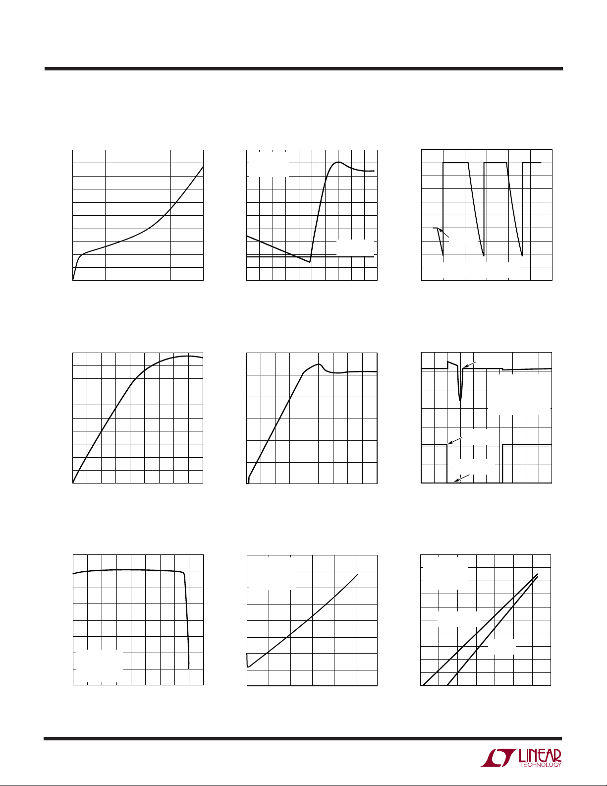
TYPICAL PERFOR A CE CHARACTERISTICS
Battery Drain Current
(BAT1 Selected)
250
TA = 25°C
240
230
220
210
200
190
180
BAT1 CURRENT (µA)
170
160
150
6
12
Charger Efficiency
100
90
80
70
60
50
40
EFFICIENCY (%)
30
20
10
0
0.025
0
18
BAT1 VOLTAGE (V)
0.50
0.10
I
(A)
OUT
Power Path Autonomous
Power Path Switching
16
C
= 20µF
LOAD
15
= 0.8A
I
LOAD
= 25°C
T
A
14
13
12
11
10
LOAD VOLTAGE (V)
9
8
7
24
30
1960 G01
6
–50 –40 –30
–20
–10
TIME (µs)
LOPWR
THRESHOLD
10 20 30 40 50
0
1960 G02
Charger Start-Up
12
10
8
6
4
CHARGER OUTPUT (V)
2
2.5 4.0
1960 G14
0
–0.05
0 0.10
0.05
0.30
0.20 0.40
0.25
0.15
TIME (SEC)
0.35
1960 G04
Switching
16
15
14
13
12
11
10
LOAD VOLTAGE (V)
9
8
7
6
BAT1
REMOVED
NOTE: LIGHT LOAD TO
EXAGGERATE SWITCHING EVENT
–1
0
1
Charger Load Dump
23
TIME (SEC)
4
5
1960 G03
6
Charger Load Regulation
12.4
12.3
12.2
12.1
12.0
11.9
BAT1 VOLTAGE (V)
11.8
11.7
11.6
VIN = 20V
VDAC = 12.288V
IDAC = 4000mA
= 25°C
T
A
1000 2000 3000
0
CHARGE CURRENT (mA)
4000
1960 G06
Charging Current Accuracy
120
V
= 20V
DCIN
= 12V
V
BAT1
100
OUTPUT CURRENT ERROR (mA)
–20
–40
80
60
40
20
0
0 200
R
SNS
= 25°C
T
A
= 0.025Ω
400 800600
IDAC VALUE
1000
1200
1960 G07
IDAC Low Current Mode vs
Normal Mode
500
VIN = 20V
450
400
350
300
250
200
150
CHARGING CURRENT (mA)
100
50
= 12V
V
BAT1
= 0.025Ω
R
SNS
= 25°C
T
A
LOW CURRENT
MODE
0
0
160
80
PROGRAMMED CURRENT (mA)
240
NORMAL
MODE
320
400
480
560
1960 G08
1960fa
Page 7
UW
BAT2
VOLTAGE
BAT2
CURRENT
BAT1
CURRENT
BAT1
VOLTAGE
BAT1 INITIAL CAPACITY = 0%
BAT2 INITIAL CAPACITY = 90%
PROGRAMMED CHARGER CURRENT = 3A
PROGRAMMED CHARGER VOLTAGE = 16.8V
TIME (MINUTES)
0
BATTERY VOLTAGE (V)
120
1960 G11
40 80 160
17.0
16.5
16.0
15.5
15.0
14.5
14.0
13.5
20 60 100 140
BATTERY CURRENT (mA)
3500
3000
2500
2000
1500
1000
500
0
TYPICAL PERFOR A CE CHARACTERISTICS
Voltage Accuracy
100
DCIN = 24V
= 25°C
T
A
75
50
25
–25
–50
OUTPUT VOLTAGE ERROR (mV)
–75
–100
I
LOAD
0
250 450
= 100mA
650 1050850
VDAC VALUE
1250
1450
1960 G09
Dual vs Sequential Charging
3500
3000
2500
2000
1500
1000
500
0
3500
3000
2500
2000
BATTERY CURRENT (mA)
1500
1000
500
0
0
BATTERY TYPE: 10.8V Li-Ion (MOLTECH NI2020)
REQUESTED CURRENT = 3A
REQUESTED VOLTAGE = 12.3V
MAX CHARGER CURRENT = 4.1A
BAT1
CURRENT
50
BAT1
CURRENT
100 150 200 250 300
TIME (MINUTES)
BAT2
CURRENT
BAT2
CURRENT
MINUTES
SEQUENTIAL
DUAL
100
LTC1960
Dual Charging Batteries with
Different Charge State
1960 G10
12.0
11.0
10.0
9.0
8.0
12.0
11.0
BATTERY VOLTAGE (V)
10.0
9.0
8.0
Dual vs Sequential Discharge
BAT1
VOLTAGE
BAT2
VOLTAGE
BAT2
VOLTAGE
BAT1
VOLTAGE
60 80 100 140
20 180
0
40
TIME (MINUTES)
BATTERY TYPE: 10.8V Li-Ion(MOLTECH NI2020)
LOAD CURRENT = 3A
DUAL
SEQUENTIAL
11
MINUTES
120
160
1960 G12
Dual vs Sequential Discharge
15
14
13
12
11
10
15
14
13
BATTERY VOLTAGE (V)
12
11
10
20
0
BATTERY TYPE: 12V NIMH (MOLTECH NJ1020)
LOAD: 33W
BAT2
VOLTAGE
BAT1
VOLTAGE
40
TIME (MINUTES)
BAT2
VOLTAGE
BAT1
VOLTAGE
60 80 100 140
DUAL
SEQUENTIAL
MINUTES
16
120
1960 G13
1960fa
7
Page 8

LTC1960
PIN FUNCTIONS
UUU
(G/UHF)
Input Power Related
SCN (Pin 4/Pin 30): PowerPath Current Sensing Negative
Input. This pin should be connected directly to the “bottom” (output side) of the low valued resistor in series with
the three PowerPath switch pairs, for detecting shortcircuit current events. Also powers LTC1960 internal
circuitry when all other sources are absent.
SCP (Pin 5/Pin 31): PowerPath Current Sensing Positive
Input. This pin should be connected directly to the “top”
(switch side) of the low valued resistor in series with the
three PowerPath switch pairs, for detecting short-circuit
current events.
GDCO (Pin 6/Pin 32): DCIN Output Switch Gate Drive.
Together with GDCI, this pin drives the gate of the Pchannel switch in series with the DCIN input switch.
GDCI (Pin 7/Pin 33): DCIN Input Switch Gate Drive.
Together with GDCO, this pin drives the gate of the Pchannel switch connected to the DCIN input.
GB1O (Pin 8/Pin 34): BAT1 Output Switch Gate Drive.
Together with GB1I, this pin drives the gate of the Pchannel switch in series with the BAT1 input switch.
GB1I (Pin 9/Pin 35): BAT1 Input Switch Gate Drive.
Together with GB1O, this pin drives the gate of the Pchannel switch connected to the BAT1 input.
GB2O (Pin 10/Pin 36): BAT2 Output Switch Gate Drive.
Together with GB2I, this pin drives the gate of the Pchannel switch in series with the BAT2 input switch.
GB2I (Pin 11/Pin 37): BAT2 Input Switch Gate Drive.
Together with GB2O, this pin drives the gate of the Pchannel switch connected to the BAT2 input.
CLP (Pin 24/Pin 13): This is the Positive Input to the
Supply Current Limiting Amplifier CL1. The threshold is
set at 100mV above the voltage at the DCIN pin. When
used to limit supply current, a filter is needed to filter out
the switching noise.
Battery Charging Related
V
(Pin 13/Pin 1): The Tap Point of a Programmable
SET
Resistor Divider which Provides Battery Voltage Feedback
to the Charger. A capacitor from CSN to V
V
to GND provide necessary compensation and filter-
SET
ing for the voltage loop.
(Pin 14/Pin 2): This is the Control Signal of the Inner
I
TH
Loop of the Current Mode PWM. Higher I
to higher charging current in normal operation. A capacitor of at least 0.1µF to GND filters out PWM ripple. Typical
full-scale output current is 30µA. Nominal voltage range
for this pin is 0V to 2.4V.
I
(Pin 15/Pin 3): A Capacitor from I
SET
Required to Filter Higher Frequency Components from the
Delta-Sigma IDAC.
CSN (Pin 22/Pin 11): Current Amplifier CA1 Input. Connect this to the common output of the charger MUX
switches.
CSP (Pin 23/Pin 12): Current Amplifier CA1 Input. This
pin and the CSN pin measure the voltage across the sense
resistor, RSNS, to provide the instantaneous current
signals required for both peak and average current mode
operation.
COMP1 (Pin 25/Pin 14): This is the Compensation Node
for the Amplifier CL1. A capacitor is required from this pin
to GND if input current amplifier CL1 is used. At input
adapter current limit, this node rises to 1V. By forcing
COMP1 low, amplifier CL1 will be defeated (no adapter
current limit). COMP1 can source 10µA.
BGATE (Pin 27/Pin 16): Drives the Bottom External MOSFET
of the Battery Charger Buck Converter.
SW (Pin 30/Pin 19): Connected to Source of Top External
MOSFET Switch. Used as reference for top gate driver.
BOOST (Pin 31/Pin 20): Supply to Topside Floating Driver.
The bootstrap capacitor is returned to this pin. Voltage
swing at this pin is from a diode drop below VCC to (DCIN
+ VCC).
and one from
SET
corresponds
TH
to Ground is
SET
8
1960fa
Page 9

UUU
PIN FUNCTIONS
LTC1960
(G/UHF)
TGATE (Pin 32/Pin 21): Drives the Top External MOSFET
of the Battery Charger Buck Converter.
SCH1 (Pin 33/Pin 22), SCH2 (Pin 36/Pin 25): Charger
MUX Switch Source Returns. These two pins are connected to the sources of Q3/Q4 and Q9/Q10 (see Typical
Application on back page of data sheet), respectively. A
small pull-down current source returns these nodes to 0V
when the switches are turned off.
GCH1 (Pin 34/Pin 23), GCH2 (Pin 35/Pin 24): Charger
MUX Switch Gate Drives. These two pins drive the gates of
the back-to-back N-channel switch pairs, Q3/Q4 and Q9/
Q10, between the charger output and the two batteries.
External Power Supply Pins
V
(Pin 1/Pin 27): Supply. The V
PLUS
via four internal diodes to the DCIN, SCN, BAT1, and
BAT2 pins. Bypass this pin with a 1µF to 2µF capacitor.
BAT1 (Pin 3/Pin 29), BAT2 (Pin 2/Pin 28): These two
pins are the inputs from the two batteries for power to the
LTC1960 and to provide voltage feedback to the battery
charger.
LOPWR (Pin 12/Pin 38): LOPWR Comparator Input from
External Resistor Divider Connected from SCN to GND. If
the voltage at LOPWR is lower than the LOPWR comparator threshold, then system power has failed and
power is autonomously switched to a higher voltage
source, if available. See PowerPath section of LTC1960
operation.
DCDIV (Pin 17/Pin 5): DCDIV Comparator Input from
External Resistor Divider Connected from DCIN to
GND. If the voltage at DCDIV is above the DCDIV
comparator threshold, then the DC bit is set and the
wall adapter power is considered to be adequate to
charge the batteries. If DCDIV is taken more than 1.8V
pin is connected
PLUS
above V
off until all power is removed.
DCIN (Pin 29/Pin 18): Supply. External DC power source.
A 1µF bypass capacitor should be connected to this pin
as close as possible. No series resistance is allowed,
since the adapter current limit comparator input is also
this pin.
, then all of the power path switches are latched
CC
Internal Power Supply Pins
GND (Pin 16/Pin 4, Pin 10, Pin 26, Pin 39): Ground for
Low Power Circuitry.
PGND (Pin 26/Pin 15): High Current Ground Return for
BGATE Driver.
V
(Pin 28/Pin 17): Internal Regulator Output. Bypass
CC
this output with at least a 2µF to 4.7µF capacitor. Do not
use this regulator output to supply more than 1mA to
external circuitry.
Digital Interface Pins
SSB (Pin 18/Pin 6): SPI Slave Select Input. Active low.
TTL levels. This signal is low when clocking data to/from
the LTC1960.
SCK (Pin 19/Pin 7): Serial SPI Clock. TTL levels.
MISO (Pin 20/Pin 8): SPI Master-In-Slave-Out Output,
Open Drain. Serial data is transmitted from the LTC1960,
when SSB is low, on the falling edge of SCK. TTL levels.
A 4.7k pullup resistor is recommended.
MOSI (Pin 21/Pin 9): SPI Master-Out-Slave-In Input.
Serial data is transmitted to the LTC1960, when SSB is
low, on the rising edge of SCK. TTL levels.
Exposed Pad (Pin 39, UHF Package Only): Ground.
Must be soldered to the PCB ground for rated thermal
performance.
1960fa
9
Page 10

LTC1960
BLOCK DIAGRA
PLUS
V
GND
V
SW
CLP
CHARGE
PUMP
ON
34
33
ON
35
36
3
2
1
28
CC
SET
16
29
13
31
32
30
27
26
24
V
REGULATOR
OSCILLATOR
LOW DROP
DETECT
100mV
DCIN
GCH1
SCH1
GCH2
SCH2
BAT1
BAT2
V
DCIN
BGATE
BOOST
TGATE
BGATE
PGND
DCIN
W
(LTC1960CG Pin Numbers Shown)
GB1I GB1O GB2I GB2O GDCI GDCO
9 8 11 10
SWB1
–
+
–
+
CC
T
ON
V
CC
+
CL1
–
25 14
COMP1
SCN
gm = 0.4m
CSN
CHGMON
PWM
LOGIC
Ω
400k
0.86V
0.8V
DRIVER
+
Q
CHARGE
I
DRIVER
CHARGE
–
0V
+
= 1.4m
g
–
m
EA
S
R
TH
SWB2
Ω
76
SWDC
DRIVER
11-BIT ∆Σ
VOLTAGE DAC
SHORT CIRCUIT
AC_PRESENT
SELECTOR
CONTROLLER
SPI
INTERFACE
11
gm = 1.4m
CURRENT DAC
CA1
÷15
I
CMP
I
REV
10-BIT ∆Σ
–
+
Ω
CA2
BUFFERED I
+
–
–
+
CLAMP
100mV
+
–
+
–
+
–
1.19V
3k
3k
–
+
0.8V
TH
+
–
40mV
–
0.75V
+
100Ω
5
4
17
12
21
20
19
18
15
CSP-CSN
3kΩ
23
22
CHGMON
1960 BD
SCP
SCN
DCDIV
LOPWR
MOSI
MISO
SCK
SSB
I
SET
CSP
CSN
U
W U
TEST CIRCUIT A D TI I G DIAGRA
Test Circuit
SSB
SCK
MOSI
MISO
BAT1
BAT2
CHGMON
+
V
REF
EA
–
V
SET
V
SW
I
TH
+
0.5V
–
1960 TC01
10
W
t
A
SPI Timing Diagram
t
SSH
t
LG
t
dis
1960 TD01
1960fa
t
H
SLAVE
BIT 7 OUT
t
CYC
t
SH
t
SL
BIT 0BIT 7
t
V
t
HO
SLAVE
BIT 0 OUT
t
LD
t
su
Page 11

OPERATIO
LTC1960
U
(Refer to Block Diagram and Typical Application)
OVERVIEW
The LTC1960 is composed of a battery charger controller,
charge MUX controller, PowerPath controller, SPI interface, a 10-bit current DAC (IDAC) and 11-bit voltage DAC
(VDAC). When coupled with a low cost microprocessor, it
forms a complete battery charger/selector system for two
batteries. The battery charger is programmed for voltage
and current, and the charging battery is selected via the
SPI interface. Charging can be accomplished only if the
voltage at DCDIV indicates that sufficient voltage is available from the input power source, usually an AC adapter.
The charge MUX, which selects the battery to be charged,
is capable of charging both batteries simultaneously by
selecting both batteries for charging. The charge MUX
switch drivers are configured to allow charger current to
share between the two batteries and to prevent current
from flowing in a reverse direction in the switch. The
amount of current that each battery receives will depend
upon the relative capacity of each battery and the battery
voltage. This can result in significantly shorter charging
times (up to 50% for Li-Ion batteries) than sequential
charging of each battery. In order to continue charging,
the CHARGE_BAT information must be updated more
frequently than the internal watchdog timer.
The PowerPath controller selects which of the pairs of
PFET switches, input and output, will provide power to the
system load. The selection is accomplished over the SPI
interface. If the system voltage drops below the threshold
set by the LOPWR resistor divider, then all of the output
side PFETs are turned on quickly and power is taken from
the highest voltage source available at the DCIN, BAT1 or
BAT2 inputs. The input side PFETs act as diodes in this
mode and power is taken from the source with the highest
voltage. The input side PowerPath switch driver that is
delivering power then closes its input switch to reduce the
power dissipation in the PFET bulk diode. In effect, this
system provides diode -like behavior from the FET switches,
without the attendant high power dissipation from diodes.
The microprocessor is informed of this 3-diode mode
status when it polls the PowerPath status register via the
SPI interface. The microprocessor can then assess which
power source is capable of providing power, and program
the PowerPath switches accordingly. Since high speed
PowerPath switching at LOPWR trip points is handled
autonomously, there is no need for real-time microprocessor resources to accomplish this task.
Simultaneous discharge of both batteries is accomplished
by simply programming both batteries for discharge into
the system load. The switch drivers prevent reverse current flow in the switches and automatically discharge both
batteries into the load, sharing current according to the
relative capacity of the batteries. Simultaneous dual discharge can increase battery operating time by approximately 10% by reducing losses in the switches and reducing
internal losses associated with high discharge rates.
SPI Interface
The SPI interface is used to write to the internal PowerPath
registers, the charger control registers, the current DAC,
and the voltage DAC. The SPI is also able to read internal
status registers. There are two types of SPI write commands. The first write command is a 1-byte command
used to load PowerPath and charger control bits. The
second write command is a 2-byte command used to load
the DACs. The SPI read command is a 2-byte command. In
order to ensure the integrity of the SPI communication, the
last bit received by the SPI is echoed back over the MISO
output after the next falling SCK. The data format is set up
so that the master has the option of aborting a write if the
returned MISO bit is not as expected.
1-Byte SPI Write Format:
bit 7........byte 1..........bit 0
MOSI D0 D1 D2 X A0 A1 A2 0
MISO X D0 D1 D2 X A0 A1 A2
Charger Write Address: A[2:0] = b111
Charger Write Data: D2 = X
D1 = CHARGE_BAT2
D0 = CHARGE_BAT1
PowerPath Write Address: A[2:0] = b110
PowerPath Write Data: D2 = POWER_BY_DC
D1 = POWER_BY_BAT2
D0 = POWER_BY_BAT1
1960fa
11
Page 12

LTC1960
U
OPERATIO
2-Byte SPI Write Format:
bit 7........byte 1..........bit 0 bit 7..........byte 2............bit 0
MOSI D0 D1 D2 D3 D4 D5 D6 1 D7 D8 D9 D10 A0 A1 A2 0
MISO X D0 D1 D2 D3 D4 D5 D6 1 D7 D8 D9 D10 A0 A1 A2
IDAC Write Address: A[2:0] = b000
IDAC Data Bits D9-D0: IDAC value data (MSB-LSB)
IDAC Data Bit D10 : Normal mode = 0, low current mode = 1 (Dual battery charging is disabled)
VDAC Write Address: A[2:0] = b001
VDAC Data Bits D10-D0: VDAC value (MSB-LSB)
Subsequent SPI communication is inhibited until after the addressed DAC is finished loading. It is recommended that
the master transmit all zeros until MISO goes low. This handshaking procedure is illustrated in Figure 1.
SSB
SCK
MOSI
MISO
BYTE 1
BYTE 2
Figure 1. SPI Write to VDAC of Data = b101_0101_0101
2-Byte SPI Read Format:
bit 7........byte 1.......bit 0 bit 7........byte 2............bit 0
MOSI 0 0 0 0 A0 A1 A2 0 0 0 0 0 A0 A1 A2 1
MISO X 0 0 0 0 A0 A1 A2 X FA LP DC PF CH X X
Status Address: A[2:0] = b010
Status Read Data: LP = LOW_POWER (Low power comparator output)
DC = DCDIV (DCDIV comparator output)
PF = POWER_FAIL (Set if selected power supply failed to hold up system power
after three tries)
1960 F01
CH = CHARGING (One or more batteries are being charged)
FA = FAULT. This bit is set for any of the following conditions:
1) The LTC1960 is still in power on reset.
2) The LTC1960 has detected a short circuit and has shut down power and charging.
3) The system has asserted a fast off using DCDIV.
Note: All other values of A[2:0] are reserved and must not be used.
12
1960fa
Page 13

U
OPERATIO
A status read is illustrated in Figure 2.
LTC1960
SSB
SCK
MOSI
MISO
Figure 2. SPI Read of FA = 0, LP = 0, DC = 1, PF = 0, and CH = 1
BYTE 1 BYTE 2
Battery Charger Controller
The LTC1960 charger controller uses a constant off-time,
current mode step-down architecture. During normal operation, the top MOSFET is turned on each cycle when the
oscillator sets the SR latch and turned off when the main
current comparator I
resets the SR latch. While the top
CMP
MOSFET is off, the bottom MOSFET is turned on until
either the inductor current reverses, as indicated by current comparator IREV, or the beginning of the next cycle.
The oscillator uses the equation:
t
OFF
= 1/f
OSC
• (V
DCIN
– V
CSN
)/V
DCIN
to set the bottom MOSFET on time. The peak inductor
current at which ICMP resets the SR latch is controlled by
the voltage on I
. ITH is in turn controlled by several loops,
TH
depending upon the situation at hand. The average current
control loop converts the voltage between CSP and CSN to
a representative current. Error amp CA2 compares this
current against the desired current requested by the IDAC
at the I
pin and adjusts ITH until the IDAC value is
SET
satisfied. The BAT1/BAT2 MUX provides the selected
battery voltage at CHGMON, which is divided down to the
pin by the VDAC resistor divider and is used by error
V
SET
amp EA to decrease I
if the V
TH
voltage is above the 0.8V
SET
reference. The amplifier CL1 monitors and limits the input
current, normally from the AC adapter, to a preset level
(100mV/RCL). At input current limit, CL1 will decrease the
I
voltage and thus reduce battery charging current.
TH
An overvoltage comparator, 0V, guards against transient
overshoots (>7%). In this case, the top MOSFET is turned
off until the overvoltage condition is cleared. This feature
is useful for batteries which “load dump”
themselves by opening their protection switch to perform
functions such as calibration or pulse mode charging.
1960 F05
Charging is inhibited for battery voltages below the minimum charging threshold, V
. Charging is not inhib-
CHMIN
ited when the low current mode of the IDAC is selected.
The top MOSFET driver is powered from a floating bootstrap capacitor C
from V
through an external diode when the top MOSFET
CC
is turned off. A 2µF to 4.7µF capacitor across V
. This capacitor is normally recharged
B
to GND
CC
is required to provide a low dynamic impedance to charge
the boost capacitor. It is also required for stability and
power-on-reset purposes.
decreases towards the selected battery voltage, the
As V
IN
converter will attempt to turn on the top MOSFET continuously (“dropout’’). A dropout timer detects this condition
and forces the top MOSFET to turn off, and the bottom
MOSFET on, for about 200ns at 40µs intervals to recharge
the bootstrap capacitor.
Charge MUX Switches
The equivalent circuit of a charge MUX switch driver is
shown in Figure 3. If the charger controller is not enabled,
the charge MUX drivers will drive the gate and source of
the series connected MOSFETs to a low voltage and the
switch is off. When the charger controller is on, the charge
MUX driver will keep the MOSFETs off until the voltage at
CSN rises at least 35mV above the battery voltage. GCH1
is then driven with an error amplifier EAC until the voltage
between BAT1 and CSN satisfies the error amplifier or until
GCH1 is clamped by the internal Zener diode. The time
required to close the switch could be quite long (many ms)
due to the small currents output by the error amp and
depending upon the size of the MOSFET switch.
If the voltage at CSN decreases below V
– 20mV a
BAT1
comparator CC quickly turns off the MOSFETs to prevent
1960fa
13
Page 14

LTC1960
–
+
+
–
GB1I
GB1O
Q8
Q7
FROM
BATTERY
1
BAT1
SCP
25mV
20mV
OFF
OFF
1960 F04
EAP
CP
SWP
TO
LOAD
C
L
R
SC
OPERATIO
U
reverse current from flowing in the switches. In essence,
this system performs as a low forward voltage diode.
Operation is identical for BAT2.
DCIN + 10V
(CHARGE PUMPED)
BAT1
TO
BATTERY
FROM
CHARGER
1
CSN
35mV
20mV
–
EAC
+
+
CC
–
OFF
10k
GCH1
SCH1
Q3
Q4
1960 F03
Figure 3. Charge MUX Switch Driver Equivalent Circuit
Dual Charging
Note that the charge MUX switch drivers will operate
together to allow both batteries to be charged simultaneously. If both charge MUX switch drivers are enabled,
only the battery with the lowest voltage will be charged
until its voltage rises to equal the higher voltage battery.
The charge current will then share between the batteries
according to the capacity of each battery.
If both batteries are selected for charging, only batteries
with voltages above V
are allowed to charge. Dual
CHMIN
charging is not allowed when the low current mode of the
IDAC is selected. If dual charging is enabled when the IDAC
enters low current mode, then only BAT1 will be charged.
are usually connected as an input switch and an output
switch. The output switch PFET is connected in series with
the input PFET and the positive side of the short-circuit
sensing resistor, R
. The input switch is connected in
SC
series between the power source and the output PFET. The
PowerPath switch driver equivalent circuit is shown in
Figure 4. The output PFET is driven high and low by the
output side driver controlling pin GXXO, the PFET is either
on or off. The gate of the input PFET is driven by an error
amplifier which monitors the voltage between the input
power source (BAT1 in this case) and SCP. If the switch is
turned off, the two outputs are driven to the higher of the
two voltages present across the input/output terminals of
the switch. When the switch is instructed to turn on, the
output side driver immediately drives the gate of the
output PFET approximately 6V below the highest of the
voltages present at the input/output. When the output
PFET turns on, the voltage at SCP will be pulled up to a
diode drop below the source voltage by the bulk diode of
the input PFET. If the source voltage is more than 25mV
above SCP, EAP will drive the gate of the input PFET low
until the input PFET turns on and reduces the voltage
across the input/output to the EAP set point, or until the
Zener clamp engages to limit the voltage applied to the
input PFET. If the source voltage drops more than 20mV
below SCP, then comparator CP turns on SWP to quickly
prevent large reverse current in the switch. This operation
mimics a diode with a low forward voltage drop.
Charger Start-Up
When the charger controller is enabled by the SPI Interface block, the charger output CSN will ramp from 0V until
it exceeds the selected battery voltage. The clamp error
amp is used to prevent the charger output from exceeding
the selected battery voltage by more than 0.7V during the
start-up transient while the charge MUX switches, have
yet to close. Once the charge MUX switches have closed,
the clamp releases I
PowerPath Controller
The PowerPath switches are turned on and off via the SPI
interface, in any combination. The external P-MOSFETs
14
to allow control by another loop.
TH
Figure 4. PowerPath Driver Equivalent Circuit
1960fa
Page 15

OPERATIO
LTC1960
U
Autonomous PowerPath Switching
The LOPWR comparator monitors the voltage at the load
through the resistor divider from pin SCN. If any
POWER_BY bit is set and the LOPWR comparator trips,
then all of the switches are turned on (3-Diode mode) by
the PowerPath controller to ensure that the system is
powered from the source with the highest voltage. The
PowerPath controller waits approximately 1sec, to allow
power to stabilize, and then reverts to the previous
PowerPath switch configuration. A power fail counter is
incremented to indicate that a failure has occurred. If the
power fail counter equals a value of 3, then the PowerPath
controller sets the switches to 3-Diode mode and the PF bit
is set in the status register. This is a three-strikes-andyou’re-out process which is intended to debounce the
PowerPath PF indicator. The power fail counter is reset by
a power path SPI write.
Short-Circuit Protection
Short -circuit protection operates in both a current mode
and a voltage mode. If the voltage between SCP and SCN
exceeds the short-circuit comparator threshold V
TSC
for
more than 15ms, then all of the PowerPath switches are
turned off and the FAULT bit (FA) is set. Similarly, if the
voltage at SCN falls below 3V for more than 15ms, then all
of the PowerPath switches are turned off and the FA bit is
set. The FA bit is reset by removing all power sources and
allowing the voltage at V
to fall below the UVLO
PLUS
threshold. If the FA bit is set, charging is disabled until
V
exceeds the UVLO threshold and charging is
PLUS
requested via the SPI interface.
Fast PowerPath Turn-Off
All of the PowerPath switches can be forced off by setting
the DCDIV pin to a voltage between 8V and 10V. This will
have the same effect as a short-circuit event. The PF status
bit will also be set. DCDIV must be less than 5V and V
PLUS
must decrease below the UVLO threshold to re-enable the
PowerPath switches.
Power-Up Strategy
All three PowerPath switches are turned on after V
PLUS
exceeds the UVLO threshold for more than 250ms. This
delay is to prevent oscillation from a turn-on transient near
the UVLO threshold.
The Voltage DAC Block
The voltage DAC (VDAC) is a delta-sigma modulator which
controls the effective value of an internal resistor,
R
= 7.2k, used to program the maximum charger
VSET
voltage. Figure 5 is a simplified diagram of the VDAC
operation. The Charger Monitor MUX is connected to the
appropriate battery indicated by the CHARGE_BATx bit.
The delta-sigma modulator and switch SWV convert the
VDAC value, received via SPI communication, to a variable
resistance equal to (11/8)R
regulation, V
voltage, V
is servo driven to the 0.8V reference
SET
.
REF
VSET
/(VDAC
(VALUE)
/2047). In
Therefore programmed voltage is:
V
= (8/11) V
BATx
= 32,752mV • (VDAC
+ V
REF
405.3k/7.2k • (VDAC
REF
(VALUE)
(VALUE)
/2047)
/2047) + 0.8V
When a hard short-circuit occurs, it might pull all of the
power sources down to near 0V potentials. The capacitors
on V
and V
CC
must be large enough to keep the circuit
PLUS
operating correctly during the 15ms short-circuit event.
The charger will stop within a few microseconds leaving a
small current which must be provided by the capacitor on
V
. The recommended minimum values (1µF on V
PLUS
PLUS
and 2µF on VCC, including tolerances) should keep the
LTC1960 operating above the UVLO trip voltage long
enough to perform the short-circuit function when the
input voltages are greater than 8V. Increasing the capacitor across V
to 4.7µF will allow operation down to the
CC
recommended 6V minimum.
CSN
SWV
CHGMON
R
405.3k
V
R
VSET
7.2k
VF
REF
–
EA
+
∆Σ
MODULATOR
TO
I
TH
DAC
11
VALUE
(11 BITS)
1960 F05
1960fa
BAT1
BAT2
C
B2
V
SET
C
B1
Figure 5. Voltage DAC Operation
15
Page 16

LTC1960
OPERATIO
U
Note that the reference voltage must be subtracted from
the VDAC value in order to obtain the correct output
voltage. This value is V
Capacitors C
present at the V
and CB2 are used to average the voltage
B1
pin as well as provide a zero in the
SET
/16mV = 50 (32
REF
HEX
).
voltage loop to help stability and transient response time
to voltage variations. See Applications Information
section.
The Current DAC Block
The current DAC is a delta-sigma modulator which
controls the effective value of an internal resistor,
R
= 18.77k, used to program the maximum charger
SET
current. Figure 6 is a simplified diagram of the DAC
operation. The delta-sigma modulator and switch convert
the IDAC value, received via SPI communication, to a
variable resistance equal to 1.25R
In regulation, I
voltage, V
REF
is servo driven to the 0.8V reference
SET
, and the current from R
SET
/(IDAC
SET
(VALUE)
/1023).
is matched
against a current derived from the voltage between pins
CSP and CSN. This current is (V
CSP
– V
CSN
)/3k.
Therefore programmed current is:
= 0.8 V
I
AVG
= (102.3mV/R
REF
3k/(R
) • (IDAC
SNS
SNS RSET
(VALUE)
) • (IDAC
/1023)
(VALUE)
/1023)
When the low current mode bit (D10) is set to 1, the
current DAC enters a different mode of operation. The
current DAC output is pulse-width modulated with a high
frequency clock having a duty cycle value of 1/8. Therefore, the maximum output current provided by the charger
/8. The delta-sigma output gates this low duty cycle
is I
MAX
signal on and off. The delta-sigma shift registers are then
clocked at a slower rate, about 40ms/bit, so that the
charger has time to settle to the I
/8 value. The resulting
MAX
average charging current is equal to 1/8 of the current
programmed in normal mode. Dual battery charging is
disabled in low current mode. If both batteries are selected
for charging, then only BAT1 will charge.
(V
– V
CSP
(FROM CA1 AMPLIFIER)
I
SET
C
SET
R
18.77k
Figure 6. Current DAC Operation
I
/8
MAX
0
~ 40ms
Figure 7. Charging Current Waveform in Low Current Mode
)
CSN
3kΩ
V
REF
SET
MODULATOR
AVERAGE CHARGER CURRENT
+
–
∆Σ
TO
I
TH
DAC
10
VALUE
(10 BITS)
1960 F06
1960 F07
16
1960fa
Page 17

LTC1960
100mV
–
+
5kΩ
CLP
DCIN
11960 F08
0.1µF
+
RCL*
C
IN
V
IN
CL1
AC ADAPTER
INPUT
*R
CL
=
100mV
ADAPTER CURRENT LIMIT
+
U
WUU
APPLICATIONS INFORMATION
Automatic Current Sharing
In a dual parallel charge configuration, the LTC1960 does
not actually control the current flowing into each individual
battery. The capacity, or Amp-Hour rating, of each battery
determines how the charger current is shared. This automatic steering of current is what allows both batteries to
reach their full capacity points at the same time. In other
words, given all other things equal, charge termination will
happen simultaneously.
A battery can be modeled as a huge capacitor and hence
governed by the same laws.
I = C • (dV/dT) where:
I = The current flowing through the capacitor
C = Capacity rating of battery (using amp-hour values
instead of capacitance)
dV = Change in voltage
dt = Change in time
The equivalent model of a set or parallel batteries is a set
of parallel capacitors. Since they are in parallel, the change
in voltage over change in time is the same for both
batteries one and two.
dV/dt
From here we can simplify.
I
BAT1/CBAT1
I
BAT2
At this point you can see that the current divides as the
ratio of the two batteries capacity ratings. The sum of the
current into both batteries is the same as the current being
supply by the charger. This is independent of the mode of
the charger (CC or CV).
= dV/dt
BAT1
= dV/dt = I
= I
BAT1 CBAT2/CBAT1
BAT2
BAT2/CBAT2
is actual physical capacity rating at the time of charge.
Capacity rating will change with age and use and hence the
current sharing ratios can change over time.
In dual charge mode, the charger uses feedback from the
BAT2 input to determine charger output voltage. When
charging batteries with significantly different initial states
of charge (i.e. one almost full, the other almost depleted),
the full battery will get a much lower current. This will
cause a voltage difference across the charge MUX switches,
which may cause the BAT1 voltage to exceed the programmed voltage. Using MOSFETs in the charge MUX
with lower R
will alleviate this problem.
DS(0N)
Adapter Limiting
An important feature of the LTC1960 is the ability to
automatically adjust charging current to a level which
avoids overloading the wall adapter. This allows the product to operate at the same time that batteries are being
charged without complex load management algorithms.
Additionally, batteries will automatically be charged at the
maximum possible rate of which the adapter is capable.
This feature is created by sensing total adapter output
current and adjusting charging current downward if a
preset adapter current limit is exceeded. True analog
control is used, with closed loop feedback ensuring that
adapter load current remains within limits. Amplifier CL1
in Figure 8 senses the voltage across R
, connected
CL
between the CLP and DCIN pins. When this voltage exceeds 100mV, the amplifier will override programmed
charging current to limit adapter current to 100mV/R
CL
. A
lowpass filter formed by 5kΩ and 0.1µF is required to
eliminate switching noise. If the current limit is not used,
CLP should be connected to DCIN.
From here we solve for the actual current for each battery.
Please note that the actual observed current sharing will
vary from manufactures claimed capacity ratings since it
I
CHRG
I
BAT2
I
BAT1
= I
= I
= I
+ I
BAT1
CHRG CBAT2
CHRG CBAT1
BAT2
/(C
/(C
BAT1
BAT1
+ C
+ C
)
BAT2
)
BAT2
Figure 8. Adapter Current Limiting
1960fa
17
Page 18

LTC1960
U
WUU
APPLICATIONS INFORMATION
Watchdog Timer
Charging will begin when either CHARGE_BAT1 or
CHARGE_BAT2 bits are set in the charger register
(address: 111). Charging will stop if the charger register is
not updated prior to the expiration of the watchdog timer.
Simply repeating the same data transmission to the charger
register at a rate higher than once per second will ensure
that charging will continue uninterrupted.
Extending System to More than 2 Batteries
The LTC1960 can be extended to manage systems with
more than 3 sources of power. Contact Linear Technology
Applications Engineering for more information.
Charging Depleted Batteries
Some batteries contain internal protection switches that
disconnect a load if the battery voltage falls below what is
considered a reasonable minimum. In this case, the charger
may not start because the voltage at the battery terminal
is less than 5V. The low current mode of the IDAC must be
used in this case to condition the battery. In low current
mode, there is no minimum voltage requirement (but dual
charging is not allowed). Usually, the battery will detect
that it is being charged and then close its protection
switch, which will allow the IDAC to switch to normal
mode. Smart batteries require that charging current not
exceed 100mA until valid charging voltage and charging
current parameters are transmitted via the SMBus. The
low current IDAC mode is ideal for this purpose.
Starting Charge with Dissimilar Batteries
in Dual Charge Mode
When charging batteries of different charger termination
voltages, the charger should be started using the following
procedure:
Step 1. Select only the lowest termination voltage battery
for charging, and set the charger to its charging parameters.
Step 2. When the battery current is flowing into that
battery, change to dual charging mode (without stopping
the charger) and set the appropriate charging parameters
for this dual charger condition.
If this procedure is not followed, and BAT2 is significantly
higher voltage than BAT1, the charger could refuse to
charge either battery.
Charge Termination Issues
Batteries with constant-current charging and voltagebased charger termination might experience problems
with reductions of charger current caused by adapter
limiting. It is recommended that input limiting feature be
defeated in such cases. Consult the battery manufacturer
for information on how your battery terminates charging.
Setting Output Current Limit
The full scale output current setting of the IDAC will
produce V
the full scale current of the DAC simply divide V
R
.
SNS
= 102.3mV between CSP and CSN. To set
MAX
MAX
by
This is expressed by the following equation:
= 0.1023/I
R
SNS
Table 1. Recommended R
I
(A) R
MAX
1.023 0.100 0.25
2.046 0.050 0.25
4.092 0.025 0.5
8.184 0.012 1
MAX
Resistor Values
SNS
SNS
(Ω) 1% R
SNS
(W)
Use resistors with low ESL.
Inductor Selection
Higher operating frequencies allow the use of smaller
inductor and capacitor values. A higher frequency generally results in lower efficiency because of MOSFET gate
charge losses. In addition, the effect of inductor value on
ripple current and low current operation must also be
considered. The inductor ripple current ∆I
with higher frequency and increases with higher V
∆I
1
=
L OUT
fL
()( )
⎛
1
V
−
⎜
⎝
V
OUT
V
IN
⎞
⎟
⎠
decreases
L
.
IN
Accepting larger values of ∆IL allows the use of low
inductances, but results in higher output voltage ripple
1960fa
18
Page 19

LTC1960
U
WUU
APPLICATIONS INFORMATION
and greater core losses. A reasonable starting point for
setting ripple current is ∆I
exceed 0.6(I
∆I
L
MAX
= 0.4(I
L
) due to limits imposed by IREV and
CA1. Remember the maximum ∆I
mum input voltage. In practice 10µH is the lowest value
recommended for use.
Charger Switching Power MOSFET and Diode
Selection
Two external power MOSFETs must be selected for use
with the LTC1960 charger: An N-channel MOSFET for the
top (main) switch and an N-channel MOSFET for the
bottom (synchronous) switch.
The peak-to-peak gate drive levels are set by the V
voltage. This voltage is typically 5.2V. Consequently, logiclevel threshold MOSFETs must be used. Pay close attention to the B
specification for the MOSFETs as well;
VDSS
many of the logic level MOSFETs are limited to 30V or less.
Selection criteria for the power MOSFETs include the “ON”
resistance R
, reverse transfer capacitance C
DS(ON)
input voltage and maximum output current. The LTC1960
charger is always operating in continuous mode so the
duty cycles for the top and bottom MOSFETs are given by:
Main Switch Duty Cycle = V
OUT/VIN
Synchronous Switch Duty Cycle = (VIN – V
The MOSFET power dissipations at maximum output
current are given by:
P
MAIN
(I
MAX
= V
OUT/VIN(IMAX
)(C
RSS
)(f)
)2(1 + δ∆Τ)R
). In no case should
MAX
occurs at the maxi-
L
)/V
OUT
+ k(VIN)
DS(ON)
RSS
IN
CC
,
2
the duty cycle in this switch is nearly 100%. The term
(1 + δ∆Τ) is generally given for a MOSFET in the form of a
normalized R
vs Temperature curve, but δ = 0.005/°C
DS(ON)
can be used as an approximation for low voltage MOSFETs.
is usually specified in the MOSFET characteristics.
C
RSS
The constant k = 1.7 can be used to estimate the contributions of the two terms in the main switch dissipation
equation.
If the LTC1960 charger is to operate in low dropout mode
or with a high duty cycle greater than 85%, then the
topside N-channel efficiency generally improves with a
larger MOSFET. Using asymmetrical MOSFETs may achieve
cost savings or efficiency gains.
The Schottky diode D1, shown in the Typical Application
on the back page, conducts during the dead-time between
the conduction of the two power MOSFETs. This prevents
the body diode of the bottom MOSFET from turning on and
storing charge during the dead-time, which could cost as
much as 1% in efficiency. A 1A Schottky is generally a
good size for 4A regulators due to the relatively small
average current. Larger diodes can result in additional
transition losses due to their larger junction capacitance.
The diode may be omitted if the efficiency loss can be
tolerated.
Calculating I
Power Dissipation
C
The power dissipation of the LTC1960 is dependent upon
the gate charge of Q
and QBG.(Refer to Typical
TG
Application). The gate charge is determined from the
manufacturer’s data sheet and is dependent upon both the
gate voltage swing and the drain voltage swing of the FET.
= (VIN – V
P
SYNC
Where δ∆Τ is the temperature dependency of R
OUT
)/VIN(I
)2(1 + δ∆Τ) R
MAX
DS(ON)
DS(ON)
and
k is a constant inversely related to the gate drive current.
2
Both MOSFETs have I
R losses while the topside
N-channel equation includes an additional term for transition losses, which are highest at high input voltages. For
VIN < 20V the high current efficiency generally improves
with larger MOSFETs, while for VIN > 20V the transition
losses rapidly increase to the point that the use of a higher
R
device with lower C
DS(ON)
actually provides higher
RSS
efficiency. The synchronous MOSFET losses are greatest
at high input voltage or during a short-circuit when
= (V
P
D
+ V
DCIN
Example: V
= QG3 = 15nC, I
Q
G2
P
= 165mW
D
V
SET/ISET
– V
DCIN
• I
VCC
VCC
)
DCIN
= 5.2V, V
Capacitors
)([f
VCC
OSC(QTG
= 19V, f
DCIN
= 0mA.
+ QBG) + I
= 345kHz,
OSC
VCC
]
Capacitor C7 is used to filter the delta-sigma modulation
frequency components to a level which is essentially DC.
Acceptable voltage ripple at ISET is about 10mV
the period of the delta-sigma switch closure, T
. Since
P-P
, is about
∆Σ
1960fa
19
Page 20

LTC1960
U
WUU
APPLICATIONS INFORMATION
10µs and the internal IDAC resistor, R
ripple voltage can be approximated by:
∆∆V
ISET
VT
REF
=
RC
SET
∑
•7
•
Then the equation to extract C7 is:
•
VT
C
7 =
REF
∆
VR
ISET SET
∑
∆
•
= 0.8/0.01/18.77k(10µs) ≅ 0.043µF
In order to prevent overshoot during start-up transients
the time constant associated with C7 must be shorter than
the time constant of C5 at the I
pin. If C7 is increased to
TH
improve ripple rejection, then C5 should be increased
proportionally and charger response time to average current variation will degrade.
Capacitor C
and CB2 are used to filter the VDAC delta-
B1
sigma modulation frequency components to a level which
is essentially DC. C
is the primary filter capacitor and
B2
CB1 is used to provide a zero in the response to cancel the
pole associated with C
is about 10mV
switch closure, T
resistor, R
P-P
∆Σ
, is 7.2kΩ, the ripple voltage can be ap-
VSET
. Acceptable voltage ripple at V
B2
. Since the period of the delta-sigma
, is about 11µs and the internal VDAC
proximated by:
∆∆V
VSET
VT
=
REF
RCC
VSET B B
()
∑
||
12
•
Then the equation to extract CB1 || CB2 is:
, is 18.77k, the
SET
SET
Input and Output Capacitors
In the 4A Lithium Battery Charger (Typical Application
section), the input capacitor (C
) is assumed to absorb all
IN
input switching ripple current in the converter, so it must
have adequate ripple current rating. Worst-case RMS
ripple current will be equal to one half of output charging
current. Actual capacitance value is not critical. Solid
tantalum low ESR capacitors have high ripple current
rating in a relatively small surface mount package,
but
caution must be used when tantalum capacitors are used
for input or output bypass
. High input surge currents can
be created when the adapter is hot-plugged to the charger
or when a battery is connected to the charger. Solid
tantalum capacitors have a known failure mechanism
when subjected to very high turn-on surge currents. Only
Kemet T495 series of “Surge Robust” low ESR tantalums
are rated for high surge conditions such as battery to
ground.
The relatively high ESR of an aluminum electrolytic for
C15, located at the AC adapter input terminal, is helpful in
reducing ringing during the hot-plug event.
Highest possible voltage rating on the capacitor will minimize problems. Consult with the manufacturer before use.
Alternatives include new high capacity ceramic (at least
20µF) from Tokin, United Chemi-Con/Marcon, et al. Other
alternative capacitors include OSCON capacitors from
Sanyo.
The output capacitor (C
) is also assumed to absorb
OUT
output switching current ripple. The general formula for
capacitor current is:
VT
•
CC
||
BB
12
REF
=
RV
VSET VSET
∑∆
∆
CB2 should be 10× to 20× CB1 to divide the ripple voltage
present at the charger output. Therefore C
= 0.1µF are good starting values. In order to prevent
C
B2
= 0.01µF and
B1
overshoot during start-up transients the time constant
associated with C
of C5 at the I
must be shorter than the time constant
B2
pin. If CB2 is increased to improve ripple
TH
rejection, then C5 should be increased proportionally and
charger response time to voltage variation will degrade.
20
V
I
RMS
=
0.29 (V
(L1)(f)
) 1 –
BAT
()
V
BAT
DCIN
For example:
V
= 19V, V
DCIN
f = 300kHz, I
= 12.6V, L1 = 10µH, and
BAT
= 0.41A.
RMS
EMI considerations usually make it desirable to minimize
ripple current in the battery leads, and beads or inductors
may be added to increase battery impedance at the 300kHz
1960fa
Page 21

LTC1960
U
WUU
APPLICATIONS INFORMATION
switching frequency. Switching ripple current splits between the battery and the output capacitor depending on
the ESR of the output capacitor and the battery impedance. If the ESR of C
is raised to 4Ω with a bead or inductor, only 5% of the
current ripple will flow in the battery.
Power Path and Charge MUX MOSFET Selection
Three pairs of P-channel MOSFETs must be used with the
wall adapter and the two battery discharge paths. Two
pairs of N-channel MOSFETs must be used with the
battery charge path. The nominal gate drive levels are set
by the clamp drive voltage of their respective control
circuitry. This voltage is typically 6.25V. Consequently,
logic-level threshold MOSFETs must be used. Pay close
attention to the B
well; many of the logic level MOSFETs are limited to 30V
or less.
Selection criteria for the power MOSFETs include the “ON”
resistance R
current. For the N-channel charge path, the maximum
current is the maximum programmed current to be used.
For the P-channel discharge path maximum current typically occurs at end of life of the battery when using only
one battery. The upper limit of R
of the
MOSFET package that must take into account the PCB
layout. As a starting point, without knowing what the PCB
dissipation capability would be, derate the package power
rating by a factor of two.
DS(ON)
actual
power dissipation capability of a given
is 0.2Ω and the battery impedance
OUT
specification for the MOSFETs as
VDSS
, input voltage and maximum output
value is a function
DS(ON)
If you use identical MOSFETs for both battery paths,
voltage drops will track over a wide current range. The
LTC1960 linear 25mV CV drop regulation will not occur
until the current has dropped below:
mV
I
LINEARMAX
However, if you try to use the above equation to determine
R
R
available at this time. The need for the LTC1960 voltage
drop regulation only comes into play for parallel battery
configurations that terminate charge or discharge using
voltage. At first this seems to be a problem, but there are
several factors helping out:
1. When batteries are in parallel current sharing, the
2. Most batteries that charge in constant voltage mode,
3. Voltage tracking for the discharge process does not
The LTC1960 has two transient conditions that force the
discharge path P-channel MOSFETs to have two additional
parameters to consider. The parameters are gate charge
Q
to force linear mode at full current, the MOSFET
DS(ON)
value becomes unreasonably low for MOSFETs
DS(ON)
current flow through any one battery is less than if it is
running stand-alone.
such as Li-ion, charge terminate at a current value of
C/10 or less which is well within the linear operation
range of the MOSFETs.
need such precise voltage tracking values.
and single pulse power capability.
GATE
=
2
25
R
DS ON MAX
()
P
R
DS ON MAX
()
If you are using a dual MOSFET package with both MOSFETs
in series, you must cut the package power rating in half
again and recalculate.
R
DS ON MAX
()
MOSFET
=
2
P
=
2
I
MAX
()
MOSFETDUAL
2
I
4
MAX
()
When the LTC1960 senses a LOW_POWER event, all the
P-channel MOSFETs are turned on simultaneously to
allow voltage recovery due to a loss of a given power
source. However, there is a delay in the time it takes to turn
on all the MOSFETs. Slow MOSFETs will require more bulk
capacitance to hold up all the system’s power supply
function during the transition and fast MOSFET will require
less bulk capacitance. The transition speed of a MOSFET
to an on or off state is a direct function of the MOSFET gate
charge.
t = Q
GATE/IDRIVE
1960fa
21
Page 22

LTC1960
U
WUU
APPLICATIONS INFORMATION
I
is the fixed drive current into the gate from the
DRIVE
LTC1960 and “t” is the time it takes to move that charge to
a new state and change the MOSFET conduction mode.
Hence time is directly related to Q
up with MOSFETs of lower R
MOSFETs has a counterproductive increase in gate charge
making the MOSFET slower. Please note that the LTC1960
recovery time specification only refers to the time it takes
for the voltage to recover to the level just prior to the
LOW_POWER event as opposed to full voltage.
The single pulse current rating of MOSFET is important
when a short-circuit takes place. The MOSFET must
survive a 15ms overload. MOSFETs of lower R
MOSFETs that use more powerful thermal packages will
have a high power surge rating. Using too small of a pulse
rating will allow the MOSFET to blow to the open circuit
condition instantly like a fuse. Typically there is no
outward sign of failure because it happens so fast. Please
measure the surge current for all discharge power paths
under worse case conditions and consult the MOSFET
data sheet for the limitations. Voltage sources with the
highest voltage and the most bulk capacitance are often
the biggest risk. Specifically the MOSFETs in the wall
adapter path with wall adapters of high voltage, large bulk
capacitance and low resistance DC cables between the
adapter and device are the most common failures.
Remember to
use the
real
wall adapter with a produc-
only
tion DC power cord when performing the wall adapter path
test. The use of a laboratory power supply is unrealistic for
this test and will force you to over specify the MOSFET
ratings. A battery pack usually has enough series resistance to limit the peak current or are too low in voltage to
create enough instantaneous power to damage their respective power path MOSFETs.
. Since Q
GATE
, choosing such
DS(ON)
GATE
DS(ON)
goes
or
PCB Layout Considerations
For maximum efficiency, the switch node rise and fall time
is kept as short as possible. To prevent magnetic and
electrical field radiation and high frequency resonant
problems, proper layout of the components connected to
the IC is essential.
1. Keep the highest frequency loop path as small and tight
as possible. This includes the bypass capacitors, with
the higher frequency capacitors being closer to the
noise source than the lower frequency capacitors. The
highest frequency switching loop has the highest layout
priority. For best results, avoid using vias in this loop
and keep the entire high frequency loop on a single
external PCB layer. If you must, use multiple vias to
keep the impedance down (see Figure 11).
2. Run long power traces in parallel. Best results are
achieved if you run each trace on separate PCB layer
one on top of the other for maximum capacitance
coupling and common mode noise rejection.
3. If possible, use a ground plane under the switcher
circuitry to minimize capacitive interplane noise
coupling.
4. Keep signal or analog ground separate. Tie this analog
ground back to the power supply at the output ground
using a single point connection.
5. For best current programming accuracy provide a
Kelvin connection from R
to CSP and CSN. See
SENSE
Figure 10 as an example.
SWITCH NODE
L1
V
BAT
22
DIRECTION OF CHARGING CURRENT
R
SNS
1960 F10
CSP
Figure 10. Kelvin Sensing of Charging Current
CSN
HIGH
FREQUENCY
V
C
IN
IN
CIRCULATING
PATH
Figure 11. High-Speed Switching Path
D1
C
OUT
BAT
1960 F11
1960fa
Page 23

PACKAGE DESCRIPTIO
LTC1960
U
G Package
36-Lead Plastic SSOP (5.3mm)
(Reference LTC DWG # 05-08-1640)
5.20 – 5.38**
(.205 – .212)
.13 – .22
(.005 – .009)
NOTE:
1. CONTROLLING DIMENSION: MILLIMETERS
2. DIMENSIONS ARE IN
3. DRAWING NOT TO SCALE
NOTE:
1. DRAWING CONFORMS TO JEDEC PACKAGE
OUTLINE M0-220 VARIATION WHKD
2. DRAWING NOT TO SCALE
3. ALL DIMENSIONS ARE IN MILLIMETERS
4. DIMENSIONS OF EXPOSED PAD ON BOTTOM
OF PACKAGE DO NOT INCLUDE MOLD FLASH.
MOLD FLASH, IF PRESENT, SHALL NOT EXCEED
0.20mm ON ANY SIDE
5. EXPOSED PAD SHALL BE SOLDER PLATED
6. SHADED AREA IS ONLY A REFERENCE FOR
PIN 1 LOCATION ON THE TOP AND BOTTOM
OF PACKAGE
.55 – .95
(.022 – .037)
MILLIMETERS
(INCHES)
0° – 8°
.65
(.0256)
BSC
*
DIMENSIONS DO NOT INCLUDE MOLD FLASH. MOLD FLASH
SHALL NOT EXCEED .152mm (.006") PER SIDE
**
DIMENSIONS DO NOT INCLUDE INTERLEAD FLASH. INTERLEAD
FLASH SHALL NOT EXCEED .254mm (.010") PER SIDE
.25 – .38
(.010 – .015)
UHF Package
38-Lead Plastic QFN (5mm × 7mm)
(Reference LTC DWG # 05-08-1701)
5.50 ± 0.05
(2 SIDES)
4.10 ± 0.05
(2 SIDES)
3.15 ± 0.05
(2 SIDES)
5.00 ± 0.10
(2 SIDES)
PIN 1
TOP MARK
(SEE NOTE 6)
7.00 ± 0.10
(2 SIDES)
0.75 ± 0.05
1.73 – 1.99
(.068 – .078)
.05 – .21
(.002 – .008)
G36 SSOP 0501
0.25 ± 0.05
0.50 BSC
5.15 ± 0.05 (2 SIDES)
6.10 ± 0.05 (2 SIDES)
7.50 ± 0.05 (2 SIDES)
RECOMMENDED SOLDER PAD LAYOUT
0.75 ± 0.05
0.00 – 0.05
5.15 ± 0.10
(2 SIDES)
0.200 REF
0.200 REF
0.00 – 0.05
12.67 – 12.93*
(.499 – .509)
2526 22 21 20 19232427282930313233343536
12345678 9 10 11 12 14 15 16 17 1813
0.70 ± 0.05
PACKAGE
OUTLINE
3.15 ± 0.10
(2 SIDES)
37
0.25 ± 0.05
0.50 BSC
BOTTOM VIEW—EXPOSED PAD
R = 0.115
TYP
38
7.65 – 7.90
(.301 – .311)
PIN 1 NOTCH
R = 0.30 TYP OR
0.35 × 45° CHAMFER
0.40 ±0.10
1
2
0.40 ± 0.10
(UH) QFN 0205
Information furnished by Linear Technology Corporation is believed to be accurate and reliable.
However, no responsibility is assumed for its use. Linear Technology Corporation makes no representation that the interconnection of its circuits as described herein will not infringe on existing patent rights.
1960fa
23
Page 24

LTC1960
TYPICAL APPLICATIO
BAT2
BAT1
V
MISO
SCK
MOSI
SSB
IN
V
DD
4.7k
R
CL
0.03
R1
5.1k
1%
R7
R5
49.9k
1k
1%
1%
C3
0.01µF
C1
0.1µF
R4
14k
1%
CB2
0.1µF
U
(LTC1960CG Pin Numbers Shown)
Dual Battery Selector & 4A Charger
CLP
DCIN
BAT1
BAT2
MISO
SCK
MOSI
SSB
DCDIV
COMP1
GCH2
SCH2
GCH1
SCH1
VSET
VCC
GND
C2
1µF
LTC1960
100Ω
VPLUS
GDCI
GDCO
GB1I
GB1O
GB2I
GB2O
SCP
SCN
LOPWR
CSN
CSP
ITH
ISET
SW
BOOST
TGATE
BGATE
PGND
C6
2µF
CB1
0.01µF
C8
0.1µF
1
7
6
9
8
11
10
5
4
12
22
23
14
15
30
31
32
27
26
C4
D2
0.1µF
R6
100Ω
C6
1µF
24
29
3
2
20
19
21
18
17
25
35
36
34
33
13
28
16
C7
0.1µF
R9
3.3k
1%
Q1
Q2
QTG
QBG
L1
10µH
4A
D1
C5
0.15µF
POWER PATH MUX
R
SNS
0.025Ω
1%
Q6
Q5
C
IN
20µF
25V
C
OUT
20µF 25V
R2
649k
1%
R3
100k
1%
CHARGE MUX
Q4
Q7
Q8
R
SC
0.02Ω
CL
20µF
25V
LOAD
Q9
Q10
Q3
Q1, Q2, Q5, Q6, Q7, Q8: Si4925DY
Q3, Q4, Q9, Q10, QTG, QBG: FDS6912A
D1: MBR130T3
D2: IN4148 TYPE
1960 TA02
RELATED PARTS
PART NUMBER DESCRIPTION COMMENTS
LT1505 High Efficiency Battery Charger Up to 97% Efficiency; AC Adapter Current Limit
LTC1628-PG 2-Phase, Dual Synchronous Step-Down Controller Minimizes CIN and C
LTC1709 2-Phase, Dual Synchronous Step-Down Controller with VID Up to 42A Output; Minimum CIN and C
for Intel and AMD Processors
LTC3711 No R
Synchronous Step-Down Controller with VID 3.5V ≤ VIN ≤ 36V; 0.925V ≤ V
SENSE
for Transmeta, AMD and Intel Mobile Processors
LTC1759 SMBus Controlled Smart Battery Charger Synchronous Operation for High Efficiency; Integrated
SMBus Accelerator; AC Adapter Current Limit
LT1769 2A Battery Charger Constant-Current/Constant-Voltage Switching Regulator;
Input Current Limiting Maximizes Charge Current
Linear Technology Corporation
24
1630 McCarthy Blvd., Milpitas, CA 95035-7417
(408) 432-1900 ● FAX: (408) 434-0507
●
www.linear.com
; Power Good Output; 3.5V ≤ VIN ≤ 36V
OUT
; Uses Smallest Components
OUT
≤ 2V;
OUT
LT 0306 • PRINTED IN USA
© LINEAR TECHNOLOGY CORPORATION 2001
1960fa
 Loading...