

Page 1
LTC1871
FEATURES
■
High Efficiency (No Sense Resistor Required)
■
Wide Input Voltage Range: 2.5V to 36V
■
Current Mode Control Provides Excellent
Transient Response
■
High Maximum Duty Cycle (92% Typ)
■
±2% RUN Pin Threshold with 100mV Hysteresis
■
±1% Internal Voltage Reference
■
Micropower Shutdown: IQ = 10µA
■
Programmable Operating Frequency
(50kHz to 1MHz) with One External Resistor
■
Synchronizable to an External Clock Up to 1.3 × f
■
User-Controlled Pulse Skip or Burst Mode® Operation
■
Internal 5.2V Low Dropout Voltage Regulator
■
Output Overvoltage Protection
■
Capable of Operating with a Sense Resistor for High
Output Voltage Applications
■
Small 10-Lead MSOP Package
U
APPLICATIO S
■
Telecom Power Supplies
■
Portable Electronic Equipment
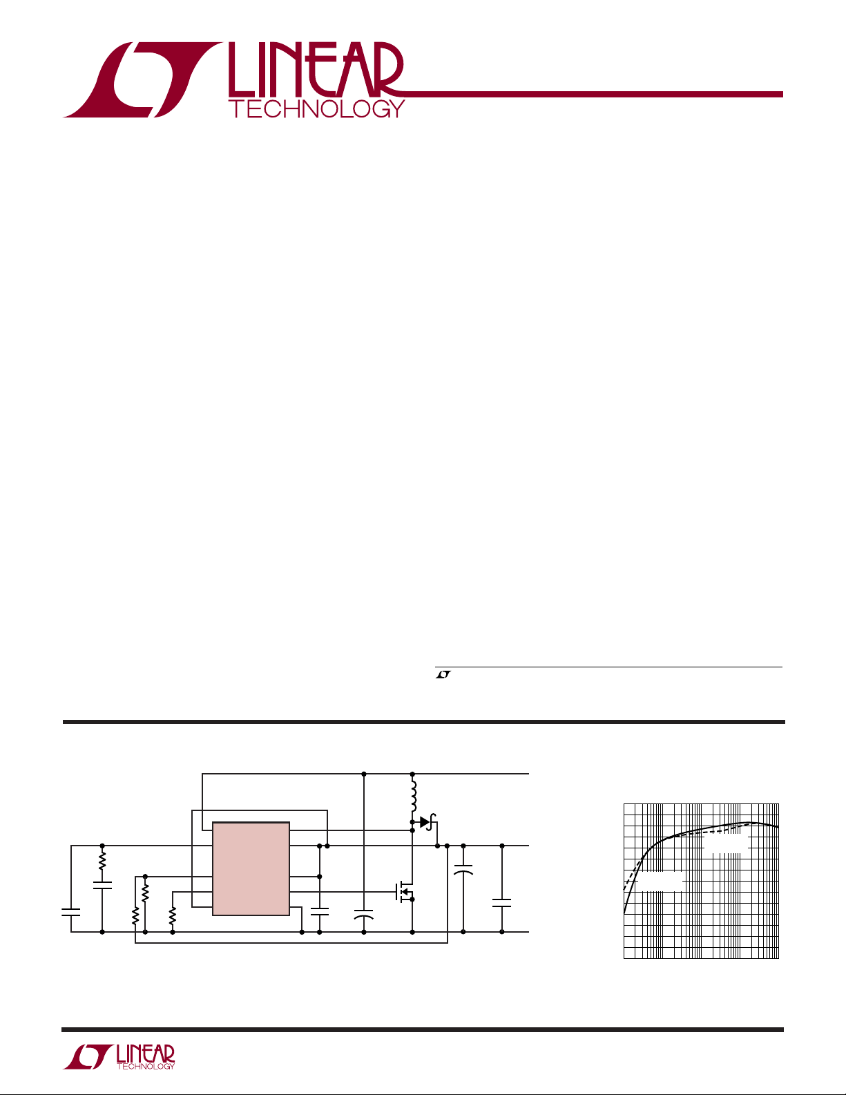
OSC
Wide Input Range, No R
SENSE
Current Mode Boost,
Flyback and SEPIC Controller
U
DESCRIPTIO
The LTC®1871 is a wide input range, current mode, boost,
flyback or SEPIC controller that drives an N-channel
power MOSFET and requires very few external components. Intended for low to medium power applications, it
eliminates the need for a current sense resistor by utilizing the power MOSFET’s on-resistance, thereby maximizing efficiency.
The IC’s operating frequency can be set with an external
resistor over a 50kHz to 1MHz range, and can be synchronized to an external clock using the MODE/SYNC pin.
Burst Mode operation at light loads, a low minimum
operating supply voltage of 2.5V and a low shutdown
quiescent current of 10µA make the LTC1871 ideally
suited for battery-operated systems.
For applications requiring constant frequency operation,
Burst Mode operation can be defeated using the MODE/
SYNC pin. Higher output voltage boost, SEPIC and flyback applications are possible with the LTC1871 by
connecting the SENSE pin to a resistor in the source of the
power MOSFET.
The LTC1871 is available in the 10-lead MSOP package.
, LTC and LT are registered trademarks of Linear Technology Corporation.
TM
Burst Mode is a registered trademark of Linear Technology Corporation. No R
of Linear Technology Corporation. All other trademarks are the property of their respective owners.
is a trademark
SENSE
TYPICAL APPLICATIO
RUN
I
R
T
80.6k
1%
TH
LTC1871
FB
FREQ
MODE/SYNC
R
C
22k
C
R1
C1
6.8nF
12.1k
1%
R2
C
C2
37.4k
47pF
1%
CIN: TAIYO YUDEN JMK325BJ226MM
: PANASONIC EEFUEOJ151R
C
OUT1
: TAIYO YUDEN JMK325BJ226MM
C
OUT2
Figure 1. High Efficiency 3.3V Input, 5V Output Boost Converter (Bootstrapped)
U
SENSE
V
IN
INTV
CC
GATE
GND
D1: MBRB2515L
L1: SUMIDA CEP125-H 1R0MH
M1: FAIRCHILD FDS7760A
C
VCC
4.7µF
X5R
V
IN
C
22µF
6.3V
X5R
×2
1871 F01a
3.3V
V
5V
7A
(10A PEAK)
OUT2
GND
OUT
EFFICIENCY (%)
L1
1µH
D1
C
OUT1
+
150µF
6.3V
M1
C
IN
+
22µF
6.3V
×2
×4
Efficiency of Figure 1
100
90
80
70
PULSE-SKIP
MODE
60
50
40
30
0.01
0.001 0.1 1 10
OUTPUT CURRENT (A)
Burst Mode
OPERATION
1871 F01b
1871fc
1
Page 2
LTC1871
1
2
3
4
5
RUN
I
TH
FB
FREQ
MODE/
SYNC
10
9
8
7
6
SENSE
V
IN
INTV
CC
GATE
GND
TOP VIEW
MS PACKAGE
10-LEAD PLASTIC MSOP
WWWU
ABSOLUTE AXI U RATI GS
PACKAGE/ORDER I FOR ATIO
UU
W
(Note 1)
VIN Voltage ............................................... –0.3V to 36V
INTV
INTV
GATE Voltage ........................... – 0.3V to V
I
RUN, MODE/SYNC Voltages ....................... –0.3V to 7V
Voltage ........................................... –0.3V to 7V
CC
Output Current ........................................ 50mA
CC
+ 0.3V
INTVCC
, FB Voltages ....................................... – 0.3V to 2.7V
TH
T
= 125°C, θJA = 120°C/ W
JMAX
FREQ Voltage ............................................– 0.3V to 1.5V
SENSE Pin Voltage ................................... – 0.3V to 36V
Operating Junction Temperature Range (Note 2)
LTC1871E ........................................... – 40°C to 85°C
LTC1871I.......................................... – 40°C to 125°C
Junction Temperature (Note 3)............................ 125°C
Storage Temperature Range ................. –65°C to 150°C
Lead Temperature (Soldering, 10 sec).................. 300°C
ELECTRICAL CHARACTERISTICS
range, otherwise specifications are at TA = 25°C. VIN = V
SYMBOL PARAMETER CONDITIONS MIN TYP MAX UNITS
Main Control Loop
V
IN(MIN)
I
Q
+
V
RUN
–
V
RUN
V
RUN(HYST)
I
RUN
V
FB
I
FB
∆V
FB
∆V
IN
2
Minimum Input Voltage 2.5 V
Input Voltage Supply Current (Note 4)
Continuous Mode V
Burst Mode Operation, No Load V
Shutdown Mode V
Rising RUN Input Threshold Voltage 1.348 V
Falling RUN Input Threshold Voltage 1.223 1.248 1.273 V
RUN Pin Input Threshold Hysteresis 50 100 150 mV
RUN Input Current 160 nA
Feedback Voltage V
FB Pin Input Current V
Line Regulation 2.5V ≤ VIN ≤ 30V 0.002 0.02 %/V
The ● denotes specifications which apply over the full operating temperature
= 5V, V
INTVCC
I-Grade (Note 2)
MODE/SYNC
V
MODE/SYNC
I-Grade (Note 2)
MODE/SYNC
V
MODE/SYNC
I-Grade (Note 2)
RUN
V
RUN
I-Grade (Note 2)
ITH
V
ITH
ITH
2.5V ≤ VIN ≤ 30V, I-Grade (Note 2)
= 5V, VFB = 1.4V, V
= 5V, VFB = 1.4V, V
= 0V, V
= 0V, V
= 0V 10 20 µA
= 0V, I-Grade (Note 2)
= 0.2V (Note 5) 1.218 1.230 1.242 V
= 0.2V (Note 5), I-Grade (Note 2)
= 0.2V (Note 5) 18 60 nA
ORDER PART NUMBER
LTC1871EMS
LTC1871IMS
Order Options Tape and Reel: Add #TR
Lead Free: Add #PBF Lead Free Tape and Reel: Add #TRPBF
Lead Free Part Marking: http://www.linear.com/leadfree/
Consult LTC Marketing for parts specified with wider operating temperature ranges.
= 1.5V, R
RUN
= 0.2V (Note 5) 250 500 µA
ITH
= 0.2V (Note 5),
ITH
= 80k, V
FREQ
= 0.75V 550 1000 µA
ITH
= 0.75V,
ITH
MODE/SYNC
●
●
●
●
●
●
●
●
●
MS PART MARKING
LTSX
LTBFC
= 0V, unless otherwise specified.
2.5 V
550 1000 µA
250 500 µA
10 20 µA
1.198 1.298 V
35 100 175 mV
1.212 1.248 V
1.205 1.255 V
0.002 0.02 %/V
1871fc
Page 3
LTC1871
ELECTRICAL CHARACTERISTICS
range, otherwise specifications are at T
= 25°C. VIN = V
A
The ● denotes specifications which apply over the full operating temperature
INTVCC
= 5V, V
= 1.5V, R
RUN
FREQ
= 80k, V
MODE/SYNC
= 0V, unless otherwise specified.
SYMBOL PARAMETER CONDITIONS MIN TYP MAX UNITS
∆V
∆V
FB
ITH
Load Regulation V
MODE/SYNC
V
MODE/SYNC
= 0V, V
= 0V, V
= 0.5V to 0.9V (Note 5)
ITH
= 0.5V to 0.9V (Note 5)
ITH
●
–1 –0.1 %
●
–1 –0.1 %
I-Grade (Note 2)
∆V
FB(OV)
g
m
V
ITH(BURST)
V
SENSE(MAX)
I
SENSE(ON)
I
SENSE(OFF)
∆FB Pin, Overvoltage Lockout V
FB(OV)
– V
in Percent 2.5 6 10 %
FB(NOM)
Error Amplifier Transconductance ITH Pin Load = ±5µA (Note 5) 650 µmho
Burst Mode Operation ITH Pin Voltage Falling ITH Voltage (Note 5) 0.3 V
Maximum Current Sense Input Threshold Duty Cycle < 20% 120 150 180 mV
SENSE Pin Current (GATE High) V
SENSE Pin Current (GATE Low) V
Duty Cycle < 20%, I-Grade (Note 2)
= 0V 35 50 µA
SENSE
= 30V 0.1 5 µA
SENSE
●
100 200 mV
Oscillator
f
OSC
Oscillator Frequency R
= 80k 250 300 350 kHz
FREQ
R
= 80k, I-Grade (Note 2)
FREQ
●
250 300 350 kHz
Oscillator Frequency Range 50 1000 kHz
D
MAX
f
SYNC/fOSC
I-Grade (Note 2)
Maximum Duty Cycle 87 92 97 %
I-Grade (Note 2)
Recommended Maximum Synchronized f
= 300kHz (Note 6) 1.25 1.30
OSC
●
50 1000 kHz
●
87 92 97 %
Frequency Ratio
f
t
SYNC(MIN)
t
SYNC(MAX)
V
IL(MODE)
V
IH(MODE)
R
MODE/SYNC
V
FREQ
= 300kHz (Note 6), I-Grade (Note 2)
OSC
MODE/SYNC Minimum Input Pulse Width V
MODE/SYNC Maximum Input Pulse Width V
= 0V to 5V 25 ns
SYNC
= 0V to 5V 0.8/f
SYNC
Low Level MODE/SYNC Input Voltage 0.3 V
I-Grade (Note 2)
High Level MODE/SYNC Input Voltage 1.2 V
I-Grade (Note 2)
MODE/SYNC Input Pull-Down Resistance 50 kΩ
Nominal FREQ Pin Voltage 0.62 V
●
●
●
1.2 V
1.25 1.30
OSC
0.3 V
ns
Low Dropout Regulator
V
INTVCC
∆V
INTVCC
∆V
IN1
∆V
INTVCC
∆V
IN2
V
LDO(LOAD)
V
DROPOUT
I
INTVCC
INTVCC Regulator Output Voltage VIN = 7.5V 5.0 5.2 5.4 V
VIN = 7.5V, I-Grade (Note 2)
●
5.0 5.2 5.4 V
INTVCC Regulator Line Regulation 7.5V ≤ VIN ≤ 15V 8 25 mV
INTVCC Regulator Line Regulation 15V ≤ VIN ≤ 30V 70 200 mV
INTVCC Load Regulation 0 ≤ I
≤ 20mA, VIN = 7.5V –2 –0.2 %
INTVCC
INTVCC Regulator Dropout Voltage VIN = 5V, INTVCC Load = 20mA 280 mV
Bootstrap Mode INTVCC Supply RUN = 0V, SENSE = 5V 10 20 µA
Current in Shutdown
I-Grade (Note 2)
●
30 µA
GATE Driver
t
r
t
f
GATE Driver Output Rise Time CL = 3300pF (Note 7) 17 100 ns
GATE Driver Output Fall Time CL = 3300pF (Note 7) 8 100 ns
1871fc
3
Page 4
LTC1871
ELECTRICAL CHARACTERISTICS
range, otherwise specifications are at T
Note 1: Absolute Maximum Ratings are those values beyond which the life
of the device may be impaired.
Note 2: The LTC1871E is guaranteed to meet performance specifications
from 0°C to 70°C junction temperature. Specifications over the –40°C to
85°C operating junction temperature range are assured by design,
characterization and correlation with statistical process controls. The
LTC1871I is guaranteed over the full –40°C to 125°C operating junction
temperature range.
Note 3: T
dissipation P
is calculated from the ambient temperature TA and power
J
according to the following formula:
D
= TA + (PD • 110°C/W)
T
J
= 25°C. VIN = V
A
The ● denotes specifications which apply over the full operating temperature
INTVCC
= 5V, V
= 1.5V, R
RUN
FREQ
= 80k, V
MODE/SYNC
= 0V, unless otherwise specified.
Note 4: The dynamic input supply current is higher due to power MOSFET
gate charging (Q
• f
). See Applications Information.
G
OSC
Note 5: The LTC1871 is tested in a feedback loop which servos V
reference voltage with the I
range (0.3V ≤ V
≤ 1.2V, midpoint = 0.75V).
ITH
pin forced to the midpoint of its voltage
TH
Note 6: In a synchronized application, the internal slope compensation
gain is increased by 25%. Synchronizing to a significantly higher ratio will
reduce the effective amount of slope compensation, which could result in
subharmonic oscillation for duty cycles greater than 50%.
Note 7: Rise and fall times are measured at 10% and 90% levels.
UW
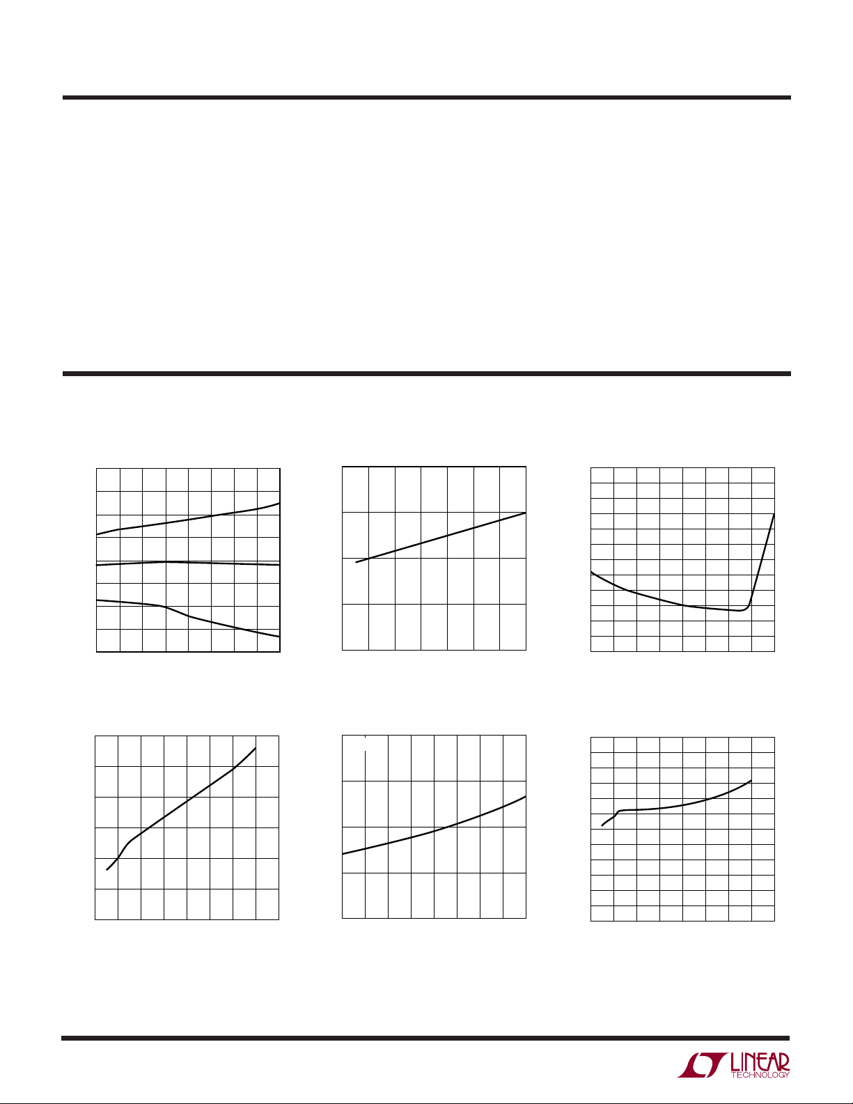
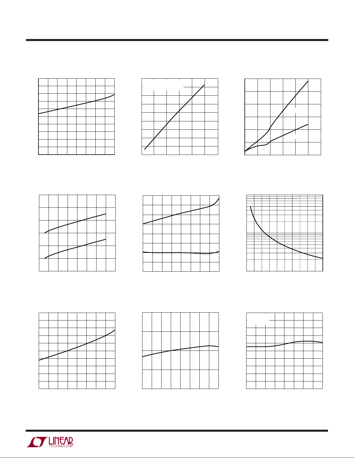
TYPICAL PERFOR A CE CHARACTERISTICS
FB Voltage vs Temp FB Voltage Line Regulation FB Pin Current vs Temperature
1.25
1.24
1.231
60
50
40
to the
FB
1.23
FB VOLTAGE (V)
1.22
1.21
–25
–50
0
TEMPERATURE (°C)
Shutdown Mode IQ vs V
30
(µA)
Q
20
10
SHUTDOWN MODE I
0
0
10 20
25
50
VIN (V)
1.230
FB VOLTAGE (V)
75
100
IN
30
125
1871 G01
150
1871 G04
1.229
(µA)
Q
SHUTDOWN MODE I
40
5101520
0
VIN (V)
25 30 35
Shutdown Mode IQ vs Temperature
20
VIN = 5V
15
10
5
0
–50
–25 0 25 50
TEMPERATURE (°C)
75 100 125 150
1871 G02
1871 G05
30
20
FB PIN CURRENT (nA)
10
0
–50
–25
Burst Mode IQ vs V
600
500
400
(µA)
Q
300
200
Burst Mode I
100
0
0
10 20
250 50 10075
TEMPERATURE (°C)
IN
VIN (V)
125 150
1871 G03
30 40
1871 G06
4
1871fc
Page 5
UW
TEMPERATURE (°C)
–50
25
SENSE PIN CURRENT (µA)
30
35
0
50
75
1871 G15
–25 25
100
125
150
GATE HIGH
V
SENSE
= 0V
TYPICAL PERFOR A CE CHARACTERISTICS
Burst Mode IQ vs Temperature
500
400
(µA)
300
Q
200
Burst Mode I
100
0
–50
–25 25
0
50
TEMPERATURE (°C)
125
100
75
150
1871 G07
Dynamic IQ vs Frequency
18
CL = 3300pF
= 550µA + Qg • f
I
16
Q(TOT)
14
12
10
(mA)
Q
8
I
6
4
2
0
0
400 1200
200 1000
FREQUENCY (kHz)
600
800
1871 G08
LTC1871
Gate Drive Rise and Fall Time
vs C
L
60
50
40
RISE TIME
30
TIME (ns)
20
10
0
0
4000 6000 8000
2000
FALL TIME
CL (pF)
10000 12000
1871 G09
RUN Thresholds vs V
1.5
1.4
1.3
RUN THRESHOLDS (V)
1.2
0
Frequency vs Temperature
325
320
315
310
305
300
295
290
GATE FREQUENCY (kHz)
285
280
275
–50
10 20
–25 25
0
TEMPERATURE (°C)
VIN (V)
50
IN
30
40
1871 G10
RUN Thresholds vs Temperature
1.40
1.35
1.30
RUN THRESHOLDS (V)
1.25
1.20
–50
–25
0
50
25
TEMPERATURE (°C)
75
100
125
1871 G11
150
RT vs Frequency
1000
100
(kΩ)
T
R
10
100
0
200 1000
400
500
300
FREQUENCY (kHz)
800700600
900
1871 G12
Maximum Sense Threshold
vs Temperature
160
155
150
145
MAX SENSE THRESHOLD (mV)
140
–50
125
100
75
150
1871 G13
–25 0 25 50
TEMPERATURE (°C)
75 100 125 150
1871 G14
SENSE Pin Current vs Temperature
1871fc
5
Page 6
LTC1871
UW
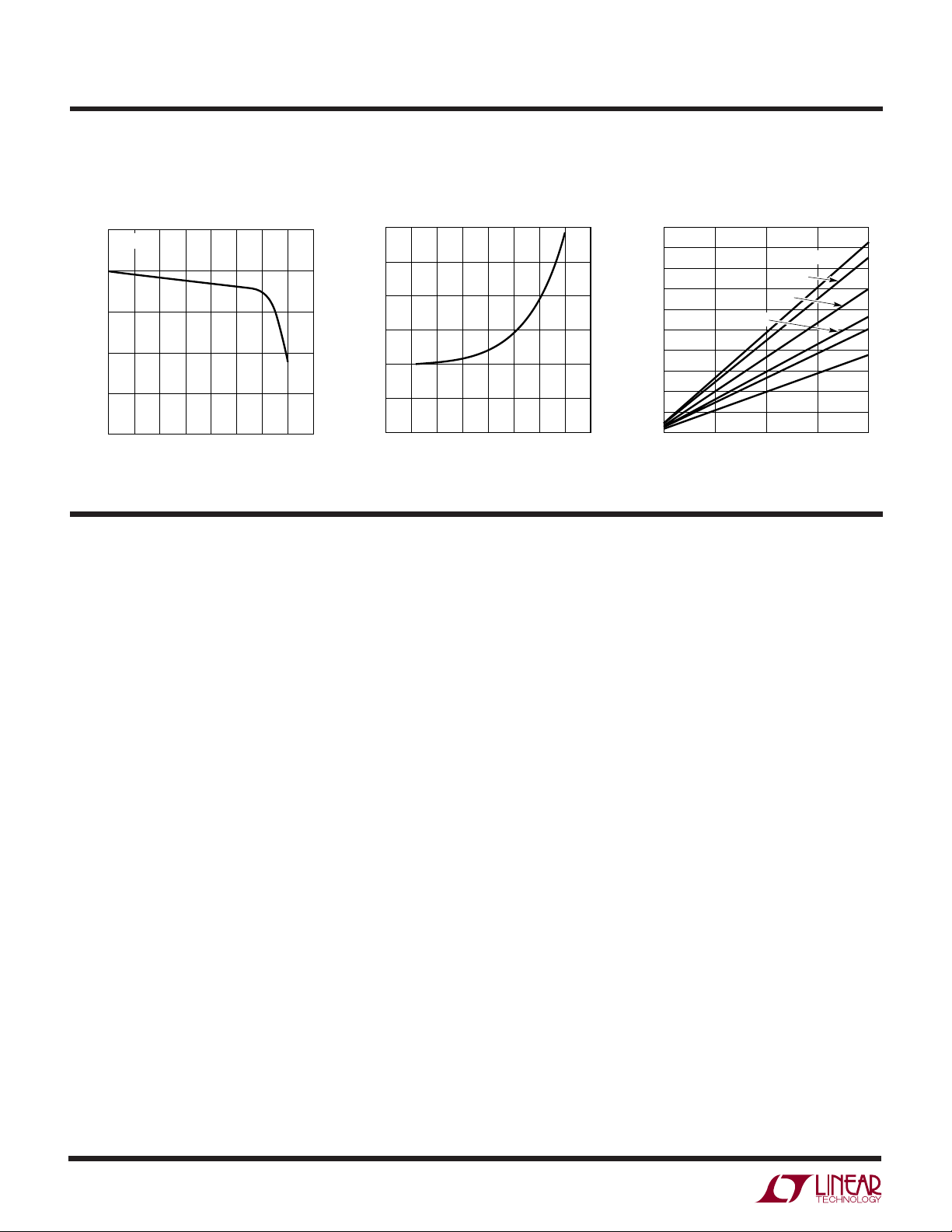
TYPICAL PERFOR A CE CHARACTERISTICS
INTVCC Load Regulation
VIN = 7.5V
5.2
VOLTAGE (V)
CC
5.1
INTV
5.0
0
10 20
30 50 80
INTVCC LOAD (mA)
40
60 70
1871 G16
INTV
5.4
5.3
VOLTAGE (V)
CC
5.2
INTV
5.1
0
Line Regulation
CC
515
10 20
VIN (V)
25
30
35
1871 G17
INTV
Dropout Voltage
CC
vs Current, Temperature
500
450
400
350
300
250
200
150
DROPOUT VOLTAGE (mV)
100
50
40
0
0
25°C
5
10
INTVCC LOAD (mA)
125°C
75°C
150°C
–50°C
15
0°C
20
1871 G18
U
UU
PI FU CTIO S
RUN (Pin 1): The RUN pin provides the user with an
accurate means for sensing the input voltage and programming the start-up threshold for the converter. The
falling RUN pin threshold is nominally 1.248V and the
comparator has 100mV of hysteresis for noise immunity.
When the RUN pin is below this input threshold, the IC is
shut down and the V
value (typ 10µA). The Absolute Maximum Rating for the
voltage on this pin is 7V.
I
(Pin 2): Error Amplifier Compensation Pin. The cur-
TH
rent comparator input threshold increases with this
control voltage. Nominal voltage range for this pin is 0V
to 1.40V.
FB (Pin 3): Receives the feedback voltage from the
external resistor divider across the output. Nominal
voltage for this pin in regulation is 1.230V.
FREQ (Pin 4): A resistor from the FREQ pin to ground
programs the operating frequency of the chip. The nominal voltage at the FREQ pin is 0.6V.
MODE/SYNC (Pin 5): This input controls the operating
mode of the converter and allows for synchronizing the
supply current is kept to a low
IN
operating frequency to an external clock. If the MODE/
SYNC pin is connected to ground, Burst Mode operation
is enabled. If the MODE/SYNC pin is connected to INTV
, or if an external logic-level synchronization signal
CC
is applied to this input, Burst Mode operation is disabled
and the IC operates in a continuous mode.
GND (Pin 6): Ground Pin.
GATE (Pin 7): Gate Driver Output.
I
NTVCC (Pin 8): The Internal 5.20V Regulator Output. The
gate driver and control circuits are powered from this
voltage. Decouple this pin locally to the IC ground with a
minimum of 4.7µF low ESR tantalum or ceramic
capacitor.
V
(Pin 9): Main Supply Pin. Must be closely decoupled
IN
to ground.
SENSE (Pin 10): The Current Sense Input for the Control
Loop. Connect this pin to the drain of the power MOSFET
for V
sensing and highest efficiency. Alternatively, the
DS
SENSE pin may be connected to a resistor in the source
of the power MOSFET. Internal leading edge blanking is
provided for both sensing methods.
6
1871fc
Page 7
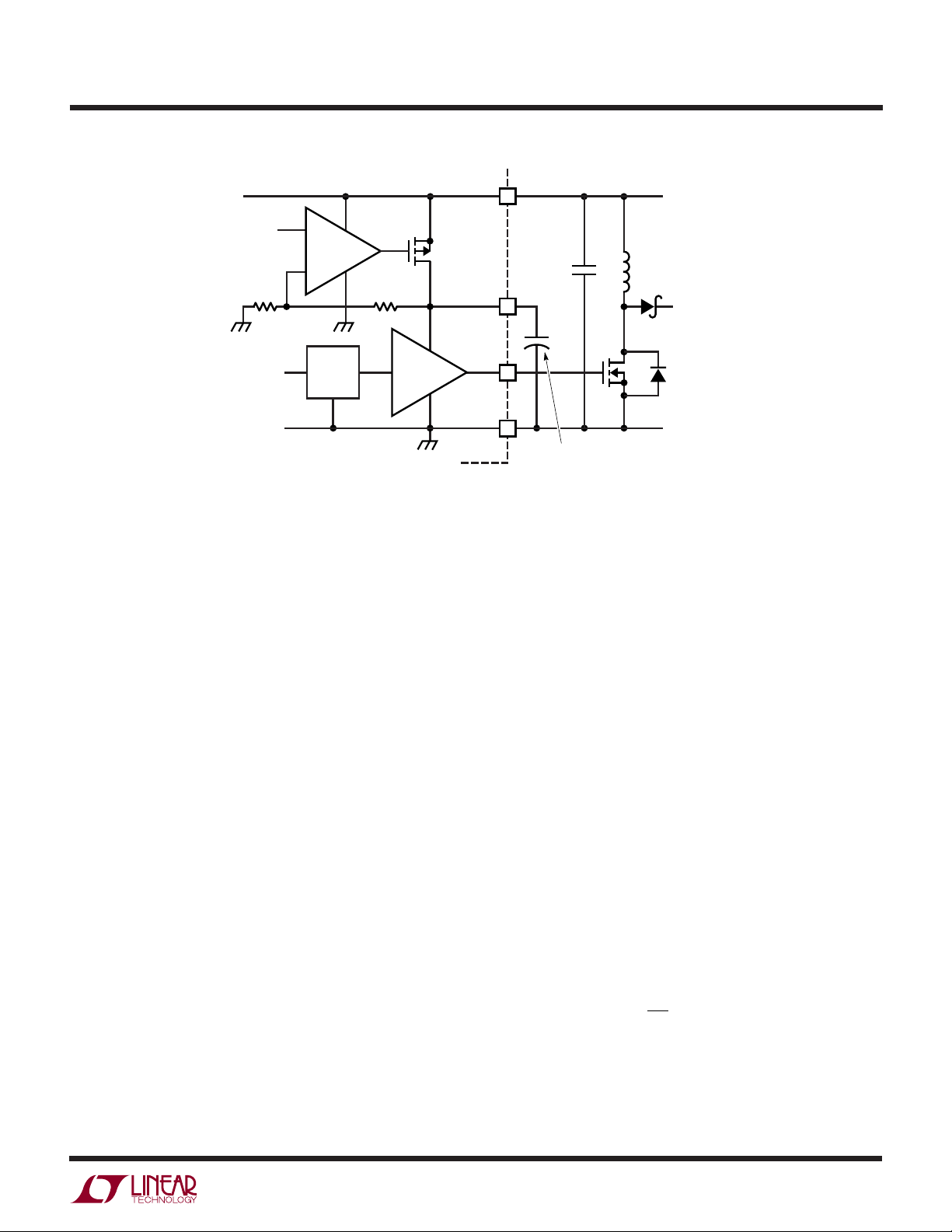
BLOCK DIAGRA
W
SLOPE
COMPENSATION
BIAS AND
START-UP
CONTROL
LTC1871
RUN
1
+
C2
1.248V
–
FREQ
4
MODE/SYNC
5
85mV
1.230V
FB
3
1.230V
I
TH
2
INTV
CC
8
2.00V
V
IN
0.6V
OV
–
+
I
OSC
50k
+
+
–
1.230V
TO
START-UP
CONTROL
5.2V
0.30V
EA
–
g
m
+
LDO
UV
–
+
OSCV-TO-I
BURST
COMPARATOR
V-TO-I
SLOPE
BIAS V
I
LOOP
1.230V
REF
PWM LATCH
S
Q
R
CURRENT
COMPARATOR
INTV
LOGIC
+
C1
–
GND
R
9
CC
GATE
7
SENSE
10
LOOP
GND
6
1871 BD
V
IN
1871fc
7
Page 8

LTC1871
OPERATIO
U
Main Control Loop
The LTC1871 is a constant frequency, current mode
controller for DC/DC boost, SEPIC and flyback converter
applications. The LTC1871 is distinguished from conventional current mode controllers because the current control loop can be closed by sensing the voltage drop across
the power MOSFET switch instead of across a discrete
sense resistor, as shown in Figure 2. This sensing technique improves efficiency, increases power density, and
reduces the cost of the overall solution.
D
V
OUT
+
C
V
SW
V
SW
R
OUT
D
V
OUT
+
C
OUT
S
1871 F02
V
IN
SENSE
GATE
GND
V
IN
GATE
SENSE
GND
L
L
V
IN
GND
2a. SENSE Pin Connection for
Maximum Efficiency (VSW < 36V)
V
IN
GND
2b. SENSE Pin Connection for Precise
Control of Peak Current or for VSW > 36V
Figure 2. Using the SENSE Pin On the LTC1871
to rise, which causes the current comparator C1 to trip at
a higher peak inductor current value. The average inductor
current will therefore rise until it equals the load current,
thereby maintaining output regulation.
The nominal operating frequency of the LTC1871 is programmed using a resistor from the FREQ pin to ground
and can be controlled over a 50kHz to 1000kHz range. In
addition, the internal oscillator can be synchronized to an
external clock applied to the MODE/SYNC pin and can be
locked to a frequency between 100% and 130% of its
nominal value. When the MODE/SYNC pin is left open, it is
pulled low by an internal 50k resistor and Burst Mode
operation is enabled. If this pin is taken above 2V or an
external clock is applied, Burst Mode operation is disabled
and the IC operates in continuous mode. With no load (or
an extremely light load), the controller will skip pulses in
order to maintain regulation and prevent excessive output
ripple.
The RUN pin controls whether the IC is enabled or is in a
low current shutdown state. A micropower 1.248V reference and comparator C2 allow the user to program the
supply voltage at which the IC turns on and off (comparator C2 has 100mV of hysteresis for noise immunity). With
the RUN pin below 1.248V, the chip is off and the input
supply current is typically only 10µA.
An overvoltage comparator OV senses when the FB pin
exceeds the reference voltage by 6.5% and provides a
reset pulse to the main RS latch. Because this RS latch is
reset-dominant, the power MOSFET is actively held off for
the duration of an output overvoltage condition.
For circuit operation, please refer to the Block Diagram of
the IC and Figure 1. In normal operation, the power
MOSFET is turned on when the oscillator sets the PWM
latch and is turned off when the current comparator C1
resets the latch. The divided-down output voltage is compared to an internal 1.230V reference by the error amplifier
EA, which outputs an error signal at the ITH pin. The voltage
on the I
pin sets the current comparator C1 input
TH
threshold. When the load current increases, a fall in the FB
voltage relative to the reference voltage causes the I
TH
pin
8
The LTC1871 can be used either by sensing the voltage
drop across the power MOSFET or by connecting the
SENSE pin to a conventional shunt resistor in the source
of the power MOSFET, as shown in Figure 2. Sensing the
voltage across the power MOSFET maximizes converter
efficiency and minimizes the component count, but limits
the output voltage to the maximum rating for this pin
(36V). By connecting the SENSE pin to a resistor in the
source of the power MOSFET, the user is able to program
output voltages significantly greater than 36V.
1871fc
Page 9
OPERATIO
LTC1871
U
Programming the Operating Mode
For applications where maximizing the efficiency at very
light loads (e.g., <100µA) is a high priority, the current in
the output divider could be decreased to a few microamps and Burst Mode operation should be applied (i.e.,
the MODE/SYNC pin should be connected to ground). In
applications where fixed frequency operation is more
critical than low current efficiency, or where the lowest
output ripple is desired, pulse-skip mode operation should
be used and the MODE/SYNC pin should be connected to
the INTVCC pin. This allows discontinuous conduction
mode (DCM) operation down to near the limit defined by
the chip’s minimum on-time (about 175ns). Below this
output current level, the converter will begin to skip
cycles in order to maintain output regulation. Figures 3
and 4 show the light load switching waveforms for Burst
Mode and pulse-skip mode operation for the converter in
Figure 1.
Burst Mode Operation
Burst Mode operation is selected by leaving the MODE/
SYNC pin unconnected or by connecting it to ground. In
normal operation, the range on the ITH pin corresponding
to no load to full load is 0.30V to 1.2V. In Burst Mode
operation, if the error amplifier EA drives the I
below 0.525V, the buffered I
input to the current com-
TH
voltage
TH
parator C1 will be clamped at 0.525V (which corresponds
to 25% of maximum load current). The inductor current
peak is then held at approximately 30mV divided by the
power MOSFET R
. If the ITH pin drops below 0.30V,
DS(ON)
the Burst Mode comparator B1 will turn off the power
MOSFET and scale back the quiescent current of the IC to
250µA (sleep mode). In this condition, the load current will
be supplied by the output capacitor until the I
voltage
TH
rises above the 50mV hysteresis of the burst comparator.
At light loads, short bursts of switching (where the average inductor current is 20% of its maximum value) followed by long periods of sleep will be observed, thereby
greatly improving converter efficiency. Oscilloscope waveforms illustrating Burst Mode operation are shown in
Figure 3.
Pulse-Skip Mode Operation
With the MODE/SYNC pin tied to a DC voltage above 2V,
Burst Mode operation is disabled. The internal, 0.525V
buffered I
burst clamp is removed, allowing the ITH pin
TH
to directly control the current comparator from no load to
full load. With no load, the I
pin is driven below 0.30V,
TH
the power MOSFET is turned off and sleep mode is
invoked. Oscilloscope waveforms illustrating this mode of
operation are shown in Figure 4.
When an external clock signal drives the MODE/SYNC pin
at a rate faster than the chip’s internal oscillator, the
oscillator will synchronize to it. In this synchronized mode,
Burst Mode operation is disabled. The constant frequency
associated with synchronized operation provides a more
controlled noise spectrum from the converter, at the
expense of overall system efficiency of light loads.
VIN = 3.3V
= 5V
V
OUT
= 500mA
I
OUT
V
OUT
50mV/DIV
I
L
5A/DIV
Figure 3. LTC1871 Burst Mode Operation
(MODE/SYNC = 0V) at Low Output Current
MODE/SYNC = 0V
(Burst Mode OPERATION)
10µs/DIV 1871 F03
VIN = 3.3V
= 5V
V
OUT
= 500mA
I
OUT
V
OUT
50mV/DIV
I
L
5A/DIV
Figure 4. LTC1871 Low Output Current Operation with Burst
Mode Operation Disabled (MODE/SYNC = INTV
MODE/SYNC = INTV
(PULSE-SKIP MODE)
2µs/DIV
CC
1871 F04
)
CC
1871fc
9
Page 10
LTC1871
WUUU
APPLICATIO S I FOR ATIO
When the oscillator’s internal logic circuitry detects a
synchronizing signal on the MODE/SYNC pin, the internal
oscillator ramp is terminated early and the slope compensation is increased by approximately 30%. As a result, in
applications requiring synchronization, it is recommended
that the nominal operating frequency of the IC be programmed to be about 75% of the external clock frequency.
Attempting to synchronize to too high an external frequency (above 1.3f
) can result in inadequate slope com-
O
pensation and possible subharmonic oscillation (or jitter).
The external clock signal must exceed 2V for at least 25ns,
and should have a maximum duty cycle of 80%, as shown
in Figure 5. The MOSFET turn on will synchronize to the
rising edge of the external clock signal.
MODE/
SYNC
GATE
I
L
Figure 5. MODE/SYNC Clock Input and Switching
Waveforms for Synchronized Operation
t
MIN
= 25ns
D = 40%
0.8T
T T = 1/f
2V TO 7V
O
1871 F05
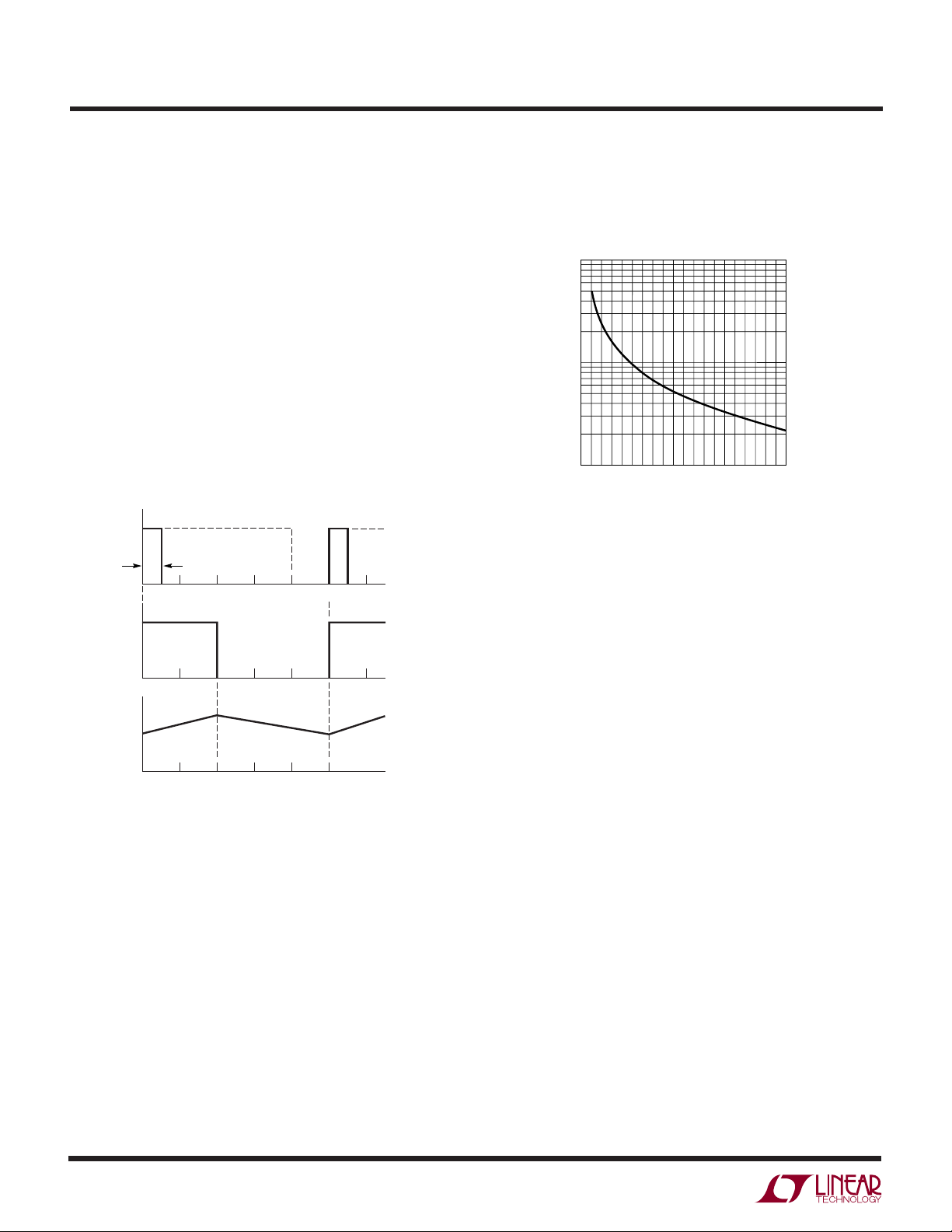
Programming the Operating Frequency
The choice of operating frequency and inductor value is a
tradeoff between efficiency and component size. Low
frequency operation improves efficiency by reducing
MOSFET and diode switching losses. However, lower
frequency operation requires more inductance for a given
amount of load current.
The LTC1871 uses a constant frequency architecture that
can be programmed over a 50kHz to 1000kHz range with
a single external resistor from the FREQ pin to ground, as
shown in Figure 1. The nominal voltage on the FREQ pin is
0.6V, and the current that flows into the FREQ pin is used
to charge and discharge an internal oscillator capacitor. A
graph for selecting the value of R
for a given operating
T
frequency is shown in Figure 6.
1000
100
(kΩ)
T
R
INTV
10
Regulator Bypassing and Operation
CC
200 1000
100
0
Figure 6. Timing Resistor (RT) Value
400
500
300
FREQUENCY (kHz)
800700600
900
1871 F06
An internal, P-channel low dropout voltage regulator produces the 5.2V supply which powers the gate driver and
logic circuitry within the LTC1871, as shown in Figure 7.
The INTV
regulator can supply up to 50mA and must be
CC
bypassed to ground immediately adjacent to the IC pins
with a minimum of 4.7µF tantalum or ceramic capacitor.
Good bypassing is necessary to supply the high transient
currents required by the MOSFET gate driver.
For input voltages that don’t exceed 7V (the absolute
maximum rating for this pin), the internal low dropout
regulator in the LTC1871 is redundant and the INTV
can be shorted directly to the V
pin. With the INTVCC pin
IN
CC
pin
shorted to VIN, however, the divider that programs the
regulated INTV
voltage will draw 10µA of current from
CC
the input supply, even in shutdown mode. For applications
that require the lowest shutdown mode input supply
current, do not connect the INTVCC pin to VIN. Regardless
of whether the INTV
pin is shorted to VIN or not, it is
CC
always necessary to have the driver circuitry bypassed
with a 4.7µF tantalum or low ESR ceramic capacitor to
ground immediately adjacent to the INTVCC and GND
pins.
In an actual application, most of the IC supply current is
used to drive the gate capacitance of the power MOSFET.
1871fc
10
Page 11
WUUU
APPLICATIO S I FOR ATIO
LTC1871
1.230V
R2
–
DRIVER
P-CH
5.2V
INTV
+
R1
LOGIC
Figure 7. Bypassing the LDO Regulator and Gate Driver Supply
As a result, high input voltage applications in which a large
power MOSFET is being driven at high frequencies can
cause the LTC1871 to exceed its maximum junction
temperature rating. The junction temperature can be
estimated using the following equations:
I
≈ IQ + f • Q
Q(TOT)
G
PIC = VIN • (IQ + f • QG)
= TA + PIC • R
T
J
The total quiescent current I
supply current (I
TH(JA)
consists of the static
Q(TOT)
) and the current required to charge and
Q
discharge the gate of the power MOSFET. The 10-pin
MSOP package has a thermal resistance of R
TH(JA)
=
120°C/W.
As an example, consider a power supply with V
V
= 12V at IO = 1A. The switching frequency is 500kHz,
O
= 5V and
IN
and the maximum ambient temperature is 70°C. The
power MOSFET chosen is the IRF7805, which has a
maximum R
of 11mΩ (at room temperature) and a
DS(ON)
maximum total gate charge of 37nC (the temperature
coefficient of the gate charge is low).
= 600µA + 37nC • 500kHz = 19.1mA
I
Q(TOT)
P
= 5V • 19.1mA = 95mW
IC
= 70°C + 120°C/W • 95mW = 81.4°C
T
J
V
GATE
GND
IN
C
IN
CC
+
C
VCC
4.7µF
PLACE AS CLOSE AS
1871 F07
POSSIBLE TO DEVICE PINS
INPUT
SUPPLY
2.5V TO 30V
M1
GND
This demonstrates how significant the gate charge current
can be when compared to the static quiescent current in
the IC.
To prevent the maximum junction temperature from being
exceeded, the input supply current must be checked when
operating in a continuous mode at high V
. A tradeoff
IN
between the operating frequency and the size of the power
MOSFET may need to be made in order to maintain a
reliable IC junction temperature. Prior to lowering the
operating frequency, however, be sure to check with
power MOSFET manufacturers for their latest-and-greatest low QG, low R
devices. Power MOSFET manu-
DS(ON)
facturing technologies are continually improving, with
newer and better performance devices being introduced
almost yearly.
Output Voltage Programming
The output voltage is set by a resistor divider according to
the following formula:
R
2
VV
=+
1 230 1
.•
O
⎛
⎜
⎝
⎞
⎟
⎠
R
1
The external resistor divider is connected to the output as
shown in Figure 1, allowing remote voltage sensing. The
resistors R1 and R2 are typically chosen so that the error
1871fc
11
Page 12

LTC1871
WUUU
APPLICATIO S I FOR ATIO
caused by the current flowing into the FB pin during
normal operation is less than 1% (this translates to a
maximum value of R1 of about 250k).
Programming Turn-On and Turn-Off Thresholds
with the RUN Pin
The LTC1871 contains an independent, micropower voltage reference and comparator detection circuit that remains active even when the device is shut down, as shown
in Figure 8. This allows users to accurately program an
input voltage at which the converter will turn on and off.
The falling threshold voltage on the RUN pin is equal to the
internal reference voltage of 1.248V. The comparator has
100mV of hysteresis to increase noise immunity.
V
IN
RUN
REFERENCE
GND
INPUT
SUPPLY
+
OPTIONAL
FILTER
CAPACITOR
–
R2
R1
The turn-on and turn-off input voltage thresholds are
programmed using a resistor divider according to the
following formulas:
2
R
VV
IN OFF
()
VV
IN ON
()
1 248 1
.•
=+
=
1 348
.•
⎛
⎜
⎝
⎛
11
⎜
⎝
⎞
⎟
⎠
1
R
2
R
⎞
+
⎟
⎠
1
R
The resistor R1 is typically chosen to be less than 1M.
For applications where the RUN pin is only to be used as
a logic input, the user should be aware of the 7V
Absolute Maximum Rating for this pin! The RUN pin can
be connected to the input voltage through an external 1M
resistor, as shown in Figure 8c, for “always on” operation.
RUN
COMPARATOR
6V
1.248V
µPOWER
+
–
BIAS AND
START-UP
CONTROL
1871 F8a
12
Figure 8a. Programming the Turn-On and Turn-Off Thresholds Using the RUN Pin
RUN
COMPARATOR
+
–
1871 F08b
EXTERNAL
LOGIC CONTROL
RUN
6V
1.248V
Figure 8b. On/Off Control Using External Logic
V
IN
RUN
GND
6V
1.248V
INPUT
SUPPLY
+
R2
1M
–
Figure 8c. External Pull-Up Resistor On
RUN Pin for “Always On” Operation
+
–
RUN
COMPARATOR
1871 F08c
1871fc
Page 13

WUUU
APPLICATIO S I FOR ATIO
LTC1871
Application Circuits
A basic LTC1871 application circuit is shown in
Figure 1. External component selection is driven by the
characteristics of the load and the input supply. The first
topology to be analyzed will be the boost converter,
followed by SEPIC (single ended primary inductance
converter).
Boost Converter: Duty Cycle Considerations
For a boost converter operating in a continuous conduction mode (CCM), the duty cycle of the main switch is:
⎛
VVV
D
ODIN
=
⎜
⎝
+
VV
+
OD
⎞
–
⎟
⎠
where VD is the forward voltage of the boost diode. For
converters where the input voltage is close to the output
voltage, the duty cycle is low and for converters that
develop a high output voltage from a low voltage input
supply, the duty cycle is high. The maximum output
voltage for a boost converter operating in CCM is:
V
()
V
OMAX
IN MIN
D
–
1
()
MAX
V
–=
D()
The maximum duty cycle capability of the LTC1871 is
typically 92%. This allows the user to obtain high output
voltages from low input supply voltages.
Boost Converter: The Peak and Average Input Currents
The control circuit in the LTC1871 is measuring the input
current (either by using the R
of the power MOSFET
DS(ON)
or by using a sense resistor in the MOSFET source), so the
output current needs to be reflected back to the input in
order to dimension the power MOSFET properly. Based on
the fact that, ideally, the output power is equal to the input
power, the maximum average input current is:
I
OMAX
()
I
IN MAX
The peak input current is
I
IN PEAK
=
()
()
1
=+
D
–
⎛
1
⎜
⎝
MAX
:
I
χ
⎞
O MAX
•
⎟
⎠
21
–
()
D
MAX
The maximum duty cycle, D
minimum V
IN
.
Boost Converter: Ripple Current ∆I
, should be calculated at
MAX
and the ‘χ’ Factor
L
The constant ‘χ’ in the equation above represents the
percentage peak-to-peak ripple current in the inductor,
relative to its maximum value. For example, if 30% ripple
current is chosen, then χ = 0.30, and the peak current is
15% greater than the average.
For a current mode boost regulator operating in CCM,
slope compensation must be added for duty cycles above
50% in order to avoid subharmonic oscillation. For the
LTC1871, this ramp compensation is internal. Having an
internally fixed ramp compensation waveform, however,
does place some constraints on the value of the inductor
and the operating frequency. If too large an inductor is
used, the resulting current ramp (∆IL) will be small relative
to the internal ramp compensation (at duty cycles above
50%), and the converter operation will approach voltage
mode (ramp compensation reduces the gain of the current
loop). If too small an inductor is used, but the converter is
still operating in CCM (near critical conduction mode), the
internal ramp compensation may be inadequate to prevent
subharmonic oscillation. To ensure good current mode
gain and avoid subharmonic oscillation, it is recommended that the ripple current in the inductor fall in the
range of 20% to 40% of the maximum average current. For
example, if the maximum average input current is 1A,
choose a ∆IL between 0.2A and 0.4A, and a value ‘χ’
between 0.2 and 0.4.
Boost Converter: Inductor Selection
Given an operating input voltage range, and having chosen
the operating frequency and ripple current in the inductor,
the inductor value can be determined using the following
equation:
V
IN MIN
=
I
L
∆
:
()
If
•
L
I
OMAX
()
•–χ
1
•
D
D
MAX
MAX
1871fc
L
where
∆ =
13
Page 14

LTC1871
WUUU
APPLICATIO S I FOR ATIO
Remember that boost converters are not short-circuit
protected. Under a shorted output condition, the inductor
current is limited only by the input supply capability. For
applications requiring a step-up converter that is shortcircuit protected, please refer to the applications section
covering SEPIC converters.
The minimum required saturation current of the inductor
can be expressed as a function of the duty cycle and the
load current, as follows:
I
χ
⎛
⎞
()
I
()
L SAT
≥ +
1
⎜
⎝
OMAX
•
⎟
⎠
D
–
21
MAX
The saturation current rating for the inductor should be
checked at the minimum input voltage (which results in
the highest inductor current) and maximum output
current.
Boost Converter: Operating in Discontinuous Mode
Discontinuous mode operation occurs when the load
current is low enough to allow the inductor current to run
out during the off-time of the switch, as shown in Figure 9.
Once the inductor current is near zero, the switch and
diode capacitances resonate with the inductance to form
damped ringing at 1MHz to 10MHz. If the off-time is long
enough, the drain voltage will settle to the input voltage.
Depending on the input voltage and the residual energy in
the inductor, this ringing can cause the drain of the power
MOSFET to go below ground where it is clamped by the
body diode. This ringing is not harmful to the IC and it has
not been shown to contribute significantly to EMI. Any
attempt to damp it with a snubber will degrade the efficiency.
I
= 5V
= 200mA
OUT
MOSFET DRAIN
VOLTAGE
2V/DIV
VIN = 3.3V
V
OUT
Boost Converter: Inductor Core Selection
Once the value for L is known, the type of inductor must be
selected. High efficiency converters generally cannot afford the core loss found in low cost powdered iron cores,
forcing the use of more expensive ferrite, molypermalloy
®
or Kool Mµ
cores. Actual core loss is independent of core
size for a fixed inductor value, but is very dependent on the
inductance selected. As inductance increases, core losses
go down. Unfortunately, increased inductance requires
more turns of wire and therefore, copper losses will
increase. Generally, there is a tradeoff between core losses
and copper losses that needs to be balanced.
Ferrite designs have very low core losses and are preferred
at high switching frequencies, so design goals can concentrate on copper losses and preventing saturation.
Ferrite core material saturates “hard,” meaning that the
inductance collapses rapidly when the peak design current
is exceeded. This results in an abrupt increase in inductor
ripple current and consequently, output voltage ripple. Do
not allow the core to saturate!
Molypermalloy (from Magnetics, Inc.) is a very good, low
cost core material for toroids, but is more expensive than
ferrite. A reasonable compromise from the same manufacturer is Kool Mµ.
Boost Converter: Power MOSFET Selection
The power MOSFET serves two purposes in the LTC1871:
it represents the main switching element in the power
path, and its R
DS(ON)
represents the current sensing element for the control loop. Important parameters for the
power MOSFET include the drain-to-source breakdown
voltage (BV
resistance (R
gate-to-source and gate-to-drain charges (Q
respectively), the maximum drain current (I
the MOSFET’s thermal resistances (R
), the threshold voltage (V
DSS
) versus gate-to-source voltage, the
DS(ON)
GS(TH)
TH(JC)
), the on-
and QGD,
GS
D(MAX)
and R
) and
TH(JA)
).
INDUCTOR
CURRENT
2A/DIV
14
2µs/DIV
Figure 9. Discontinuous Mode Waveforms
1871 F09
The gate drive voltage is set by the 5.2V INTV
low drop
CC
regulator. Consequently, logic-level threshold MOSFETs
should be used in most LTC1871 applications. If low input
voltage operation is expected (e.g., supplying power from
Kool Mµ is a registered trademark of Magnetics, Inc.
1871fc
Page 15

WUUU
APPLICATIO S I FOR ATIO
LTC1871
a lithium-ion battery or a 3.3V logic supply), then sublogiclevel threshold MOSFETs should be used.
Pay close attention to the BV
specifications for the
DSS
MOSFETs relative to the maximum actual switch voltage in
the application. Many logic-level devices are limited to 30V
or less, and the switch node can ring during the turn-off of
the MOSFET due to layout parasitics. Check the switching
waveforms of the MOSFET directly across the drain and
source terminals using the actual PC board layout (not just
on a lab breadboard!) for excessive ringing.
During the switch on-time, the control circuit limits the
maximum voltage drop across the power MOSFET to
about 150mV (at low duty cycle). The peak inductor
current is therefore limited to 150mV/R
DS(ON)
. The relationship between the maximum load current, duty cycle
and the R
RV
DS ON SENSE MAX
() ( )
The V
SENSE(MAX)
of the power MOSFET is:
DS(ON)
≤
•
term is typically 150mV at low duty
1
D
–
MAX
χ
⎛
⎜
⎝
⎞
1
+
I
••
⎟
O MAX T
()
⎠
2
ρ
cycle, and is reduced to about 100mV at a duty cycle of
92% due to slope compensation, as shown in Figure 10.
The ρT term accounts for the temperature coefficient of
the R
Figure 11 illustrates the variation of normalized R
over tempera
of the MOSFET, which is typically 0.4%/°C.
DS(ON)
ture for a typical power MOSFET.
DS(ON)
Another method of choosing which power MOSFET to use
is to check what the maximum output current is for a given
R
, since MOSFET on-resistances are available in
DS(ON)
discrete values.
1
D
–
IV
O MAX SENSE MAX
=
() ()
•
⎛
1
+
⎜
⎝
It is worth noting that the 1 – D
I
O(MAX)
and R
can cause boost converters with a
DS(ON)
MAX
MAX
χ
⎞
R
••
⎟
DS ON T
⎠
2
()
ρ
relationship between
wide input range to experience a dramatic range of maximum input and output current. This should be taken into
consideration in applications where it is important to limit
the maximum current drawn from the input supply.
Calculating Power MOSFET Switching and Conduction
Losses and Junction Temperatures
In order to calculate the junction temperature of the power
MOSFET, the power dissipated by the device must be
known. This power dissipation is a function of the duty
cycle, the load current and the junction temperature itself
(due to the positive temperature coefficient of its R
DS(ON)
).
As a result, some iterative calculation is normally required
to determine a reasonably accurate value. Since the
con
troller is using the MOSFET as both a switching and a
sensing element, care should be taken to ensure that the
converter is capable of delivering the required load current
over all operating conditions (line voltage and temperature), and for the worst-case specifications for V
SENSE(MAX)
200
150
100
50
MAXIMUM CURRENT SENSE VOLTAGE (mV)
0
0.2
0
Figure 10. Maximum SENSE Threshold Voltage vs Duty Cycle
0.5
0.4
DUTY CYCLE
0.8
1.0
1871 F10
2.0
1.5
1.0
0.5
NORMALIZED ON RESISTANCE
T
ρ
0
–50
Figure 11. Normalized R
0
JUNCTION TEMPERATURE (°C)
50
100
vs Temperature
DS(ON)
150
1871 F11
1871fc
15
Page 16

LTC1871
WUUU
APPLICATIO S I FOR ATIO
and the R
of the MOSFET listed in the manufacturer’s
DS(ON)
data sheet.
The power dissipated by the MOSFET in a boost converter is:
2
⎞
RD
•••
()
DS ON MAX T
⎟
⎠
MAX
I
OMAX
.
()
D
1
()
MAX
Cf
RSS
ρ
P
FET
I
⎛
()
OMAX
=
⎜
D
–
1
⎝
185
k
+
•••–••
V
O
The first term in the equation above represents the I2R
losses in the device, and the second term, the switching
losses. The constant, k = 1.7, is an empirical factor inversely related to the gate drive current and has the dimension of 1/current.
From a known power dissipated in the power MOSFET, its
junction temperature can be obtained using the following
formula:
T
= TA + P
J
The R
TH(JA)
the R
TH(JC)
the case to the ambient temperature (R
• R
FET
TH(JA)
to be used in this equation normally includes
for the device plus the thermal resistance from
). This value
TH(CA)
of TJ can then be compared to the original, assumed value
used in the iterative calculation process.
Boost Converter: Output Diode Selection
The R
the R
to be used in this equation normally includes
TH(JA)
for the device plus the thermal resistance from
TH(JC)
the board to the ambient temperature in the enclosure.
Remember to keep the diode lead lengths short and to
observe proper switch-node layout (see Board Layout
Checklist) to avoid excessive ringing and increased
dissipation.
Boost Converter: Output Capacitor Selection
Contributions of ESR (equivalent series resistance), ESL
(equivalent series inductance) and the bulk capacitance
must be considered when choosing the correct component for a given output ripple voltage. The effects of these
three parameters (ESR, ESL and bulk C) on the output
voltage ripple waveform are illustrated in Figure 12e for a
typical boost converter.
The choice of component(s) begins with the maximum
acceptable ripple voltage (expressed as a percentage of
the output voltage), and how this ripple should be divided
between the ESR step and the charging/discharging ∆V.
For the purpose of simplicity we will choose 2% for the
maximum output ripple, to be divided equally between
the ESR step and the charging/discharging ∆V. This
percentage ripple will change, depending on the requirements of the application, and the equations provided
below can easily be modified.
To maximize efficiency, a fast switching diode with low
forward drop and low reverse leakage is desired. The
output diode in a boost converter conducts current during
the switch off-time. The peak reverse voltage that the
diode must withstand is equal to the regulator output
voltage. The average forward current in normal operation
is equal to the output current, and the peak current is equal
to the peak inductor current.
I
χ
⎛
⎞
()
II
()()
D PEAK L PEAK
==+
1
⎜
⎝
O MAX
•
⎟
⎠
–
21
D
MAX
The power dissipated by the diode is:
PD = I
O(MAX)
• V
D
and the diode junction temperature is:
T
= TA + PD • R
J
TH(JA)
16
For a 1% contribution to the total ripple voltage, the ESR
of the output capacitor can be determined using the
following equation:
ESR
COUT
001.•
≤
I
O
()
IN PEAK
V
where:
I
χ
⎛
⎞
()
I
()
IN PEAK
=+
1
⎜
⎝
OMAX
•
⎟
⎠
–
21
D
MAX
For the bulk C component, which also contributes 1% to
the total ripple:
I
()
C
OUT
O MAX
≥
.• •001
Vf
O
1871fc
Page 17

WUUU
APPLICATIO S I FOR ATIO
LTC1871
For many designs it is possible to choose a single capacitor type that satisfies both the ESR and bulk C requirements for the design. In certain demanding applications,
however, the ripple voltage can be improved significantly
by connecting two or more types of capacitors in parallel.
For example, using a low ESR ceramic capacitor can
minimize the ESR step, while an electrolytic capacitor can
be used to supply the required bulk C.
Once the output capacitor ESR and bulk capacitance have
been determined, the overall ripple voltage waveform
should be verified on a dedicated PC board (see Board
Layout section for more information on component placement). Lab breadboards generally suffer from excessive
series inductance (due to inter-component wiring), and
these parasitics can make the switching waveforms look
significantly worse than they would be on a properly
designed PC board.
The output capacitor in a boost regulator experiences high
RMS ripple currents, as shown in Figure 12. The RMS
output capacitor ripple current is:
tested for use in switching power supplies. An excellent
choice is AVX TPS series of surface mount tantalum. Also,
ceramic capacitors are now available with extremely low
ESR, ESL and high ripple current ratings.
Boost Converter: Input Capacitor Selection
The input capacitor of a boost converter is less critical than
the output capacitor, due to the fact that the inductor is in
series with the input and the input current waveform is
continuous (see Figure 12b). The input voltage source im-
LD
V
IN
I
L
SW
12a. Circuit Diagram
V
OUT
C
R
OUT
L
I
IN
VV
–
II
()()
RMS COUT O MAX
≈
•
OINMIN
V
()
IN MIN
()
Note that the ripple current ratings from capacitor manufacturers are often based on only 2000 hours of life. This
makes it advisable to further derate the capacitor or to
choose a capacitor rated at a higher temperature than
required. Several capacitors may also be placed in parallel
to meet size or height requirements in the design.
Manufacturers such as Nichicon, United Chemicon and
Sanyo should be considered for high performance throughhole capacitors. The OS-CON semiconductor dielectric
capacitor available from Sanyo has the lowest product of
ESR and size of any aluminum electrolytic, at a somewhat
higher price.
In surface mount applications, multiple capacitors may
have to be placed in parallel in order to meet the ESR or
RMS current handling requirements of the application.
Aluminum electrolytic and dry tantalum capacitors are
both available in surface mount packages. In the case of
tantalum, it is critical that the capacitors have been surge
12b. Inductor and Input Currents
I
SW
t
ON
12c. Switch Current
I
D
12d. Diode and Output Currents
V
OUT
(AC)
12e. Output Voltage Ripple Waveform
Figure 12. Switching Waveforms for a Boost Converter
∆V
t
OFF
ESR
∆V
COUT
I
O
RINGING DUE TO
TOTAL INDUCTANCE
(BOARD + CAP)
1871fc
17
Page 18

LTC1871
I
mV
R
BURST PEAK
DS ON
()
()
=
30
WUUU
APPLICATIO S I FOR ATIO
Table 1. Recommended Component Manufacturers
VENDOR COMPONENTS TELEPHONE WEB ADDRESS
AVX Capacitors (207) 282-5111 avxcorp.com
BH Electronics Inductors, Transformers (952) 894-9590 bhelectronics.com
Coilcraft Inductors (847) 639-6400 coilcraft.com
Coiltronics Inductors (407) 241-7876 coiltronics.com
Diodes, Inc Diodes (805) 446-4800 diodes.com
Fairchild MOSFETs (408) 822-2126 fairchildsemi.com
General Semiconductor Diodes (516) 847-3000 generalsemiconductor.com
International Rectifier MOSFETs, Diodes (310) 322-3331 irf.com
IRC Sense Resistors (361) 992-7900 irctt.com
Kemet Tantalum Capacitors (408) 986-0424 kemet.com
Magnetics Inc Toroid Cores (800) 245-3984 mag-inc.com
Microsemi Diodes (617) 926-0404 microsemi.com
Murata-Erie Inductors, Capacitors (770) 436-1300 murata.co.jp
Nichicon Capacitors (847) 843-7500 nichicon.com
On Semiconductor Diodes (602) 244-6600 onsemi.com
Panasonic Capacitors (714) 373-7334 panasonic.com
Sanyo Capacitors (619) 661-6835 sanyo.co.jp
Sumida Inductors (847) 956-0667 sumida.com
Taiyo Yuden Capacitors (408) 573-4150 t-yuden.com
TDK Capacitors, Inductors (562) 596-1212 component.tdk.com
Thermalloy Heat Sinks (972) 243-4321 aavidthermalloy.com
Tokin Capacitors (408) 432-8020 tokin.com
Toko Inductors (847) 699-3430 tokoam.com
United Chemicon Capacitors (847) 696-2000 chemi-com.com
Vishay/Dale Resistors (605) 665-9301 vishay.com
Vishay/Siliconix MOSFETs (800) 554-5565 vishay.com
Vishay/Sprague Capacitors (207) 324-4140 vishay.com
Zetex Small-Signal Discretes (631) 543-7100 zetex.com
pedance determines the size of the input capacitor, which
is typically in the range of 10µF to 100µF. A low ESR capaci-
tor is recommended, although it is not as critical as for the
output capacitor.
The RMS input capacitor ripple current for a boost converter is:
V
IN MIN
I
RMS CIN
.•
()
Lf
•
D
•= 03
MAX()
Please note that the input capacitor can see a very high
surge current when a battery is suddenly connected to the
input of the converter and solid tantalum capacitors can
fail catastrophically under these conditions. Be sure to
specify surge-tested capacitors!
18
Burst Mode Operation and Considerations
The choice of MOSFET R
and inductor value also
DS(ON)
determines the load current at which the LTC1871 enters
Burst Mode operation. When bursting, the controller clamps
the peak inductor current to approximately:
which represents about 20% of the maximum 150mV
SENSE pin voltage. The corresponding average current
depends upon the amount of ripple current. Lower inductor values (higher ∆IL) will reduce the load current at which
Burst Mode operations begins, since it is the peak current
that is being clamped.
1871fc
Page 19

WUUU
APPLICATIO S I FOR ATIO
LTC1871
The output voltage ripple can increase during Burst Mode
operation if ∆I
is substantially less than I
L
BURST
. This can
occur if the input voltage is very low or if a very large
inductor is chosen. At high duty cycles, a skipped cycle
causes the inductor current to quickly decay to zero.
However, because ∆I
the current to ramp back up to I
is small, it takes multiple cycles for
L
BURST(PEAK)
. During this
inductor charging interval, the output capacitor must
supply the load current and a significant droop in the
output voltage can occur. Generally, it is a good idea to
choose a value of inductor ∆I
I
IN(MAX)
. The alternative is to either increase the value of
between 25% and 40% of
L
the output capacitor or disable Burst Mode operation
using the MODE/SYNC pin.
Burst Mode operation can be defeated by connecting the
MODE/SYNC pin to a high logic-level voltage (either with
a control input or by connecting this pin to INTV
). In this
CC
mode, the burst clamp is removed, and the chip can
operate at constant frequency from continuous conduction mode (CCM) at full load, down into deep discontinuous conduction mode (DCM) at light load. Prior to skipping pulses at very light load (i.e., <5% of full load), the
controller will operate with a minimum switch on-time in
DCM. Pulse skipping prevents a loss of control of the
output at very light loads and reduces output voltage ripple.
Efficiency Considerations: How Much Does V
DS
Sensing Help?
1. The supply current into V
of the DC supply current I
. The VIN current is the sum
IN
(given in the Electrical
Q
Characteristics) and the MOSFET driver and control
currents. The DC supply current into the V
pin is
IN
typically about 550µA and represents a small power
loss (much less than 1%) that increases with V
IN
. The
driver current results from switching the gate capacitance of the power MOSFET; this current is typically
much larger than the DC current. Each time the MOSFET
is switched on and then off, a packet of gate charge Q
G
is transferred from INTVCC to ground. The resulting
dQ/dt is a current that must be supplied to the INTV
CC
capacitor through the VIN pin by an external supply. If
the IC is operating in CCM:
≈ IQ = f • Q
I
Q(TOT)
G
PIC = VIN • (IQ + f • QG)
2. Power MOSFET switching and conduction losses. The
technique of using the voltage drop across the power
MOSFET to close the current feedback loop was chosen
because of the increased efficiency that results from not
having a sense resistor. The losses in the power MOSFET
are equal to:
MAX
.
2
⎞
RD
•••
()
DS ON MAX T
⎟
⎠
I
OMAX
()
D
1
MAX
Cf
RSS
ρ
P
FET
I
⎛
()
OMAX
=
⎜
D
–
1
⎝
+
185
•••–••
V
k
O
The efficiency of a switching regulator is equal to the
output power divided by the input power (× 100%).
Percent efficiency can be expressed as:
% Efficiency = 100% – (L1 + L2 + L3 + …),
where L1, L2, etc. are the individual loss components as
a percentage of the input power. It is often useful to
analyze individual losses to determine what is limiting the
efficiency and which change would produce the most
improvement. Although all dissipative elements in the
circuit produce losses, four main sources usually account
for the majority of the losses in LTC1871 application circuits:
The I2R power savings that result from not having a
discrete sense resistor can be calculated almost by
inspection.
MAX
2
⎞
RD
••=
SENSE MAX()
⎟
⎠
P
RSENSE
⎛
⎜
⎝
I
OMAX
1
–
()
D
To understand the magnitude of the improvement with
this VDS sensing technique, consider the 3.3V input, 5V
output power supply shown in Figure 1. The maximum
load current is 7A (10A peak) and the duty cycle is 39%.
Assuming a ripple current of 40%, the peak inductor
current is 13.8A and the average is 11.5A. With a
maximum sense voltage of about 140mV, the sense
1871fc
19
Page 20

LTC1871
D
VVV
VV
ODIN
OD
=
+
+
⎛
⎝
⎜
⎞
⎠
⎟
=
+
+
=
–.–.
.
.%
50433
504
38 9
I
I
D
IN PEAK
OMAX
MAX
()
()
•
–
.•
–
=+
⎛
⎝
⎜
⎞
⎠
⎟
=1
21
12
7
10
χ
...39
13 8= A
WUUU
APPLICATIO S I FOR ATIO
resistor value would be 10mΩ, and the power dissipated in this resistor would be 514mW at maximum
output current. Assuming an efficiency of 90%, this
sense resistor power dissipation represents 1.3% of
the overall input power. In other words, for this application, the use of V
sensing would increase the
DS
efficiency by approximately 1.3%.
For more details regarding the various terms in these
equations, please refer to the section Boost Converter:
Power MOSFET Selection.
3. The losses in the inductor are simply the DC input
current squared times the winding resistance. Expressing this loss as a function of the output current yields:
MAX
2
⎞
R
•=
W()
⎟
⎠
P
R WINDING
⎛
⎜
1
⎝
I
OMAX
–
()
D
4. Losses in the boost diode. The power dissipation in the
boost diode is:
P
DIODE
= I
O(MAX)
• V
D
The boost diode can be a major source of power loss in
a boost converter. For the 3.3V input, 5V output at 7A
example given above, a Schottky diode with a 0.4V
forward voltage would dissipate 2.8W, which represents 7% of the input power. Diode losses can become
significant at low output voltages where the forward
voltage is a significant percentage of the output voltage.
5. Other losses, including C
and CO ESR dissipation and
IN
inductor core losses, generally account for less than
2% of the total additional loss.
VIN = 3.3V
= 5V
V
OUT
I
OUT
2A/DIV
(AC)
V
OUT
100mV/DIV
Figure 13. Load Transient Response for a 3.3V Input,
5V Output Boost Converter Application, 0.7A to 7A Step
MODE/SYNC = INTV
(PULSE-SKIP MODE)
100µs/DIV
CC
1871 F13
A second, more severe transient can occur when connecting loads with large (> 1µF) supply bypass capacitors. The
discharged bypass capacitors are effectively put in parallel
with C
, causing a nearly instantaneous drop in VO. No
O
regulator can deliver enough current to prevent this problem if the load switch resistance is low and it is driven
quickly. The only solution is to limit the rise time of the
switch drive in order to limit the inrush current di/dt to the
load.
Boost Converter Design Example
The design example given here will be for the circuit shown
in Figure 1. The input voltage is 3.3V, and the output is 5V
at a maximum load current of 7A (10A peak).
1. The duty cycle is:
Checking Transient Response
The regulator loop response can be verified by looking at
the load transient response. Switching regulators generally take several cycles to respond to an instantaneous
step in resistive load current. When the load step occurs,
V
immediately shifts by an amount equal to (∆I
O
and then C
begins to charge or discharge (depending on
O
LOAD
)(ESR),
the direction of the load step) as shown in Figure 13. The
regulator feedback loop acts on the resulting error amp
output signal to return V
to its steady-state value. During
O
this recovery time, VO can be monitored for overshoot or
ringing that would indicate a stability problem.
20
2. Pulse-skip operation is chosen so the MODE/SYNC pin
is shorted to INTV
CC
.
3. The operating frequency is chosen to be 300kHz to
reduce the size of the inductor. From Figure 5, the
resistor from the FREQ pin to ground is 80k.
4. An inductor ripple current of 40% of the maximum load
current is chosen, so the peak input current (which is
also the minimum saturation current) is:
1871fc
Page 21

WUUU
APPLICATIO S I FOR ATIO
LTC1871
The inductor ripple current is:
∆ == =I
I
()
O MAX
χ •
L
D
–
1
MAX
.•
04
7
–.
1039
.
46
A
And so the inductor value is:
V
IN MIN
=
()
If
∆
•
L
D
•
==µ
MAX
4 6 300
L
V
.
33
A kHz
.•
•. .
039 093
H
The component chosen is a 1µH inductor made by
Sumida (part number CEP125-H 1ROMH) which has a
saturation current of greater than 20A.
5. With the input voltage to the IC bootstrapped to the
output of the power supply (5V), a logic-level MOSFET
can be used. Because the duty cycle is 39%, the
maximum SENSE pin threshold voltage is reduced from
its low duty cycle typical value of 150mV to approximately 140mV. Assuming a MOSFET junction temperature of 125°C, the room temperature MOSFET R
DS(ON)
should be less than:
D
–
1
RV
DS ON SENSE MAX
=
≤
() ( )
–.
⎛
1
⎜
⎝
1039
04
.
+
2
V
.•
0 140
•
⎛
1
+
⎜
⎝
⎞
A
715
••.
⎟
⎠
MAX
χ
⎞
I
••
⎟
O MAX T
()
⎠
2
m
= Ω
68
.
ρ
The MOSFET used was the Fairchild FDS7760A, which
has a maximum R
of 8mΩ at 4.5V VGS, a BV
DS(ON)
DSS
of greater than 30V, and a gate charge of 37nC at 5V
V
.
GS
6. The diode for this design must handle a maximum DC
output current of 10A and be rated for a minimum
reverse voltage of V
, or 5V. A 25A, 15V diode from
OUT
On Semiconductor (MBRB2515L) was chosen for its
high power dissipation capability.
ESR ceramic. Based on a maximum output ripple
voltage of 1%, or 50mV, the bulk C needs to be greater than:
I
OUT MAX
C
≥ =
OUT
0 01 5 300
V kHz
.• •
()
Vf
.• •
001
7
OUT
A
466
F
=µ
The RMS ripple current rating for this capacitor needs
to exceed:
VV
–
II
()()
RMS COUT O MAX
A
•
≥ =
VV
–.
533
V
.
33
•
A
=7
5
OINMIN
V
()
IN MIN
()
To satisfy this high RMS current demand, four 150µF
Panasonic capacitors (EEFUEOJ151R) are required.
In parallel with these bulk capacitors, two 22µF, low
ESR (X5R) Taiyo Yuden ceramic capacitors
(JMK325BJ226MM) are added for HF noise reduction.
Check the output ripple with a single oscilloscope
probe connected directly across the output capacitor
terminals, where the HF switching currents flow.
8. The choice of an input capacitor for a boost converter
depends on the impedance of the source supply and the
amount of input ripple the converter will safely tolerate.
For this particular design and lab setup a 100µF Sanyo
Poscap (6TPC 100M), in parallel with two 22µF Taiyo
Yuden ceramic capacitors (JMK325BJ226MM) is required (the input and return lead lengths are kept to a
few inches, but the peak input current is close to 20A!).
As with the output node, check the input ripple with a
single oscilloscope probe connected across the input
capacitor terminals.
7. The output capacitor usually consists of a high valued
bulk C connected in parallel with a lower valued, low
1871fc
21
Page 22

LTC1871
WUUU
APPLICATIO S I FOR ATIO
PC Board Layout Checklist
1. In order to minimize switching noise and improve
output load regulation, the GND pin of the LTC1871
should be connected directly to 1) the negative terminal of the INTV
decoupling capacitor, 2) the negative
CC
terminal of the output decoupling capacitors, 3) the
JUMPER
R3
PIN 1
LTC1871
R4
J1
C
VCC
C
OUT
C
IN
C
OUT
R
C
C
R2
R1
R
T
PSEUDO-KELVIN
SIGNAL GROUND
CONNECTION
VIAS TO GROUND
PLANE
C
source of the power MOSFET or the bottom terminal of
the sense resistor, 4) the negative terminal of the input
capacitor and 5) at least one via to the ground plane
immediately adjacent to Pin 6. The ground trace on the
top layer of the PC board should be as wide and short as
possible to minimize series resistance and inductance.
V
IN
L1
M1
D1
SWITCH NODE IS ALSO
THE HEAT SPREADER
FOR L1, M1, D1
V
OUT
TRUE REMOTE
OUTPUT SENSING
Figure 14. LTC1871 Boost Converter Suggested Layout
R3
C
C
R
C
R1
R2
R
T
BOLD LINES INDICATE HIGH CURRENT PATHS
Figure 15. LTC1871 Boost Converter Layout Diagram
BULK C LOW ESR CERAMIC
R4
1
RUN
2
I
TH
LTC1871
3
FB
4
FREQ
5
MODE/
SYNC
PSEUDO-KELVIN
GROUND CONNECTION
SENSE
INTV
GATE
GND
10
9
V
IN
8
CC
7
6
1871 F14
V
IN
L1
J1
+
C
VCC
C
SWITCH
NODE
D1
M1
IN
GND
C
OUT
+
V
OUT
1871 F15
1871fc
22
Page 23

WUUU
APPLICATIO S I FOR ATIO
LTC1871
2. Beware of ground loops in multiple layer PC boards. Try
to maintain one central ground node on the board and
use the input capacitor to avoid excess input ripple for
high output current power supplies. If the ground plane
is to be used for high DC currents, choose a path away
from the small-signal components.
3. Place the C
INTV
and GND pins on the IC package. This capacitor
CC
capacitor immediately adjacent to the
VCC
carries high di/dt MOSFET gate drive currents. A low
ESR and ESL 4.7µF ceramic capacitor works well here.
4. The high di/dt loop from the bottom terminal of the
output capacitor, through the power MOSFET, through
the boost diode and back through the output capacitors
should be kept as tight as possible to reduce inductive
ringing. Excess inductance can cause increased stress
on the power MOSFET and increase HF noise on the
output. If low ESR ceramic capacitors are used on the
output to reduce output noise, place these capacitors
close to the boost diode in order to keep the series
inductance to a minimum.
pin trace and any high frequency switching nodes. The
LTC1871 contains an internal leading edge blanking
time of approximately 180ns, which should be adequate for most applications.
8. For optimum load regulation and true remote sensing,
the top of the output resistor divider should connect
independently to the top of the output capacitor (Kelvin
connection), staying away from any high dV/dt traces.
Place the divider resistors near the LTC1871 in order to
keep the high impedance FB node short.
9. For applications with multiple switching power converters connected to the same input supply, make sure
that the input filter capacitor for the LTC1871 is not
shared with other converters. AC input current from
another converter could cause substantial input voltage
ripple, and this could interfere with the operation of the
LTC1871. A few inches of PC trace or wire (L ≈ 100nH)
between the C
V
should be sufficient to prevent current sharing
IN
of the LTC1871 and the actual source
IN
problems.
5. Check the stress on the power MOSFET by measuring
its drain-to-source voltage directly across the device
terminals (reference the ground of a single scope probe
directly to the source pad on the PC board). Beware of
inductive ringing which can exceed the maximum specified voltage rating of the MOSFET. If this ringing cannot
be avoided and exceeds the maximum rating of the
device, either choose a higher voltage device or specify
an avalanche-rated power MOSFET. Not all MOSFETs
are created equal (some are more equal than others).
6. Place the small-signal components away from high
frequency switching nodes. In the layout shown in
Figure 14, all of the small-signal components have been
placed on one side of the IC and all of the power
components have been placed on the other. This also
allows the use of a pseudo-Kelvin connection for the
signal ground, where high di/dt gate driver currents
flow out of the IC ground pin in one direction (to the
bottom plate of the INTV
decoupling capacitor) and
CC
small-signal currents flow in the other direction.
L1
•
+
V
IN
+
V
IN
16b. Current Flow During Switch On-Time
+
V
IN
16c. Current Flow During Switch Off-Time
SW L2
•
•
C1
+
16a. SEPIC Topology
V
IN
+
V
IN
+
D1
C
OUT
•
•
D1
•
V
OUT
+
+
+
R
L
V
OUT
R
L
V
OUT
R
L
7. If a sense resistor is used in the source of the power
MOSFET, minimize the capacitance between the SENSE
Figures 16. SEPIC Topology and Current Flow
1871fc
23
Page 24

LTC1871
WUUU
APPLICATIO S I FOR ATIO
SEPIC Converter Applications
The LTC1871 is also well suited to SEPIC (single-ended
primary inductance converter) converter applications. The
SEPIC converter shown in Figure 16 uses two inductors.
The advantage of the SEPIC converter is the input voltage
may be higher or lower than the output voltage, and the
output is short-circuit protected.
The first inductor, L1, together with the main switch,
resembles a boost converter. The second inductor, L2,
together with the output diode D1, resembles a flyback or
I
I
L1
SWONSW
OFF
17a. Input Inductor Current
I
L2
17b. Output Inductor Current
I
C1
IN
I
O
I
IN
buck-boost converter. The two inductors L1 and L2 can be
independent but can also be wound on the same core since
identical voltages are applied to L1 and L2 throughout the
switching cycle. By making L1 = L2 and winding them on
the same core the input ripple is reduced along with cost
and size. All of the SEPIC applications information that
follows assumes L1 = L2 = L.
SEPIC Converter: Duty Cycle Considerations
For a SEPIC converter operating in a continuous conduction mode (CCM), the duty cycle of the main switch is:
⎛
D
VV
=
⎜
VVV
⎝
IN O D
+
OD
++
⎞
⎟
⎠
where VD is the forward voltage of the diode. For converters where the input voltage is close to the output voltage
the duty cycle is near 50%.
The maximum output voltage for a SEPIC converter is:
D
VVV
O MAX IN D
=+
()
()
MAX
D
–
1
MAX
V
–
1
D
D
–
1
MAX
I
O
17c. DC Coupling Capacitor Current
I
D1
I
O
17d. Diode Current
V
OUT
(AC)
∆V
COUT
∆V
ESR
RINGING DUE TO
TOTAL INDUCTANCE
(BOARD + CAP)
17e. Output Ripple Voltage
Figures 17. SEPIC Converter Switching Waveforms
The maximum duty cycle of the LTC1871 is typically 92%.
SEPIC Converter: The Peak and Average
Input Currents
The control circuit in the LTC1871 is measuring the input
current (either using the R
of the power MOSFET or
DS(ON)
by means of a sense resistor in the MOSFET source), so
the output current needs to be reflected back to the input
in order to dimension the power MOSFET properly. Based
on the fact that, ideally, the output power is equal to the
input power, the maximum input current for a SEPIC
converter is:
D
II
IN MAX O MAX
=
() ()
The peak input current is
⎛
χ
II
() ()
IN PEAK O MAX
1
=+
⎜
21
⎝
The maximum duty cycle, D
minimum V
IN
.
MAX
•
1
D
–
MAX
:
⎞
••
⎟
⎠
, should be calculated at
MAX
D
–
MAX
D
MAX
1871fc
24
Page 25

WUUU
APPLICATIO S I FOR ATIO
LTC1871
The constant ‘χ’ represents the fraction of ripple current in
the inductor relative to its maximum value. For example, if
30% ripple current is chosen, then χ = 0.30 and the peak
current is 15% greater than the average.
It is worth noting here that SEPIC converters that operate
at high duty cycles (i.e., that develop a high output voltage
from a low input voltage) can have very high input currents, relative to the output current. Be sure to check that
the maximum load current will not overload the input
supply.
SEPIC Converter: Inductor Selection
For most SEPIC applications the equal inductor values will
fall in the range of 10µH to 100µH. Higher values will
reduce the input ripple voltage and reduce the core loss.
Lower inductor values are chosen to reduce physical size
and improve transient response.
Like the boost converter, the input current of the SEPIC
converter is calculated at full load current and minimum
input voltage. The peak inductor current can be significantly higher than the output current, especially with
smaller inductors and lighter loads. The following formulas assume CCM operation and calculate the maximum
peak inductor currents at minimum VIN:
⎞
⎛
II
1
L PEAK O MAX
II
L PEAK O MAX
2
=+
() ()
() ()
χ
1
⎜
2
⎝
⎛
=+
χ
1
⎜
2
⎝
••
⎟
⎠
⎞
••
⎟
⎠
+
VV
OD
V
()
IN MIN
VV
IN MIN D
+
()
V
()
IN MIN
The ripple current in the inductor is typically 20% to 40%
(i.e., a range of ‘χ’ from 0.20 to 0.40) of the maximum
average input current occurring at V
IN(MIN)
and I
O(MAX)
and ∆IL1 = ∆IL2. Expressing this ripple current as a
function of the output current results in the following
equations for calculating the inductor value:
V
IN MIN
=
()
If
∆
L
D
•
•
:
II
••
L O MAX
()
MAX
D
MAX
D
–
1
MAX
L
where
∆ = χ
By making L1 = L2 and winding them on the same core, the
value of inductance in the equation above is replace by 2L
due to mutual inductance. Doing this maintains the same
ripple current and energy storage in the inductors. For
example, a Coiltronix CTX10-4 is a 10µH inductor with two
windings. With the windings in parallel, 10µH inductance
is obtained with a current rating of 4A (the number of turns
hasn’t changed, but the wire diameter has doubled).
Splitting the two windings creates two 10µH inductors
with a current rating of 2A each. Therefore, substituting 2L
yields the following equation for coupled inductors:
V
IN MIN
LL
12
==
()
If
2
∆
••
L
D
•
MAX
Specify the maximum inductor current to safely handle
I
specified in the equation above.
L(PK)
The saturation
current rating for the inductor should be checked at the
minimum input voltage (which results in the highest
inductor current) and maximum output current.
SEPIC Converter: Power MOSFET Selection
The power MOSFET serves two purposes in the LTC1871:
it represents the main switching element in the power
path, and its R
represents the current sensing
DS(ON)
element for the control loop. Important parameters for the
power MOSFET include the drain-to-source breakdown
voltage (BV
resistance (R
gate-to-source and gate-to-drain charges (Q
respectively), the maximum drain current (I
the MOSFET’s thermal resistances (R
The gate drive voltage is set by the 5.2V INTV
), the threshold voltage (V
DSS
) versus gate-to-source voltage, the
DS(ON)
GS(TH)
TH(JC)
), the on-
and QGD,
GS
D(MAX)
and R
) and
TH(JA)
low
CC
).
dropout regulator. Consequently, logic-level threshold
MOSFETs should be used in most LTC1871 applications.
If low input voltage operation is expected (e.g., supplying
power from a lithium-ion battery), then sublogic-level
threshold MOSFETs should be used.
The maximum voltage that the MOSFET switch must
sustain during the off-time in a SEPIC converter is equal to
the sum of the input and output voltages (V
result, careful attention must be paid to the BV
+ VIN). As a
O
speci-
DSS
fications for the MOSFETs relative to the maximum actual
switch voltage in the application. Many logic-level devices
1871fc
25
Page 26

LTC1871
WUUU
APPLICATIO S I FOR ATIO
are limited to 30V or less. Check the switching waveforms
directly across the drain and source terminals of the power
MOSFET to ensure the V
remains below the maximum
DS
rating for the device.
During the MOSFET’s on-time, the control circuit limits the
maximum voltage drop across the power MOSFET to
about 150mV (at low duty cycle). The peak inductor
current is therefore limited to 150mV/R
DS(ON)
. The relationship between the maximum load current, duty cycle
and the R
R
DS ON
()
The V
SENSE(MAX)
of the power MOSFET is:
DS(ON)
V
SENSE MAX
()
I
OMAX
()
•
⎛
1
⎜
⎝
term is typically 150mV at low duty cycle
1
χ
+
2
•≤
⎞
ρ
•
T
⎟
⎠
1
⎛
VVV
+
OD
⎜
V
⎝
IN MIN
()
⎞
1
+
⎟
⎠
and is reduced to about 100mV at a duty cycle of 92% due
to slope compensation, as shown in Figure 8. The constant
‘χ’ in the denominator represents the ripple current in the
inductors relative to their maximum current. For example,
if 30% ripple current is chosen, then χ = 0.30. The ρ
accounts for the temperature coefficient of the R
term
T
DS(ON)
of
the MOSFET, which is typically 0.4%/°C. Figure 9 illustrates the variation of normalized R
over tempera-
DS(ON)
ture for a typical power MOSFET.
Another method of choosing which power MOSFET to use
is to check what the maximum output current is for a given
R
since MOSFET on-resistances are available in
DS(ON)
discrete values.
sensing element, care should be taken to ensure that the
converter is capable of delivering the required load current
over all operating conditions (load, line and temperature)
and for the worst-case specifications for V
the R
of the MOSFET listed in the manufacturer’s
DS(ON)
SENSE(MAX)
and
data sheet.
The power dissipated by the MOSFET in a SEPIC converter is:
MAX
2
⎞
RD
••
DS ON MAX
⎟
⎠
D
()
MAX
–
D
1
MAX
••
ρ
T
•••Cf
RSS
PI
⎛
=
FET O MAX
kV V I
++
() ()
⎜
⎝
•••
()
()
IN MIN O O MAX
D
MAX
•
D
–
1
185
.
The first term in the equation above represents the I2R
losses in the device and the second term, the switching
losses. The constant k = 1.7 is an empirical factor inversely
related to the gate drive current and has the dimension of
1/current.
From a known power dissipated in the power MOSFET, its
junction temperature can be obtained using the following
formula:
TJ = TA + P
The R
TH(JA)
the R
TH(JC)
•R
FET
TH(JA)
to be used in this equation normally includes
for the device plus the thermal resistance from
the board to the ambient temperature in the enclosure.
This value of T
can then be used to check the original
J
assumption for the junction temperature in the iterative
calculation process.
I
OMAX
()
V
SENSE MAX
()
R
DS ON
()
•
1
χ
⎛
1
+
⎜
⎝
2
•≤
⎞
ρ
•
T
⎟
⎠
1
⎛
VVV
+
OD
⎜
V
⎝
IN MIN
()
⎞
1
+
⎟
⎠
Calculating Power MOSFET Switching and Conduction
Losses and Junction Temperatures
In order to calculate the junction temperature of the power
MOSFET, the power dissipated by the device must be
known. This power dissipation is a function of the duty
cycle, the load current and the junction temperature itself.
As a result, some iterative calculation is normally required
to determine a reasonably accurate value. Since the controller is using the MOSFET as both a switching and a
26
SEPIC Converter: Output Diode Selection
To maximize efficiency, a fast-switching diode with low
forward drop and low reverse leakage is desired. The
output diode in a SEPIC converter conducts current during
the switch off-time. The peak reverse voltage that the
diode must withstand is equal to V
IN(MAX)
+ VO. The
average forward current in normal operation is equal to the
output current, and the peak current is equal to:
⎛⎛
VV
χ
⎛
II
() ()
DPEAK OMAX
⎞
⎜
⎝
••=+
⎟
⎠
2
+
OD
⎜
V
⎝
IN MIN
()
⎞
+1
1
⎟
⎠
The power dissipated by the diode is:
PD = I
O(MAX)
• V
D
1871fc
Page 27

WUUU
APPLICATIO S I FOR ATIO
LTC1871
and the diode junction temperature is:
= TA + PD • R
T
J
The R
the R
to be used in this equation normally includes
TH(JA)
for the device plus the thermal resistance from
TH(JC)
TH(JA)
the board to the ambient temperature in the enclosure.
SEPIC Converter: Output Capacitor Selection
Because of the improved performance of today’s electrolytic, tantalum and ceramic capacitors, engineers need to
consider the contributions of ESR (equivalent series resistance), ESL (equivalent series inductance) and the bulk
capacitance when choosing the correct component for a
given output ripple voltage. The effects of these three
parameters (ESR, ESL, and bulk C) on the output voltage
ripple waveform are illustrated in Figure 17 for a typical
coupled-inductor SEPIC converter.
The choice of component(s) begins with the maximum
acceptable ripple voltage (expressed as a percentage of
the output voltage), and how this ripple should be divided
between the ESR step and the charging/discharging ∆V.
For the purpose of simplicity we will choose 2% for the
maximum output ripple, to be divided equally between the
ESR step and the charging/discharging ∆V. This percentage ripple will change, depending on the requirements of
the application, and the equations provided below can
easily be modified.
For a 1% contribution to the total ripple voltage, the ESR
of the output capacitor can be determined using the
following equation:
For many designs it is possible to choose a single capacitor type that satisfies both the ESR and bulk C requirements for the design. In certain demanding applications,
however, the ripple voltage can be improved significantly
by connecting two or more types of capacitors in parallel.
For example, using a low ESR ceramic capacitor can
minimize the ESR step, while an electrolytic or tantalum
capacitor can be used to supply the required bulk C.
Once the output capacitor ESR and bulk capacitance have
been determined, the overall ripple voltage waveform
should be verified on a dedicated PC board (see Board
Layout section for more information on component placement). Lab breadboards generally suffer from excessive
series inductance (due to inter-component wiring), and
these parasitics can make the switching waveforms look
significantly worse than they would be on a properly
designed PC board.
The output capacitor in a SEPIC regulator experiences
high RMS ripple currents, as shown in Figure 17. The RMS
output capacitor ripple current is:
V
II
()()
RMS COUT O MAX
•=
O
V
IN MIN
()
Note that the ripple current ratings from capacitor manufacturers are often based on only 2000 hours of life. This
makes it advisable to further derate the capacitor or to
choose a capacitor rated at a higher temperature than
required. Several capacitors may also be placed in parallel
to meet size or height requirements in the design.
ESR
COUT
001.•
≤
I
O
()
D PEAK
V
where:
⎛
VV
χ
⎛
II
() ()
D PEAK O MAX
⎞
1
⎜
⎝
••=+
⎟
⎠
2
+
OD
⎜
V
⎝
IN MIN
()
⎞
+
1
⎟
⎠
For the bulk C component, which also contributes 1% to
the total ripple:
I
()
C
OUT
O MAX
≥
.• •001
Vf
O
Manufacturers such as Nichicon, United Chemicon and
Sanyo should be considered for high performance throughhole capacitors. The OS-CON semiconductor dielectric
capacitor available from Sanyo has the lowest product of
ESR and size of any aluminum electrolytic, at a somewhat
higher price.
In surface mount applications, multiple capacitors may
have to be placed in parallel in order to meet the ESR or
RMS current handling requirements of the application.
Aluminum electrolytic and dry tantalum capacitors are
both available in surface mount packages. In the case of
tantalum, it is critical that the capacitors have been surge
tested for use in switching power supplies. An excellent
1871fc
27
Page 28

LTC1871
WUUU
APPLICATIO S I FOR ATIO
choice is AVX TPS series of surface mount tantalum. Also,
ceramic capacitors are now available with extremely low
ESR, ESL and high ripple current ratings.
SEPIC Converter: Input Capacitor Selection
The input capacitor of a SEPIC converter is less critical
than the output capacitor due to the fact that an inductor
is in series with the input and the input current waveform
is triangular in shape. The input voltage source impedance
determines the size of the input capacitor which is typically
in the range of 10µF to 100µF. A low ESR capacitor is
recommended, although it is not as critical as for the
output capacitor.
The RMS input capacitor ripple current for a SEPIC converter is:
II
RMS CIN L()
1
•= ∆
12
Please note that the input capacitor can see a very high
surge current when a battery is suddenly connected to the
input of the converter and solid tantalum capacitors can
fail catastrophically under these conditions. Be sure to
specify surge-tested capacitors!
SEPIC Converter: Selecting the DC Coupling Capacitor
The coupling capacitor C1 in Figure 16 sees nearly a
rectangular current waveform as shown in Figure 17.
During the switch off-time the current through C1 is I
V
) while approximately –IO flows during the on-time.
IN
O(VO
/
This current waveform creates a triangular ripple voltage
on C1:
I
OMAX
∆ =
V
−
CPP
11()
()
•
CfVVVV
•
O
++
IN O D
which is typically close to V
IN(MAX)
. The ripple current
through C1 is:
VV
+
II
RMS C O MAX
=
() ( )
1
•
V
OD
IN MIN
()
The value chosen for the DC coupling capacitor normally
starts with the minimum value that will satisfy 1) the RMS
current requirement and 2) the peak voltage requirement
(typically close to V
). Low ESR ceramic and tantalum
IN
capacitors work well here.
SEPIC Converter Design Example
The design example given here will be for the circuit shown
in Figure 18. The input voltage is 5V to 15V and the output
is 12V at a maximum load current of 1.5A (2A peak).
1. The duty cycle range is:
⎛
D
VV
=
⎜
⎝
VVV
IN O D
+
OD
++
⎞
= 45 5 71 4.% .%
⎟
⎠
to
2. The operating mode chosen is pulse skipping, so the
MODE/SYNC pin is shorted to INTV
CC
.
3. The operating frequency is chosen to be 300kHz to
reduce the size of the inductors; the resistor from the
FREQ pin to ground is 80k.
4. An inductor ripple current of 40% is chosen, so the peak
input current (which is also the minimum saturation
current) is:
VV
χ
⎛
II
1
L PEAK O MAX
() ()
=+
⎛
=+
⎜
⎝
⎞
1
⎜
⎝
1
••
⎟
⎠
2
.
04
⎞
•.•
15
⎟
⎠
2
+
OD
V
IN MIN
()
.
12 0 5
+
5
=
.
45
A
The maximum voltage on C1 is then:
V
∆
CPP
1
()
VV
C MAX IN
1
=+
()
−
2
28
The inductor ripple current is:
D
∆ =
II
χ ••
L O MAX
==
()
.•.•
04 15
MAX
D
–
1
MAX
.
0 714
–.
1 0 714
.
15
A
1871fc
Page 29

WUUU
R
V
I
VV
V
m
DS ON
SENSE MAX
OMAX
T
OD
IN MIN
()
()
()
()
•
•
•
.
.
•
.•.
•
.
.
≤
+
⎛
⎝
⎜
⎞
⎠
⎟
+
⎛
⎝
⎜
⎞
⎠
⎟
+
=
⎛
⎝
⎜
⎞
⎠
⎟
+
= Ω
1
1
2
1
1
012
15112 15
1
12 5
5
1
12 7
χ
ρ
APPLICATIO S I FOR ATIO
And so the inductor value is:
LTC1871
V
IN MIN
=
••
2
()
If
∆
L
D
•
==µ
MAX
L
T
he component chosen is a BH Electronics BH510-
5
•.•
2 1 5 300
•.
0 714 4
k
H
1007, which has a saturation current of 8A.
5. With an minimum input voltage of 5V, only logic-level
power MOSFETs should be considered. Because the
maximum duty cycle is 71.4%, the maximum SENSE
pin threshold voltage is reduced from its low duty cycle
typical value of 150mV to approximately 120mV.
Assuming a MOSFET junction temperature of 125°C,
the room temperature MOSFET R
should be less
DS(ON)
than:
R3
1M
SENSE
INTV
GATE
GND
10
9
V
IN
8
CC
7
6
L1, L2: BH ELECTRONICS BH510-1007 (*COUPLED INDUCTORS)
M1: INTERNATIONAL RECTIFIER IRF7811W
C
C2
47pF
1
RUN
2
I
TH
R
C
33k
C
R1
C1
6.8nF
12.1k
1%
R2
105k
1%
C
, C
IN
C
DC
D1: INTERNATIONAL RECTIFIER 30BQ040
R
T
80.6k
1%
: KEMET T495X476K020AS
OUT1
, C
: TAIYO YUDEN TMK432BJ106MM
OUT2
3
FB
4
FREQ
5
MODE/SYNC
LTC1871
For a SEPIC converter, the switch BV
greater than V
IN(MAX)
+ VO, or 27V. This comes close to
rating must be
DSS
an IRF7811W, which is rated to 30V, and has a maximum room temperature R
•
C
DC
L1*
10µF
25V
X5R
D1
C
VCC
4.7µF
X5R
M1
+
C
IN
47µF
L2*
•
+
of 12mΩ at VGS = 4.5V.
DS(ON)
V
IN
4.5V to 15V
V
OUT
12V
C
OUT2
10µF
25V
X5R
×2
1871 F018a
1.5A
(2A PEAK)
GND
C
OUT1
47µF
20V
×2
Figure 18a. 4.5V to 15V Input, 12V/2A Output SEPIC Converter
100
95
90
VIN = 4.5V
85
80
75
70
65
EFFICIENCY (%)
60
55
50
45
0.001 0.1 1 10
Figure 18b. SEPIC Efficiency vs Output Current
VIN = 12V
VIN = 15V
0.01
OUTPUT CURRENT (A)
= 12V
V
O
MODE = INTV
CC
1871 F18b
1871fc
29
Page 30

LTC1871
WUUU
APPLICATIO S I FOR ATIO
VIN = 4.5V
V
= 12V
(AC)
I
OUT
OUT
50µs/DIV
1871 F19a
Figure 19. LTC1871 SEPIC Converter Load Step Response
V
OUT
200mV/DIV
0.5A/DIV
6. The diode for this design must handle a maximum DC
output current of 2A and be rated for a minimum
reverse voltage of V
IN
+ V
, or 27V. A 3A, 40V diode
OUT
from International Rectifier (30BQ040) is chosen for its
small size, relatively low forward drop and acceptable
reverse leakage at high temp.
7. The output capacitor usually consists of a high valued
bulk C connected in parallel with a lower valued, low
ESR ceramic. Based on a maximum output ripple
voltage of 1%, or 120mV, the bulk C needs to be greater
than:
I
OUT MAX
C
≥ =
OUT
0 01 12 300
.• •
()
Vf
001
.• •
OUT
A
15
.
V kHz
F
41
=µ
The RMS ripple current rating for this capacitor needs
to exceed:
V
II
()()
RMS COUT O MAX
≥ =
•
V
IN MIN
()
O
VIN = 15V
V
= 12V
OUT
(AC)
V
OUT
200mV/DIV
I
OUT
0.5A/DIV
50µs/DIV
1871 F19b
Check the output ripple with a single oscilloscope probe
connected directly across the output capacitor terminals, where the HF switching currents flow.
8. The choice of an input capacitor for a SEPIC converter
depends on the impedance of the source supply and the
amount of input ripple the converter will safely tolerate.
For this particular design and lab setup, a single 47µF
Kemet tantalum capacitor (T495X476K020AS) is adequate. As with the output node, check the input ripple
with a single oscilloscope probe connected across the
input capacitor terminals. If any HF switching noise is
observed it is a good idea to decouple the input with a
low ESR, X5R ceramic capacitor as close to the V
IN
and
GND pins as possible.
9. The DC coupling capacitor in a SEPIC converter is
chosen based on its RMS current requirement and
must be rated for a minimum voltage of V
plus the AC
IN
ripple voltage. Start with the minimum value which
satisfies the RMS current requirement and then check
the ripple voltage to ensure that it doesn’t exceed the DC
rating.
A
.• .
V
5
=15
23
A
V
12
To satisfy this high RMS current demand, two 47µF
Kemet capacitors (T495X476K020AS) are required. As
a result, the output ripple voltage is a low 50mV to
60mV. In parallel with these tantalums, two 10µF, low
ESR (X5R) Taiyo Yuden ceramic capacitors
(TMK432BJ106MM) are added for HF noise reduction.
30
VV
+
II
RMS CI O MAX
≥
() ( )
A
.•
=
OD
•
V
IN MIN
()
VV
12 0 5
.
+
V
5
=15
.
24
A
For this design a single 10µF, low ESR (X5R) Taiyo
Yuden ceramic capacitor (TMK432BJ106MM) is
adequate.
1871fc
Page 31

U
TYPICAL APPLICATIO S
R
C
22k
C
R1
C1
6.8nF
12.1k
1%
C
C2
47pF
37.4k
1%
R2
C
IN
C
OUT1
C
OUT2
C
VCC
R
T
80.6k
1%
: SANYO POSCAP 6TPA47M
: SANYO POSCAP 6TPB150M
: TAIYO YUDEN JMK316BJ106ML
: TAIYO YUDEN LMK316BJ475ML
2.5V to 3.3V Input, 5V/2A Output Boost Converter
L1
1
RUN
2
I
TH
3
FB
4
FREQ
5
MODE/SYNC
LTC1871
SENSE
INTV
GATE
GND
1.8µH
10
9
V
IN
8
CC
7
6
C
+
VCC
4.7µF
X5R
D1: INTERNATIONAL RECTIFIER 30BQ015
L1: TOKO DS104C2 B952AS-1R8N
M1: SILICONIX/VISHAY Si9426
C
47µF
6.3V
D1
M1
IN
LTC1871
V
IN
2.5V to 3.3V
V
OUT
5V
C
OUT2
10µF
6.3V
X5R
×2
1871 TA01a
2A
GND
C
OUT1
+
150µF
6.3V
×2
Output Efficiency at 2.5V and 3.3V Input
100
95
90
85
80
75
70
EFFICIENCY (%)
65
60
55
50
0.001 0.1 1 10
0.01
OUTPUT CURRENT (A)
1871 TA01b
1871fc
31
Page 32

LTC1871
U
TYPICAL APPLICATIO S
18V to 27V Input, 28V Output, 400W 2-Phase, Low Ripple, Synchronized RF Base Station Power Supply (Boost)
R1
93.1k
1%
C1
C
FB1
47pF
C
FB2
47pF
R3
12.1k
1%
: TAIYO YUDEN GMK325BJ225MN
: SANYO 50MV330AX
: TAIYO YUDEN GMK325BJ225MN
: TAIYO YUDEN LMK316BJ475ML
R
T1
150k
5%
R
T2
150k
5%
1
RUN
2
I
TH
3
FB
4
FREQ
5
MODE/SYNC
1
RUN
2
I
TH
3
FB
4
FREQ
5
MODE/SYNC
LTC1871
EXT CLOCK
INPUT (200kHz)
LTC1871
R
22k
C
C
C3
6.8nF
R2
8.45k
1%
C
47pF
C
C2
47pF
R4
261k
1%
: SANYO 50MV330AX
C
IN1
C
IN2, 3
C
OUT2, 4, 5
C
OUT1, 3, 6
C
VCC1, 2
L1
5.6µH
10
SENSE
9
V
IN
8
INTV
CC
7
GATE
6
GND
10
SENSE
9
V
IN
8
INTV
CC
7
GATE
6
GND
L1 TO L4: SUMIDA CEP125-5R6MC-HD
L5: SUMIDA CEP125-0R3NC-ND
D1, D2: ON SEMICONDUCTOR MBR2045CT
M1, M2: INTERNATIONAL RECTIFIER IRLZ44NS
C
VCC1
4.7µF
X5R
C
VCC2
4.7µF
X5R
C
IN2
2.2µF
35V
X5R
C
IN3
2.2µF
35V
X5R
L3
5.6µH
L2
5.6µH
D1
M1
R
S1
0.007Ω
1W
L4
5.6µH
D2
M2
R
S2
0.007Ω
1W
C
OUT3
2.2µF
35V
X5R
×3
C
OUT1
2.2µF
35V
X5R
×3
+
+
C
OUT4
330µF
50V
C
OUT2
330µF
50V
+
C
OUT5
330µF
0.3µH
50V
L5*
C
IN1
330µF
50V
*
×4
+
V
IN
18V to 27V
GND
*
C
OUT6
2.2µF
35V
X5R
V
OUT
28V
14A
*L5, C
AND
OUT5
ARE AN
C
OUT6
OPTIONAL SECONDARY
FILTER TO REDUCE
OUTPUT RIPPLE FROM
TO <100mV
<500mV
P-P
1871 TA04
P-P
32
C
C2
100pF
R2
54.9k
1%
5V to 12V Input, ±12V/0.2A Output SEPIC Converter with Undervoltage Lockout
L1*
•
M1
R
0.02Ω
C
DC2
4.7µF
16V
X5R
4.7µF
S
R
22k
1.10k
C
C
C1
6.8nF
R3
1%
127k
127Ω
NOTE:
1. V
V
R1
1%
R4
1%
R
T
60.4k
1%
UVLO+ = 4.47V
IN
UVLO– = 4.14V
IN
1
RUN
2
I
TH
3
FB
4
FREQ
5
MODE/SYNC
10
SENSE
9
V
IN
LTC1871
D1, D2: MBS120T3
L1 TO L3: COILTRONICS VP1-0076 (*COUPLED INDUCTORS)
M1: SILICONIX/VISHAY Si4840
INTV
GATE
GND
8
CC
7
6
C
VCC
4.7µF
10V
X5R
C
1µF
16V
X5R
IN1
+
C
IN2
47µF
16V
AVX
C
DC1
16V
X5R
V
IN
5V to 12V
D1
C
4.7µF
L2*
•
16V
X5R
×3
D2
L3*
•
OUT1
C
OUT2
4.7µF
16V
X5R
×3
1871 TA03
V
OUT1
12V
0.4A
GND
V
OUT2
–12V
0.4A
1871fc
Page 33

U
TYPICAL APPLICATIO S
4.5V to 28V Input, 5V/2A Output SEPIC Converter with Undervoltage Lockout and Soft-Start
R1
49.9k
R6
750Ω
1%
R4
115k
1%
R5
100Ω
1
RUN
2
I
TH
3
FB
4
FREQ
5
R
MODE/SYNC
T
162k
1%
C2
1µF
X5R
C
, CDC: TAIYO YUDEN GMK325BJ225MN
IN1
: AVX TPSE226M035R0300
C
IN2
: SANYO 6TPB330M
C
OUT1
: TAIYO YUDEN JMK325BJ226MN
C
OUT2
C
: LMK316BJ475ML
VCC
R2
54.9k
1%
C
8.2nF
C
47pF
R
12k
C1
C2
C1
4.7nF
C
R3
154k
1%
Q1
LTC1871
10
SENSE
9
V
IN
8
INTV
CC
7
GATE
6
GND
NOTES:
UVLO+ = 4.17V
1. V
IN
UVLO– = 3.86V
V
IN
2. SOFT-START dV
C
VCC
4.7µF
10V
X5R
OUT
•
C
DC
2.2µF
L1*
25V
X5R
×3
D1
+
C
IN1
+
2.2µF
35V
X5R
/dt = 5V/6ms
D1: INTERNATIONAL RECTIFIER 30BQ040
L1, L2: BH ELECTRONICS BH510-1007 (*COUPLED INDUCTORS)
M1: SILICONIX/VISHAY Si4840
Q1: PHILIPS BC847BF
C
22µF
35V
M1
IN2
L2*
•
LTC1871
C
OUT1
330µF
6.3V
1871 TA02a
V
IN
4.5V to 28V
V
OUT
5V
2A
(3A TO 4A PEAK)
C
OUT2
22µF
6.3V
X5R
GND
V
OUT
1V/DIV
Soft-Start
1ms/DIV
100mV/DIV
I
OUT
1A/DIV
(DC)
V
OUT
(AC)
2.2A
0.5A
100mV/DIV
I
OUT
1A/DIV
(DC)
1871 TA02b
Load Step Response at VIN = 28V
V
(AC)
2.2A
0.5A
Load Step Response at VIN = 4.5V
OUT
250µs/DIV
1871 TA02c
250µs/DIV
1871 TA02d
1871fc
33
Page 34

LTC1871
TYPICAL APPLICATIO S
5V to 15V Input, –5V/5A Output Positive-to-Negative Converter with Undervoltage Lockout and Level-Shifted Feedback
R
10k
C
C
10nF
R1
154k
1%
C1
R
80.6k
1%
R2
68.1k
1%
C
330pF
C1
1nF
C2
U
T
1
RUN
2
I
TH
3
FB
4
FREQ
5
MODE/SYNC
LTC1871
SENSE
INTV
GATE
GND
10k
R3
1%
V
IN
5V to 15V
V
OUT
C
OUT
100µF
6.3V
X5R
×2
1871 TA05
–5V
5A
GND
•
•
L1* L2*
10
9
V
IN
8
CC
7
6
C
VCC
4.7µF
10V
X5R
R4
10k
1%
6
1
LT1783
2
C
47µF
16V
X5R
–
+
C
DC
22µF
25V
X7R
M1
IN
4
3
D1
C2
10nF
R5
40.2k
1%
: TDK C5750X5R1C476M
C
IN
: TDK C5750X7R1E226M
C
DC
: TDK C5750X5R0J107M
C
OUT
: TAIYO YUDEN LMK316BJ475ML
C
VCC
D1: ON SEMICONDUCTOR MBRB2035CT
L1, L2: COILTRONICS VP5-0053 (*3 WINDINGS IN PARALLEL
FOR THE PRIMARY, 3 IN PARALLEL FOR SECONDARY)
M1: INTERNATIONAL RECTIFIER IRF7822
34
1871fc
Page 35

PACKAGE DESCRIPTIO
U
MS Package
10-Lead Plastic MSOP
(Reference LTC DWG # 05-08-1661)
0.889 ± 0.127
(.035 ± .005)
LTC1871
5.23
(.206)
MIN
0.305 ± 0.038
(.0120 ± .0015)
TYP
RECOMMENDED SOLDER PAD LAYOUT
0.254
(.010)
GAUGE PLANE
0.18
(.007)
NOTE:
1. DIMENSIONS IN MILLIMETER/(INCH)
2. DRAWING NOT TO SCALE
3. DIMENSION DOES NOT INCLUDE MOLD FLASH, PROTRUSIONS OR GATE BURRS.
MOLD FLASH, PROTRUSIONS OR GATE BURRS SHALL NOT EXCEED 0.152mm (.006") PER SIDE
4. DIMENSION DOES NOT INCLUDE INTERLEAD FLASH OR PROTRUSIONS.
INTERLEAD FLASH OR PROTRUSIONS SHALL NOT EXCEED 0.152mm (.006") PER SIDE
5. LEAD COPLANARITY (BOTTOM OF LEADS AFTER FORMING) SHALL BE 0.102mm (.004") MAX
3.20 – 3.45
(.126 – .136)
DETAIL “A”
DETAIL “A”
0.50
(.0197)
BSC
0° – 6° TYP
0.53 ± 0.152
(.021 ± .006)
SEATING
PLANE
3.00 ± 0.102
(.118 ± .004)
(NOTE 3)
4.90 ± 0.152
(.193 ± .006)
0.17 – 0.27
(.007 – .011)
TYP
1.10
(.043)
MAX
12
0.50
(.0197)
BSC
8910
3
7
6
45
0.497 ± 0.076
(.0196 ± .003)
REF
3.00 ± 0.102
(.118 ± .004)
(NOTE 4)
0.86
(.034)
REF
0.127
± 0.076
(.005 ± .003)
MSOP (MS) 0603
Information furnished by Linear Technology Corporation is believed to be accurate and reliable.
However, no responsibility is assumed for its use. Linear Technology Corporation makes no representation that the interconnection of its circuits as described herein will not infringe on existing patent rights.
1871fc
35
Page 36

LTC1871
U
TYPICAL APPLICATIO S
C
C2
100pF
R1
49.9k
1%
C
R
1nF
R
82k
C
C
1nF
C1
R
T
120k
R2
150k
1%
RUN
I
TH
LTC1871
FB
FREQ
MODE/SYNC
f = 200kHz
High Power SLIC Supply with Undervoltage Lockout
(Also See the LTC3704 Data Sheet)
•
D2
10BQ060
SENSE
INTV
GATE
GND
V
IN
7V TO 12V
C
IN
+
220µF
16V
TPS
V
IN
CC
+
C1
4.7µF
X5R
IRL2910
R
S
0.012Ω
T1*
1, 2, 3
•
C2
4.7µF
50V
X5R
4
•
5
•
6
D3
10BQ060
D4
10BQ060
R
F1
10k
1%
R
196k
1%
C3
10µF
25V
X5R
C4
10µF
25V
X5R
C5
10µF
25V
X5R
F2
C
OUT
3.3µF
100V
GND
V
OUT1
–24V
200mA
V
OUT2
–72V
200mA
6
–
*COILTRONICS VP5-0155
(PRIMARY = 3 WINDINGS IN PARALLEL)
10k
0.1µF
1
LT1783
C8
4
+
3
2
1871 TA06
RELATED PARTS
PART NUMBER DESCRIPTION COMMENTS
LT®1619 Current Mode PWM Controller 300kHz Fixed Frequency, Boost, SEPIC, Flyback Topology
LTC1624 Current Mode DC/DC Controller SO-8; 300kHz Operating Frequency; Buck, Boost, SEPIC Design;
V
Up to 36V
LTC1700 No R
Synchronous Step-Up Controller Up to 95% Efficiency, Operation as Low as 0.9V Input
SENSE
LTC1871-7 Wide Input Range Controller No R
LTC1872 SOT-23 Boost Controller Delivers Up to 5A, 550kHz Fixed Frequency, Current Mode
LT1930 1.2MHz, SOT-23 Boost Converter Up to 34V Output, 2.6V ≤ VIN ≤ 16V, Miniature Design
LT1931 Inverting 1.2MHz, SOT-23 Converter Positive-to-Negative DC/DC Conversion, Miniature Design
LTC3401/LTC3402 1A/2A 3MHz Synchronous Boost Converters Up to 97% Efficiency, Very Small Solution, 0.5V ≤ VIN ≤ 5V
LTC3704 Positive-to-Negative DC/DC Controller No R
LT3782 2-Phase Step-Up DC/DC Controller 6V ≤ VIN ≤ 40V; 4A Gate Drive, 150kHz to 500kHz
IN
, 7V Gate Drive, Current Mode Control
SENSE
, Current Mode Control, 50kHz to 1MHz
SENSE
36
Linear Technology Corporation
1630 McCarthy Blvd., Milpitas, CA 95035-7417
(408) 432-1900 ● FAX: (408) 434-0507
●
www.linear.com
1871fc
LT 1005 REV C • PRINTED IN USA
© LINEAR TECHNOLOGY CORPORATION 2001
 Loading...