

Page 1
查询LTC1864ACMS8供应商
FEATURES
LTC1864/LTC1865
µPower, 16-Bit, 250ksps
1- and 2-Channel ADCs in MSOP
U
DESCRIPTIO
■
16-Bit 250ksps ADCs in MSOP Package
■
Single 5V Supply
■
Low Supply Current: 850µA (Typ)
■
Auto Shutdown Reduces Supply Current
to 2µA at 1ksps
■
True Differential Inputs
■
1-Channel (LTC1864) or 2-Channel (LTC1865)
Versions
■
SPI/MICROWIRETM Compatible Serial I/O
■
16-Bit Upgrade to 12-Bit LTC1286/LTC1298
■
Pin Compatible with 12-Bit LTC1860/LTC1861
U
APPLICATIO S
■
High Speed Data Acquisition
■
Portable or Compact Instrumentation
■
Low Power Battery-Operated Instrumentation
■
Isolated and/or Remote Data Acquisition
The LTC®1864/LTC1865 are 16-bit A/D converters that are
offered in MSOP and SO-8 packages and operate on a
single 5V supply. At 250ksps, the supply current is only
850µA. The supply current drops at lower speeds because
the LTC1864/LTC1865 automatically power down
between conversions. These 16-bit switched capacitor
successive approximation ADCs include sample-and-holds.
The LTC1864 has a differential analog input with an
adjustable reference pin. The LTC1865 offers a softwareselectable 2-channel MUX and an adjustable reference pin
on the MSOP version.
The 3-wire, serial I/O, small MSOP or SO-8 package and
extremely high sample rate-to-power ratio make these
ADCs ideal choices for compact, low power, high speed
systems.
These ADCs can be used in ratiometric applications or
with external references. The high impedance analog
inputs and the ability to operate with reduced spans down
to 1V full scale, allow direct connection to signal sources
in many applications, eliminating the need for external
gain stages.
, LTC and LT are registered trademarks of Linear Technology Corporation.
MICROWIRE is a trademark of National Semiconductor Corporation.
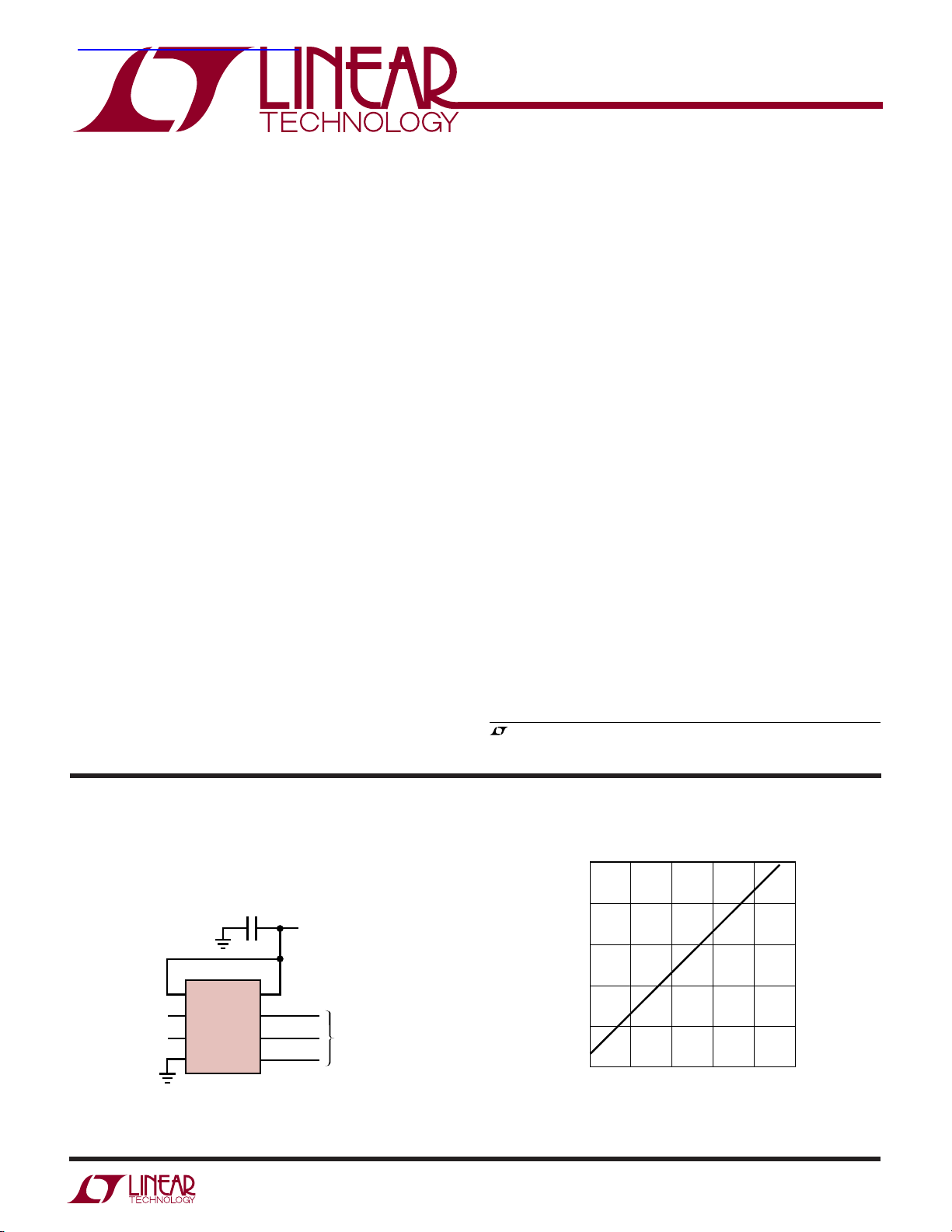
TYPICAL APPLICATIO
Single 5V Supply, 250ksps, 16-Bit Sampling ADC
1µF
LTC1864
ANALOG INPUT
0V TO 5V
1
V
REF
2
+
IN
3
–
IN
4
GND
V
SCK
SDO
CONV
8
CC
7
6
5
1864 TA01
U
5V
SERIAL DATA LINK TO
ASIC, PLD, MPU, DSP
OR SHIFT REGISTERS
Supply Current vs Sampling Frequency
1000
100
10
1
SUPPLY CURRENT (µA)
0.1
0.01
0.01
0.1
SAMPLING FREQUENCY (kHz)
10
1
100
1864 TA02
1000
sn18645 18645fs
1
Page 2
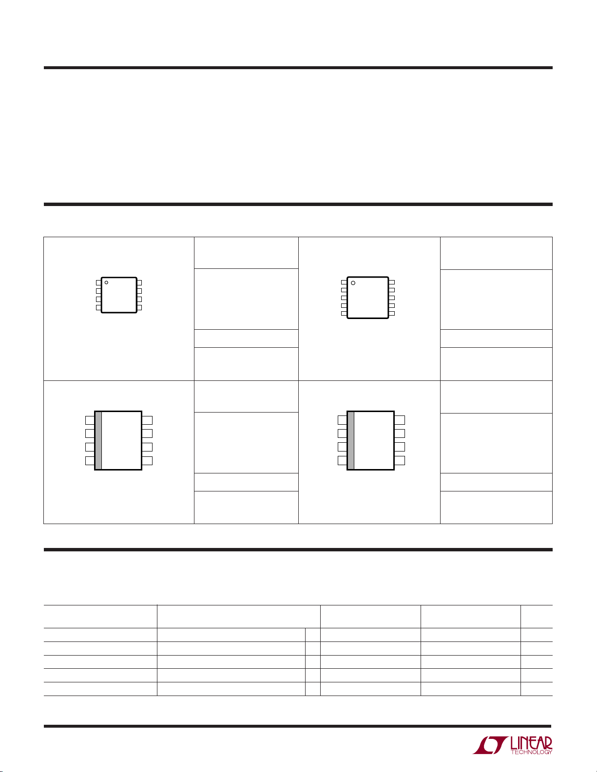
LTC1864/LTC1865
1
2
3
4
8
7
6
5
TOP VIEW
S8 PACKAGE
8-LEAD PLASTIC SO
CONV
CH0
CH1
GND
V
CC
SCK
SDO
SDI
1
2
3
4
5
CONV
CH0
CH1
AGND
DGND
10
9
8
7
6
V
REF
V
CC
SCK
SDO
SDI
TOP VIEW
MS PACKAGE
10-LEAD PLASTIC MSOP
WWWU
ABSOLUTE AXI U RATI GS
Supply Voltage (VCC) ................................................. 7V
Ground Voltage Difference
AGND, DGND LTC1865 MSOP Package ........... ±0.3V
Analog Input ............... (GND – 0.3V) to (V
Digital Input ................................ (GND – 0.3V) to 7V
Digital Output .............. (GND – 0.3V) to (V
Power Dissipation.............................................. 400mW
CC
CC
(Notes 1, 2)
+ 0.3V)
+ 0.3V)
Operating Temperature Range
LTC1864C/LTC1865C/
LTC1864AC/LTC1865AC ........................ 0°C to 70°C
LTC1864I/LTC1865I/
LTC1864AI/LTC1865AI ..................... –40°C to 85°C
Storage Temperature Range ................. – 65°C to 150°C
Lead Temperature (Soldering, 10 sec)................. 300°C
UU
W
PACKAGE/ORDER I FOR ATIO
ORDER PART
TOP VIEW
V
1
REF
+
2
IN
3
IN¯
4
GND
MS8 PACKAGE
8-LEAD PLASTIC MSOP
= 150°C, θJA = 210°C/W
T
JMAX
TOP VIEW
1
V
REF
+
2
IN
–
3
IN
4
GND
S8 PACKAGE
8-LEAD PLASTIC SO
T
= 150°C, θJA = 175°C/W
JMAX
Consult LTC Marketing for parts specified with wider operating temperature ranges.
8
7
6
5
8
7
6
5
V
CC
SCK
SDO
CONV
V
SCK
SDO
CONV
CC
NUMBER
LTC1864CMS8
LTC1864IMS8
LTC1864ACMS8
LTC1864AIMS8
MS8 PART MARKING
LTHQ
ORDER PART
NUMBER
LTC1864CS8
LTC1864IS8
LTC1864ACS8
LTC1864AIS8
S8 PART MARKING
1864
1864I
1864A
1864AI
T
= 150°C, θJA = 210°C/W
JMAX
T
= 150°C, θJA = 175°C/W
JMAX
ORDER PART
NUMBER
LTC1865CMS
LTC1865IMS
LTC1865ACMS
LTC1865AIMS
MS PART MARKING
LTHS
ORDER PART
NUMBER
LTC1865CS8
LTC1865IS8
LTC1865ACS8
LTC1865AIS8
S8 PART MARKING
1865
1865I
1865A
1865AI
W
U
U
CO VERTER A D ULTIPLEXER CHARACTERISTICS
The ● denotes specifications which apply over the full operating temperature range, otherwise specifications are TA = 25°C.
VCC = 5V, V
PARAMETER CONDITIONS MIN TYP MAX MIN TYP MAX UNITS
Resolution ● 16 16 Bits
No Missing Codes Resolution ● 14 15 Bits
INL (Note 3) ● ±8 ±6 LSB
Transition Noise 1.1 1.1 LSB
Gain Error ● ±20 ±20 mV
2
REF
= 5V, f
SCK
= f
SCK(MAX)
as defined in Recommended Operating Conditions, unless otherwise noted.
LTC1864/LTC1865 LTC1864A/LTC1865A
RMS
sn18645 18645fs
Page 3
LTC1864/LTC1865
W
U
U
CO VERTER A D ULTIPLEXER CHARACTERISTICS
The ● denotes specifications which apply over the full operating temperature range, otherwise specifications are TA = 25°C.
VCC = 5V, V
PARAMETER CONDITIONS MIN TYP MAX MIN TYP MAX UNITS
Offset Error LTC1864 SO-8 and MSOP, LTC1865 MSOP ● ±2 ±5 ±2 ±5mV
Input Differential Voltage Range VIN = IN+ – IN
Absolute Input Range IN+ Input –0.05 VCC + 0.05 –0.05 VCC + 0.05 V
V
Input Range LTC1864 SO-8 and MSOP, 1 V
REF
Analog Input Leakage Current (Note 4) ● ±1 ±1 µA
CIN Input Capacitance In Sample Mode 12 12 pF
U
REF
= 5V, f
W
SCK
= f
SCK(MAX)
as defined in Recommended Operating Conditions, unless otherwise noted.
LTC1864/LTC1865 LTC1864A/LTC1865A
LTC1865 SO-8 ● ±3 ±7 ±3 ±7mV
–
–
Input –0.05 VCC/2 – 0.05 VCC/2 V
IN
LTC1865 MSOP
During Conversion 5 5 pF
● 0V
REF
CC
0V
1VCCV
REF
V
DY A IC ACCURACY
TA = 25°C. VCC = 5V, V
SYMBOL PARAMETER CONDITIONS MIN TYP MAX UNITS
SNR Signal-to-Noise Ratio 87 dB
S/(N + D) Signal-to-Noise Plus Distortion Ratio 10kHz Input Signal 83 dB
THD Total Hamonic Distortion Up to 5th Harmonic 10kHz Input Signal 88 dB
Full Power Bandwidth 20 MHz
Full Linear Bandwidth S/(N + D) ≥ 75dB 125 kHz
REF
= 5V, f
= 250kHz, unless otherwise noted.
SAMPLE
100kHz Input Signal 76 dB
100kHz Input Signal 77 dB
LTC1864/LTC1865
U
DIGITAL A D DC ELECTRICAL CHARACTERISTICS
over the full operating temperature range, otherwise specifications are TA = 25°C. VCC = 5V, V
SYMBOL PARAMETER CONDITION MIN TYP MAX UNITS
V
IH
V
IL
I
IH
I
IL
V
OH
V
OL
I
OZ
I
SOURCE
I
SINK
I
REF
I
CC
P
D
High Level Input Voltage VCC = 5.25V ● 2.4 V
Low Level Input Voltage VCC = 4.75V ● 0.8 V
High Level Input Current VIN = V
Low Level Input Current VIN = 0V ● –2.5 µA
High Level Output Voltage VCC = 4.75V, IO = 10µA ● 4.5 4.74 V
Low Level Output Voltage VCC = 4.75V, IO = 1.6mA ● 0.4 V
Hi-Z Output Leakage CONV = V
Output Source Current V
Output Sink Current V
Reference Current (LTC1864 SO-8 and CONV = V
MSOP, LTC1865 MSOP) f
Supply Current CONV = V
Power Dissipation f
CC
= 4.75V, IO = 360µA ● 2.4 4.72 V
V
CC
CC
= 0V –25 mA
OUT
= V
OUT
CC
CC
= f
SMPL
SMPL(MAX)
After Conversion ● 0.001 3 µA
CC
= f
f
SMPL
SMPL(MAX)
= f
SMPL
SMPL(MAX)
The ● denotes specifications which apply
= 5V, unless otherwise noted.
REF
LTC1864/LTC1865
● 2.5 µA
● ±3 µA
20 mA
● 0.001 3 µA
● 0.05 0.1 mA
● 0.85 1.3 mA
4.25 mW
sn18645 18645fs
3
Page 4
LTC1864/LTC1865
UUUUWW
RECO E DED OPERATI G CO DITIO S
SCK(MAX)
SCK(MAX)
= 25°C.
A
full operating temperature range, otherwise specifications are T
SYMBOL PARAMETER CONDITIONS MIN TYP MAX UNITS
V
CC
f
SCK
t
CYC
t
SMPL
t
suCONV
t
hDI
t
suDI
t
WHCLK
t
WLCLK
t
WHCONV
t
WLCONV
t
hCONV
Supply Voltage 4.75 5.25 V
Clock Frequency ● DC 20 MHz
Total Cycle Time 16 • SCK + t
Analog Input Sampling Time LTC1864 16 SCK
LTC1865 14 SCK
Setup Time CONV↓ Before First SCK↑ 30 ns
(See Figure 1)
Hold Time SDI After SCK↑ LTC1865 15 ns
Setup Time SDI Stable Before SCK↑ LTC1865 15 ns
SCK High Time f
SCK Low Time f
CONV High Time Between Data t
Transfer Cycles
CONV Low Time During Data Transfer 16 SCK
Hold Time CONV Low After Last SCK↑ 13 ns
SCK
SCK
= f
= f
The ● denotes specifications which apply over the
LTC1864/LTC1865
CONV
40% 1/f
40% 1/f
CONV
µs
SCK
SCK
µs
UW
TI I G CHARACTERISTICS
range, otherwise specifications are TA = 25°C. VCC = 5V, V
Conditions, unless otherwise noted.
SYMBOL PARAMETER CONDITIONS MIN TYP MAX UNITS
t
CONV
f
SMPL(MAX)
t
dDO
t
dis
t
en
t
hDO
t
r
t
f
Note 1: Absolute Maximum Ratings are those values beyond which the life
of a device may be impaired.
Note 2: All voltage values are with respect to GND.
Conversion Time (See Figure 1) ● 2.75 3.2 µs
Maximum Sampling Frequency ● 250 kHz
Delay Time, SCK↓ to SDO Data Valid C
Delay Time, CONV↑ to SDO Hi-Z ● 30 60 ns
Delay Time, CONV↓ to SDO Enabled C
Time Output Data Remains C
Valid After SCK↓
SDO Rise Time C
SDO Fall Time C
The ● denotes specifications which apply over the full operating temperature
= 5V, f
REF
= 20pF 15 20 ns
LOAD
= 20pF ● 30 60 ns
LOAD
= 20pF ● 510 ns
LOAD
= 20pF 8 ns
LOAD
= 20pF 4 ns
LOAD
= f
SCK
SCK(MAX)
Note 3: Integral nonlinearity is defined as deviation of a code from a
straight line passing through the actual endpoints of the transfer curve.
The deviation is measured from the center of the quantization band.
Note 4: Channel leakage current is measured while the part is in sample
mode.
as defined in Recommended Operating
LTC1864/LTC1865
● 25 ns
4
sn18645 18645fs
Page 5

UW
V
REF
(V)
0
REFERENCE CURRENT (µA)
60
50
40
30
20
10
0
1234
1864/65 G06
5
V
CC
= 5V
T
A
= 25°C
f
S
= 250kHz
TEMPERATURE (°C)
–50
ANALOG INPUT LEAKAGE (nA)
100
1864/65 G09
050
100
75
50
25
0
–25 25 75 125
VCC = 5V
V
REF
= 5V
CONV = 0V
TYPICAL PERFOR A CE CHARACTERISTICS
Supply Current vs Sampling
1000
SUPPLY CURRENT (µA)
0.01
100
10
1
0.1
0.01
Frequency
VCC = 5V
= 25°C
T
A
CONV LOW = 800ns
0.1
1.0
SAMPLING FREQUENCY (kHz)
10
100
1000
1864/65 G01
Supply Current vs Temperature
1000
800
600
400
SUPPLY CURRENT (µA)
200
0
–50
0
–25
TEMPERATURE (°C)
VCC = 5V
V
REF
f
SAMPLE
CONV HIGH = 3.2µS
50
25
= 5V
= 250kHz
75
100
1864/65 G02
125
LTC1864/LTC1865
Sleep Current vs Temperature
1000
CONV = V
900
800
700
600
500
400
300
SLEEP CURRENT (nA)
200
100
0
–50
= 5V
CC
0
–25
TEMPERATURE (°C)
50
25
75
100
125
1864/65 G03
Reference Current vs
Sampling Rate
60
VCC = 5V
= 25°C
T
A
50
= 5V
V
REF
CONV LOW = 800ns
40
30
20
REFERENCE CURRENT (µA)
10
0
0
50 100 150 200
SAMPLE RATE (kHz)
Typical INL Curve
4
VCC = 5V
= 25°C
T
A
= 5V
V
REF
2
1864/65 G04
250
Reference Current vs
Temperature
55
V
= 5V
CC
54
= 5V
V
REF
= 250kHz
f
S
53
52
51
50
49
48
REFERENCE CURRENT (µA)
47
46
45
–50
0
–25
TEMPERATURE (°C)
Typical DNL Curve
2
VCC = 5V
= 25°C
T
A
= 5V
V
REF
1
Reference Current vs
Reference Voltage
50
25
75
100
1864/65 G05
125
Analog Input Leakage Current vs
Temperature
0
INL ERROR (LSBs)
–2
–4
0
0
DNL ERROR (LSBs)
–1
16384
32768
CODE
49152
65536
1864/65 G07
–2
0 65536
3276816384
CODE
49152
1864/65 G08
sn18645 18645fs
5
Page 6

LTC1864/LTC1865
UW
TYPICAL PERFOR A CE CHARACTERISTICS
Change in Offset Error vs
Reference Voltage
75
50
25
0
CHANGE IN OFFSET ERROR (LSB)
–25
1
0
2
REFERENCE VOLTAGE (V)
Change in Gain Error vs
Temperature
5
VCC = 5V
4
= 5V
V
REF
3
2
1
0
–1
–2
–3
CHANGE IN GAIN ERROR (LSB)
–4
–5
–50
–25
25
0
TEMPERATURE (°C)
Change in Gain Error vs
Change in Offset vs Temperature
5
VCC = 5V
= 25°C
T
A
3
4
5
1864/65 G10
VCC = 5V
4
= 5V
V
REF
3
2
1
0
–1
–2
CHANGE IN OFFSET (LSB)
–3
–4
–5
–50
–25
0
TEMPERATURE (°C)
50
25
75
100
1864/65 G11
125
Reference Voltage
20
VCC = 5V
= 25°C
T
15
A
10
5
0
–5
–10
CHANGE IN GAIN ERROR (LSB)
–15
–20
0
2
1
REFERENCE VOLTAGE(V)
4
3
5
1864/65 G12
Histogram of 4096 Conversions
of a DC Input Voltage
1800
127
729
1534
0
1178
1
CODE
1600
1400
1200
1000
800
FREQUENCY
600
400
200
00 1200
50
75
100
1864/65 G13
125
0
–4 –3 –2 –1
VCC = 5V
= 25°C
T
A
= 5V
V
REF
516
2345
1864/65 G14
4096 Point FFT Nonaveraged
0
fS = 203.125kHz
= 99.72763kHz
f
IN
–20
= 5V
V
CC
= 5V
V
REF
–40
= 25°C
T
A
–60
–80
AMPLITUDE (dB)
–100
–120
–140
0
40 60 80 100 120
20
FREQUENCY (kHz)
1864/65 G15
SINAD vs Frequency
100
90
80
70
60
50
SINAD (dB)
40
30
20
10
0
1
6
SNR
SINAD
VCC = 5V
= 5V
V
REF
= 25°C
T
A
= 0dB
V
IN
10 100 1000
FIN (kHz)
1864/5 G16
THD vs Frequency
0
–10
–20
–30
–40
–50
THD (dB)
–60
–70
–80
–90
–100
1
VCC = 5V
= 5V
V
REF
= 25°C
T
A
= 0dB
V
IN
10 100 1000
FIN (kHz)
1864/5 G17
SFDR vs Frequency
100
90
80
70
60
50
SFDR (dB)
40
30
20
10
0
1
VCC = 5V
= 5V
V
REF
= 25°C
T
A
= 0dB
V
IN
10 100 1000
FIN (kHz)
1864/5 G18
sn18645 18645fs
Page 7

LTC1864/LTC1865
U
UU
PI FU CTIO S
LTC1864
V
(Pin 1): Reference Input. The reference input defines
REF
the span of the A/D converter and must be kept free of
noise with respect to GND.
IN+, IN– (Pins 2, 3): Analog Inputs. These inputs must be
free of noise with respect to GND.
GND (Pin 4): Analog Ground. GND should be tied directly
to an analog ground plane.
CONV (Pin 5): Convert Input. A logic high on this input
starts the A/D conversion process. If the CONV input is left
high after the A/D conversion is finished, the part powers
LTC1865 (MSOP Package)
CONV (Pin 1): Convert Input. A logic high on this input
starts the A/D conversion process. If the CONV input is left
high after the A/D conversion is finished, the part powers
down. A logic low on this input enables the SDO pin,
allowing the data to be shifted out.
CH0, CH1 (Pins 2, 3): Analog Inputs. These inputs must
be free of noise with respect to AGND.
AGND (Pin 4): Analog Ground. AGND should be tied
directly to an analog ground plane.
DGND (Pin 5): Digital Ground. DGND should be tied
directly to an analog ground plane.
down. A logic low on this input enables the SDO pin,
allowing the data to be shifted out.
SDO (Pin 6): Digital Data Output. The A/D conversion
result is shifted out of this pin.
SCK (Pin 7): Shift Clock Input. This clock synchronizes the
serial data transfer.
V
(Pin 8):
CC
free of noise and ripple by bypassing directly to the
analog ground plane.
SDO (Pin 7): Digital Data Output. The A/D conversion
result is shifted out of this output.
SCK (Pin 8): Shift Clock Input. This clock synchronizes the
serial data transfer.
VCC (Pin 9):
free of noise and ripple by bypassing directly to the
analog ground plane.
V
(Pin 10): Reference Input. The reference input de-
REF
fines the span of the A/D converter and must be kept free
of noise with respect to AGND.
Positive Supply. This supply must be kept
Positive Supply. This supply must be kept
SDI (Pin 6):
word is shifted into this input.
LTC1865 (SO-8 Package)
CONV (Pin 1): Convert Input. A logic high on this input
starts the A/D conversion process. If the CONV input is left
high after the A/D conversion is finished, the part powers
down. A logic low on this input enables the SDO pin,
allowing the data to be shifted out.
CH0, CH1 (Pins 2, 3): Analog Inputs. These inputs must
be free of noise with respect to GND.
GND (Pin 4): Analog Ground. GND should be tied directly
to an analog ground plane.
Digital Data Input. The A/D configuration
SDI (Pin 5):
word is shifted into this input.
SDO (Pin 6): Digital Data Output. The A/D conversion
result is shifted out of this output.
SCK (Pin 7): Shift Clock Input. This clock synchronizes the
serial data transfer.
VCC (Pin 8):
free of noise and ripple by bypassing directly to the
analog ground plane. V
Digital Data Input. The A/D configuration
Positive Supply. This supply must be kept
is tied internally to this pin.
REF
sn18645 18645fs
7
Page 8

LTC1864/LTC1865
SDO
WAVEFORM 1
(SEE NOTE 1)
V
IH
t
dis
90%
10%
SDO
WAVEFORM 2
(SEE NOTE 2)
CONV
NOTE 1: WAVEFORM 1 IS FOR AN OUTPUT WITH INTERNAL CONDITIONS SUCH
THAT THE OUTPUT IS HIGH UNLESS DISABLED BY THE OUTPUT CONTROL
NOTE 2: WAVEFORM 2 IS FOR AN OUTPUT WITH INTERNAL CONDITIONS SUCH
THAT THE OUTPUT IS LOW UNLESS DISABLED BY THE OUTPUT CONTROL
1864 TC05
UU
W
FUNCTIONAL BLOCK DIAGRA
PIN NAMES IN
PARENTHESES
IN
(CH0)
IN
(CH1)
+
–
REFER TO LTC1865
GND
CONVERT
CLK
+
–
V
CC
BIAS AND
SHUTDOWN
16-BIT
SAMPLING
ADC
V
REF
DATA IN
DATA OUT
CONV
(SDI) SCK
SERIAL
PORT
16 BITS
SDO
1864/65 BD
TEST CIRCUITS
Load Circuit for t
TEST POINT
SDO
3k
20pF
Voltage Waveforms for t
CONV
SDO
Voltage Waveforms for SDO Delay Times, t
8
SCK
SDO
t
V
hDO
IL
t
dDO
dDO
, tr, tf, t
t
en
VCC t
t
dis
and t
dis
WAVEFORM 2, t
dis
WAVEFORM 1
en
dDO
en
1864 TC03
and t
1864 TC02
1864 TC01
Voltage Waveforms for SDO Rise and Fall Times, tr, t
SDO
en
t
r
Voltage Waveforms for t
dis
t
f
1864 TC04
f
V
OH
V
OL
hDO
V
OH
V
OL
sn18645 18645fs
Page 9

WUUU
APPLICATIO S I FOR ATIO
LTC1864/LTC1865
LTC1864 OPERATION
Operating Sequence
The LTC1864 conversion cycle begins with the rising edge
of CONV. After a period equal to t
, the conversion is
CONV
finished. If CONV is left high after this time, the LTC1864
goes into sleep mode drawing only leakage current. On the
falling edge of CONV, the LTC1864 goes into sample mode
and SDO is enabled. SCK synchronizes the data transfer
with each bit being transmitted from SDO on the falling
SCK edge. The receiving system should capture the data
from SDO on the rising edge of SCK. After completing the
data transfer, if further SCK clocks are applied with CONV
low, SDO will output zeros indefinitely. See Figure 1.
CONV
SCK
t
CONV
SLEEP MODE
Analog Inputs
The LTC1864 has a unipolar differential analog input. The
converter will measure the voltage between the “IN+” and
“IN–” inputs. A zero code will occur when IN+ minus IN
–
equals zero. Full scale occurs when IN+ minus IN– equals
V
minus 1LSB. See Figure 2. Both the “IN+” and
REF
“IN–” inputs are sampled at the same time, so common
–
mode noise on the inputs is rejected by the ADC. If “IN
is grounded and V
is tied to VCC, a rail-to-rail input span
REF
”
will result on “IN+” as shown in Figure 3.
Reference Input
The voltage on the reference input of the LTC1864 defines
the full-scale range of the A/D converter. The LTC1864 can
operate with reference voltages from VCC to 1V.
t
SMPL
16151413121110987654321
SDO
1 1 1 1 1 1 1 1 1 1 1 1 1 1 1 1
1 1 1 1 1 1 1 1 1 1 1 1 1 1 1 0
•
•
•
0 0 0 0 0 0 0 0 0 0 0 0 0 0 0 1
0 0 0 0 0 0 0 0 0 0 0 0 0 0 0 0
Hi-Z
B14 B12 B10 B8 B6 B4 B2 B0*
B15
*AFTER COMPLETING THE DATA TRANSFER, IF FURTHER SCK CLOCKS ARE
APPLIED WITH CONV LOW, THE ADC WILL OUTPUT ZEROS INDEFINITELY
B11 B9 B7 B5 B3 B 1
B13
Hi-Z
1854 F01
Figure 1. LTC1864 Operating Sequence
1µF
V
CC
LTC1864
1
V
REF
2
VIN = 0V TO V
VIN*
0V
1LSB
*V
IN
= IN+ – IN
V
REF
–
– 2LSB
V
REF
– 1LSB
V
REF
1864 F02
CC
+
IN
3
–
IN
4
GND
V
SCK
SDO
CONV
8
CC
7
6
5
1864 F03
SERIAL DATA LINK TO
ASIC, PLD, MPU, DSP
OR SHIFT REGISTERS
Figure 3. LTC1864 with Rail-to-Rail Input SpanFigure 2. LTC1864 Transfer Curve
sn18645 18645fs
9
Page 10

LTC1864/LTC1865
MUX ADDRESS
Table 1. Multiplexer Channel Selection
SGL/DIFF
1
1
0
0
ODD/SIGN
0
1
0
1
CHANNEL #
0
+
+
–
1
+
–
+
GND
–
–
1864 TBL1
SINGLE-ENDED
MUX MODE
DIFFERENTIAL
MUX MODE
WUUU
APPLICATIO S I FOR ATIO
LTC1865 OPERATION
Operating Sequence
The LTC1865 conversion cycle begins with the rising edge
of CONV. After a period equal to t
, the conversion is
CONV
finished. If CONV is left high after this time, the LTC1865
goes into sleep mode drawing only leakage current. The
LTC1865’s 2-bit data word is clocked into the SDI input on
the rising edge of SCK after CONV goes low. Additional
inputs on the SDI pin are then ignored until the next CONV
cycle. The shift clock (SCK) synchronizes the data transfer
with each bit being transmitted on the falling SCK edge and
captured on the rising SCK edge in both transmitting and
receiving systems. The data is transmitted and received
simultaneously (full duplex). After completing the data
transfer, if further SCK clocks are applied with CONV low,
SDO will output zeros indefinitely. See Figure 4.
Analog Inputs
The two bits of the input word (SDI) assign the MUX
configuration for the next requested conversion. For a
given channel selection, the converter will measure the
voltage between the two channels indicated by the “+”
and “–” signs in the selected row of the following table. In
single-ended mode, all input channels are measured with
respect to GND. A zero code will occur when the “+” input
minus the “–” input equals zero. Full scale occurs when
the “+” input minus the “–” input equals V
REF
minus
1LSB. See Figure 5. Both the “+” and “–” inputs are
sampled at the same time so common mode noise is
rejected. The input span in the SO-8 package is fixed at
V
= VCC. If the “–” input in differential mode is
REF
grounded, a rail-to-rail input span will result on the “+”
input.
Reference Input
The reference input of the LTC1865 SO-8 package is
internally tied to VCC. The span of the A/D converter is
therefore equal to VCC. The voltage on the reference input
of the LTC1865 MSOP package defines the span of the
A/D converter. The LTC1865 MSOP package can operate
with reference voltages from 1V to VCC.
CONV
SDI
SCK
SDO
10
t
CONV
Hi-Z
SLEEP MODE
S/D O/S
B14 B12 B10 B8 B6 B 4 B 2
B15
*AFTER COMPLETING THE DATA TRANSFER, IF FURTHER SCK CLOCKS ARE
APPLIED WITH CONV LOW, THE ADC WILL OUTPUT ZEROS INDEFINITELY
Figure 4. LTC1865 Operating Sequence
t
SMPL
DON’T CAREDON’T CARE
B11 B9 B7 B5 B3 B 1
B13
16151413121110987654321
B0*
Hi-Z
1864 F04
sn18645 18645fs
Page 11

WUUU
APPLICATIO S I FOR ATIO
LTC1864/LTC1865
GENERAL ANALOG CONSIDERATIONS
Grounding
The LTC1864/LTC1865 should be used with an analog
ground plane and single point grounding techniques. Do
not use wire wrapping techniques to breadboard and
evaluate the device. To achieve the optimum performance,
use a printed circuit board. The ground pins (AGND and
DGND for the LTC1865 MSOP package and GND for the
LTC1864 and LTC1865 SO-8 package) should be tied
directly to the analog ground plane with minimum lead
length.
Bypassing
For good performance, the VCC and V
of noise and ripple. Any changes in the VCC/V
pins must be free
REF
voltage
REF
with respect to ground during the conversion cycle can
induce errors or noise in the output code. Bypass the V
and V
pins directly to the analog ground plane with a
REF
CC
minimum of 1µF tantalum. Keep the bypass capacitor
leads as short as possible.
Analog Inputs
Because of the capacitive redistribution A/D conversion
techniques used, the analog inputs of the LTC1864/
LTC1865 have capacitive switching input current spikes.
These current spikes settle quickly and do not cause a
problem if source resistances are less than 200Ω or high
speed op amps are used (e.g., the LT
®
1211, LT1469,
LT1807, LT1810, LT1630, LT1226 or LT1215). But if large
source resistances are used, or if slow settling op amps
drive the inputs, take care to ensure the transients caused
by the current spikes settle completely before the conversion begins.
1 1 1 1 1 1 1 1 1 1 1 1 1 1 1 1
1 1 1 1 1 1 1 1 1 1 1 1 1 1 1 0
•
•
•
0 0 0 0 0 0 0 0 0 0 0 0 0 0 0 1
0 0 0 0 0 0 0 0 0 0 0 0 0 0 0 0
0V
1LSB
*V
= (SELECTED “+” CHANNEL) –
IN
(SELECTED “–” CHANNEL)
REFER TO TABLE 1
Figure 5. LTC1865 Transfer Curve
V
CC
– 2LSB
V
CC
– 1LSB
V
CC
1864 F05
*
V
IN
sn18645 18645fs
11
Page 12

LTC1864/LTC1865
WUUU
APPLICATIO S I FOR ATIO
40383634323028262422201816141210864
J4
3201S40G1
393735333129272523211917151311
C14
0.1µF
DIG
5V
C13
0.1µF
DIG
5V
C26
DIG
5V
R4
2Ω
AN
5V
3
OUT
V
IN
V
1
15V
LTC1864 Evaluation Circuit Schematic
C2
10µF
GND
1µF
C1
6.3V
2
5V
10V
0.1µF
1234567
QB
QC
CC
QAAOENB
V
U4
74HC595ADT
16151413121110
DIG
5V
1206
C4
0.1µF
AN
C3
6.3V
10µF
0805
QD
1206
RN1
QE
330
876
123
QF
QG
LCLK
SCLK
876
123
CC
V
SCK
REF
V
IN+IN–GND
R5
C8
8
QH
RESET
9
402Ω, 1%
5
SDO
4
1000pF
C7
GND
SQH
U8A
C21
5
4
CONV
OPT
390pF
1234567
QB
QC
CC
QAAOENB
V
16151413121110
74AC14
R6
47pF
U3
LTC1864CMS8
C10
680pF
OPT
C9
180pF
2
97531
QF
QE
QD
QG
QH
LCLK
SCLK
RESET
U8B
74AC14
1%
C22
402Ω
47pF
ANALOG GROUND PLANE
C12
1000pF
OPT
C11
390pF
CONV
DGND
DGND
DOUT
CLKOUT
ENABLE
C25
DATA
E2
E3
E7
E6
E4
2
1
JP5
U8F
74AC14
U8E
74AC14
0.1µF
DIG
5V
8
CLR
8
CLR
GND
PRE
GND
PRE
U8D
74AC14
C17
0.1µF
DIG
5V
C16
0.1µF
DIG
5V
DIG
5V
C15
0.1µF
DIG
5V
U9D
74AC00
8
U9C
0.1µF
DIG
0.1µF
DIG
U5
74HC595ADT
16
U12B
74AC109
16
U12A
74AC109
74AC00
21
JP4
10
9
Q
Q
CC
V
JKCLK
1413121511
6
7
Q
Q
CC
V
JKCLK
23415
GND
SQH
9
C24
5V
C23
5V
CLKIN
J3
E5
C18
0.1µF
DIG
5V
10k
R12
16151413121110
CC
V
RESET
U7
74HC163AD
1234567
R9
51Ω
C19
0.1µF
DIG
5V
JP7
2
1
JP6
5
OUT
V+GND
U10
LTC1799
123
Q0Q1Q2
RCO
CLKP0P1P2P3
U13D
U13A
3
21
3
4
DIV
SET
R10
Q3
ENT
ENP
74AC32
74AC32
U8C
20k
9
LO
GND
8
74AC14
1864/65 AI1
NOTES: UNLESS OTHERWISE SPECIFIED
INSTALL SHUNTS ON JP1, JP3-JP7 PIN 1 AND PIN2;
ON JP8 AND JP9 PIN 2 AND PIN 4, PIN 3 AND PIN 5.
U13C
74AC32
CLK
U13B
74AC32
12
R2
510Ω
2
1
JP3
U9B
C6
0.1µF
–15V
–
IN
R8
51Ω
0PT
E9
J2
–
IN
74AC00
U9A
74AC00
DIG
5V
DIG
5V
16151413121110
CC
V
RCO
RESET
CLKP0P1P2P3
U6
74HC163AD
1234567
JP8
246
Q0Q1Q2
135
Q3
ENT
ENP
246
9
LO
GND
8
JP9
135
JP1
C5
R1
510Ω
21
JP2
0.1µF
U2
0PT
OPT
+
–
E8
AGND
15V
R7
51Ω
R3
2Ω
21
U1
LT1021-5
6
OUT
V
4
GND
IN
V
2
C27
0.1µF
+
IN
15V
J1
E1
15V
+
IN
sn18645 18645fs
Page 13

WUUU
APPLICATIO S I FOR ATIO
Component Side Silk Screen for LTC1864 Evaluation Circuit
LTC1864/LTC1865
Component Side Showing Traces
(Note Wider Traces on Analog Side)
Ground Layer with Separate Analog and Digital Grounds Supply Layer with 5V Digital Supply and Analog Ground Repeated
(Note Almost No Analog Traces on Board Bottom)
Bottom Side Showing Traces
sn18645 18645fs
13
Page 14

LTC1864/LTC1865
WUUU
APPLICATIO S I FOR ATIO
5V
DIG
U9B
74AC00
U9A
74AC00
U6
74HC163AD
1
RESET
2
CLK
3
P0
4
P1
5
P2
6
P3
7
ENP
8
GND
V
RCO
ENT
U11
15V
LT1121CST-5
1
VINV
GND
5V
AN
1V to 5V REFERENCE
0V to V
INPUT
REF
10µF
6.3V
1206
C3
0.1µF
1
V
REF
2
+
IN
3
–
IN
4
GND
U3
LTC1864CMS8
C4
RN1
330
8
V
SCK
SDO
CONV
CC
1
7
6
5
8
2
7
3
6
4
5
ANALOG GROUND PLANE
V
CC
J
K
v
CLK
CLR
PRE
DIG
C16
0.1µF
U7
74HC163AD
RESET
CLK
P0
P1
P2
P3
ENP
GND
U13B
74AC32
16
C23
0.1µF
GND
V
RCO
Q0
Q1
Q2
Q3
ENT
LO
5V
DIG
U12B
CLK
74AC109
14
13
12
15
11
5V
DIG
6
Q
7
Q
8
5V
DIG
C17
0.1µF
16
CC
15
14
13
100k
12
11
10
9
5V
DIG
U12A
74AC109
2
3
4
1
5
5V
5V
DIG
16
CC
15
14
Q0
13
Q1
12
Q2
11
Q3
10
9
LO
1
2
3
4
5
6
7
8
J
K
v
CLK
CLR
PRE
U10
LTC1799
1
V
2
GND
3
SET
C24
0.1µF
16
10
V
CC
Q
9
Q
8
GND
C18
0.1µF
OUT
DIV
5
4
+
1
5V
5
MC74VHC1G66
U13C
74AC32
4
5V
AN
3
OUT
2
2
500Ω
3
5V
DIG
R4
2Ω
5V
DIG
1
2
3
4
LTC1485
RO
RE
DE
DI
PRE
D
v
CLK
CLR
PRE
D
v
CLK
CLR
C26
10µF
6.3V
1206
5V
15V
DIG
8
V
CC
7
B
6
A
5
GND
5V
DIG
74AC74
5V
DIG
74AC74
120Ω
4 CONDUCTOR
TELEPHONE WIRES
TO RECEIVER
74AC86
Q
Q
Q
Q
1864/65 AI2
14
Figure 6. LTC1864 Manchester Transmitter
sn18645 18645fs
Page 15

WUUU
APPLICATIO S I FOR ATIO
LTC1864/LTC1865
V
CC
DATA IN
CLK
RECEIVE CLOCK AT
CLOCK FREQUENCY
IC1A
74AC74
4
PRE
2
D
3
v
CLK
1
CLR
8 X TRANSMIT
4 CONDUCTOR
TELEPHONE WIRES
TO TRANSMITTER
Q
Q
V
CC
5
6
CLK
15V SUPPLY TO
10
PRE
12
D
11
v
CLK
13
CLR
IC1B
74AC74
U1
LTC1485
1
RO
2
RE
3
DE
4
DI
TRANSMITTER
V
GND
R1
120Ω
V
CC
IC3A
74AC74
4
PRE
2
D
CLK
3
v
CLK
1
CLR
V
IC3B
CC
74AC74
10
PRE
12
D
CLK
11
v
CLK
13
CLR
IC8
74AC595
14
SER
11
SCK
10
SCL
V
CC
12
v
RCK
13
8
V
CC
IC9
74AC595
14
SER
11
SCK
10
SCL
10
9
12
v
RCK
13
8
5
Q
6
Q
9
Q
STROBE
8
Q
15
QA
D15
1
QB
D14
2
QC
D13
3
QD
D12
4
QE
D11
5
QF
D10
6
QG
D9
7
QH
D8
9
QH
IN
15
QA
D7
1
QB
D6
2
QC
D5
3
QD
D4
4
QE
D3
5
QF
D2
6
QG
D1
7
QH
D0
9
QH
IN
5
6
CLK
STROBE
DATA
V
CC
IC2B
74AC74
10
PRE
12
D
11
v
CLK
13
CLR
IC6C
74LS32D
IC4D
74AC08
OPTIONAL SERIAL TO
PARALLEL CONVERTER
11
14
12
13
15
9
Q
8
Q
IC4C
74AC08
IC7B
74AC109
PRE
J
v
CLK
K
CLR
IC4B
74AC08
Q
Q
V
CC
CLK
4
2
3
1
IC2A
74AC74
PRE
D
v
CLK
CLR
Q
Q
IC5C
74AC86
9
Q
8
DATA
Q
DATA
V
CC
8
CC
7
B
6
A
5
IC6D
74AC32
IC4A
74AC08
Figure 7. LTC1864 Manchester Receiver
1864/65 AI3
sn18645 18645fs
15
Page 16

LTC1864/LTC1865
WUUU
APPLICATIO S I FOR ATIO
Transmit LTC1864 Data Over Modular Telephone Wire
Using Simple Transmitter/Receiver
Figure 6 shows a simple Manchester encoder and differential transmitter suitable for use with the LTC1864. This
circuit allows transmission of data over inexpensive telephone wire. This is useful for measuring a remote sensor,
particularly when the cost of preserving the analog signal
over a long distance is high.
Manchester encoding is a clock signal that is modulated
by exclusive ORing with the data signal. The resulting
signal contains both clock and data information and has an
average duty cycle of 50%, that also allows transformer
coupling. In practice, generating a Manchester encoded
signal with an XOR gate will often produce glitches due to
the skew between data and clock transitions. The D flipflops in this encoder retime the clock and data such that
the respective edges are closely aligned, effectively suppressing glitches. The retimed data and clock are then
XORed to produce the Manchester encoded data, which is
interfaced to telephone wire with an LTC1485 RS485
transceiver.
In order to synchronize to incoming data, the receiver
needs a sequence to indicate the start of a data word. The
transmitter schematic shows logic that will produce 31
zeros, a start bit, followed by the 16 data bits (one sample
every 48 clock cycles) at a clock frequency of 1MHz set by
the LTC1799 oscillator. Sending at least 18 zeros before
each start bit ensures that if synchronization is lost, the
receiver can resynchronize to a start bit under all conditions. The serial to parallel converter shown in Figure 7
requires 18 zeros to avoid triggering on data bits.
The Manchester receiver shown in Figure 7 was adopted
from Xilinx application note 17-30 and would typically be
implemented in an FPGA. The decoder clock frequency is
nominally 8 times the transmit clock frequency and is very
tolerant of frequency errors. The outputs of the decoder
are data and a strobe that indicates a valid data bit. The data
can be deserialized using shift registers as shown. The
start bit resets the J-K/flip-flop on its way into the first shift
register. When it appears at the QH
shift register, it sets the flip-flop that loads the parallel data
into the output register.
With AC family CMOS logic at 5V the receiver clock
frequency is limited to 20MHz; the corresponding transmitter clock frequency is 2.5MHz. If the receiver is implemented in an FPGA that can be clocked at 160MHz, the
LTC1864 can be clocked at its rated clock frequency of
20MHz.
output of the second
IN
16
sn18645 18645fs
Page 17

PACKAGE DESCRIPTIO
LTC1864/LTC1865
U
MS8 Package
8-Lead Plastic MSOP
(Reference LTC DWG # 05-08-1660)
5.23
(.206)
MIN
0.42 ± 0.04
(.0165 ± .0015)
TYP
RECOMMENDED SOLDER PAD LAYOUT
PLANE
3.00 ± 0.102
(.118 ± .004)
(NOTE 3)
4.88
± 0.1
(.192 ± .004)
0.22 – 0.38
(.009 – .015)
1.10
(.043)
MAX
0.889 ± 0.127
(.035 ± .005)
3.2 – 3.45
(.126 – .136)
0.65
(.0256)
BSC
NOTE:
1. DIMENSIONS IN MILLIMETER/(INCH)
2. DRAWING NOT TO SCALE
3. DIMENSION DOES NOT INCLUDE MOLD FLASH, PROTRUSIONS OR GATE BURRS.
MOLD FLASH, PROTRUSIONS OR GATE BURRS SHALL NOT EXCEED 0.152mm (.006") PER SIDE
4. DIMENSION DOES NOT INCLUDE INTERLEAD FLASH OR PROTRUSIONS.
INTERLEAD FLASH OR PROTRUSIONS SHALL NOT EXCEED 0.152mm (.006") PER SIDE
5. LEAD COPLANARITY (BOTTOM OF LEADS AFTER FORMING) SHALL BE 0.102mm (.004") MAX
GAUGE PLANE
0.18
(.077)
0.254
(.010)
DETAIL “A”
DETAIL “A”
° – 6° TYP
0
0.53 ± 0.015
(.021 ± .006)
SEATING
8
12
0.65
(.0256)
BCS
0.52
5
4
(.206)
REF
3.00 ± 0.102
(.118 ± .004)
NOTE 4
0.86
(.034)
REF
0.13 ± 0.05
(.005 ± .002)
MSOP (MS8) 1001
7
6
3
sn18645 18645fs
17
Page 18

LTC1864/LTC1865
PACKAGE DESCRIPTIO
0.889 ± 0.127
(.035 ± .005)
U
MS Package
10-Lead Plastic MSOP
(Reference LTC DWG # 05-08-1661)
3.00 ± 0.102
(.118 ± .004)
(NOTE 3)
0.497 ± 0.076
8910
(.0196 ± .003)
7
6
REF
5.23
(.206)
MIN
0.305 ± 0.038
(.0120 ± .0015)
TYP
RECOMMENDED SOLDER PAD LAYOUT
NOTE:
1. DIMENSIONS IN MILLIMETER/(INCH)
2. DRAWING NOT TO SCALE
3. DIMENSION DOES NOT INCLUDE MOLD FLASH, PROTRUSIONS OR GATE BURRS.
MOLD FLASH, PROTRUSIONS OR GATE BURRS SHALL NOT EXCEED 0.152mm (.006") PER SIDE
4. DIMENSION DOES NOT INCLUDE INTERLEAD FLASH OR PROTRUSIONS.
INTERLEAD FLASH OR PROTRUSIONS SHALL NOT EXCEED 0.152mm (.006") PER SIDE
5. LEAD COPLANARITY (BOTTOM OF LEADS AFTER FORMING) SHALL BE 0.102mm (.004") MAX
3.2 – 3.45
(.126 – .136)
0.50
(.0197)
BSC
GAUGE PLANE
0.18
(.007)
0.254
(.010)
DETAIL “A”
DETAIL “A”
0° – 6° TYP
0.53 ± 0.01
(.021 ± .006)
SEATING
PLANE
4.88 ± 0.10
(.192 ± .004)
(.043)
0.17 – 0.27
(.007 – .011)
1.10
MAX
12
0.50
(.0197)
TYP
3
3.00 ± 0.102
(.118 ± .004)
NOTE 4
45
0.86
(.034)
REF
0.13 ± 0.05
(.005 ± .002)
MSOP (MS) 1001
18
sn18645 18645fs
Page 19

PACKAGE DESCRIPTIO
U
S8 Package
8-Lead Plastic Small Outline (Narrow .150 Inch)
(Reference LTC DWG # 05-08-1610)
0.189 – 0.197*
(4.801 – 5.004)
7
8
6
LTC1864/LTC1865
5
0.228 – 0.244
(5.791 – 6.197)
0.010 – 0.020
(0.254 – 0.508)
0.008 – 0.010
(0.203 – 0.254)
*
DIMENSION DOES NOT INCLUDE MOLD FLASH. MOLD FLASH
SHALL NOT EXCEED 0.006" (0.152mm) PER SIDE
**
DIMENSION DOES NOT INCLUDE INTERLEAD FLASH. INTERLEAD
FLASH SHALL NOT EXCEED 0.010" (0.254mm) PER SIDE
×
°
45
0.016 – 0.050
(0.406 – 1.270)
0°– 8° TYP
0.053 – 0.069
(1.346 – 1.752)
0.014 – 0.019
(0.355 – 0.483)
TYP
0.150 – 0.157**
(3.810 – 3.988)
SO8 1298
1
3
2
4
0.004 – 0.010
(0.101 – 0.254)
0.050
(1.270)
BSC
Information furnished by Linear Technology Corporation is believed to be accurate and reliable.
However, no responsibility is assumed for its use. Linear Technology Corporation makes no representation that the interconnection of its circuits as described herein will not infringe on existing patent rights.
sn18645 18645fs
19
Page 20

LTC1864/LTC1865
TYPICAL APPLICATIO
Sample Two Channels Simultaneously with a Single Input ADC
0.1µF
f
(0V TO 0.66V)
4.096V
REF
28.7k
10k
(0V TO 2V)
1
1µF
0.1µF
f
2
+
1/2
LT1492
–
5k
10k
5k
+
LT1492
–
1/2
20k
5pF
5V
0.1µF
8
4
U
100Ω
100pF
100Ω
100pF
4096 Point FFT of Output
5V
4.096V
REF
81
V
CC
2
+
IN
–
IN
3
LTC1864
GND
REF
SCK
SDO
CONV
4
0.1µF1µF
0.1µF
7
6
5
1µF
1860 TA03
0
10
20
30
40
50
60
70
80
AMPLITUDE (dB)
90
100
110
120
130
f1 = 7.507324kHz AT 530mV
f2 = 45.007324kHz AT 1.7V
fS = 100kHz
0 5 10 15 20 25 30 35 40 45 50
FREQUENCY (kHz)
P-P
P-P
1864/65 TA03b
RELATED PARTS
PART NUMBER SAMPLE RATE POWER DISSIPATION DESCRIPTION
14-Bit Serial I/O ADCs
LTC1417 400ksps 20mW 16-Pin SSOP, Unipolar or Bipolar, Reference, 5V or ±5V
LTC1418 200ksps 15mW Serial/Parallel I/O, Internal Reference, 5V or ±5V
16-Bit Serial I/O ADCs
LTC1609 200ksps 65mW Configurable Bipolar or Unipolar Input Ranges, 5V
References
LT1460 Micropower Precision Series Reference Bandgap, 130µA Supply Current, 10ppm/°C, Available in SOT-23
LT1790 Micropower Low Dropout Reference 60µA Supply Current, 10ppm/°C, SOT-23
Op Amps
LT1468/LT1469 Single/Dual 90MHz, 16-Bit Accurate Op Amps 22V/µs Slew Rate, 75µV/125µV Offset
LT1806/LT1807 Single/Dual 325MHz Low Noise Op Amps 140V/µs Slew Rate, 3.5nV/√Hz Noise, – 80dBc Distortion
LT1809/LT1810 Single/Dual 180MHz Low Distortion Op Amps 350V/µs Slew Rate, –90dBc Distortion at 5MHz
20
Linear Technology Corporation
1630 McCarthy Blvd., Milpitas, CA 95035-7417
(408) 432-1900 ● FAX: (408) 434-0507
●
www.linear.com
sn18645 18645fs
LT/TP 0502 2K • PRINTED IN USA
© LINEAR TECHNOLOGY CORPORATION 2001
 Loading...