

Page 1
FEATURES
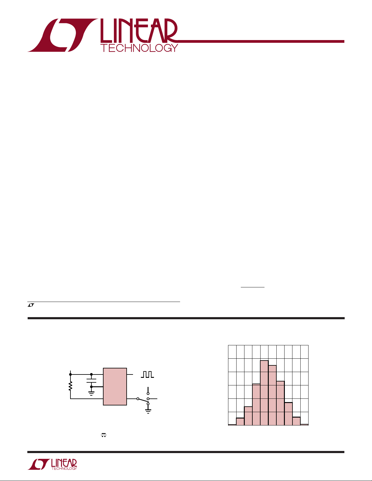
UNITS (%)
25
20
15
10
5
0
–1.25 –0.75 –0.25 0 0.25 0.75 1.25
FREQUENCY ERROR (%)
1799 TA02
■
One External Resistor Sets the Frequency
■
Fast Start-Up Time: <1ms
■
1kHz to 33MHz Frequency Range
■
Low Profile (1mm) ThinSOTTM Package
■
Frequency Error ≤1.5% 5kHz to 20MHz
(TA = 25°C)
■
Frequency Error ≤2% 5kHz to 20MHz
(TA = 0°C to 70°C)
■
±40ppm/°C Temperature Stability
■
0.05%/V Supply Stability
■
50% ±1% Duty Cycle 1kHz to 2MHz
■
50% ±5% Duty Cycle 2MHz to 20MHz
■
1mA Typical Supply Current
■
100Ω CMOS Output Driver
■
Operates from a Single 2.7V to 5.5V Supply
U
APPLICATIO S
■
Low Cost Precision Oscillator
■
Charge Pump Driver
■
Switching Power Supply Clock Reference
■
Clocking Switched Capacitor Filters
■
Fixed Crystal Oscillator Replacement
■
Ceramic Oscillator Replacement
■
Small Footprint Replacement for Econ Oscillators
, LTC and LT are registered trademarks of Linear Technology Corporation.
ThinSOT is a trademark of Linear Technology Corporation.
LTC1799
1kHz to 33MHz
Resistor Set SOT-23 Oscillator
U
DESCRIPTIO
The LTC®1799 is a precision oscillator that is easy to use
and occupies very little PC board space. The oscillator
frequency is programmed by a single external resistor
(R
). The LTC1799 has been designed for high accuracy
SET
operation (≤1.5% frequency error) without the need for
external trim components.
The LTC1799 operates with a single 2.7V to 5.5V power
supply and provides a rail-to-rail, 50% duty cycle square
wave output. The CMOS output driver ensures fast rise/fall
times and rail-to-rail switching. The frequency-setting
resistor can vary from 3k to 1M to select a master
oscillator frequency between 100kHz and 33MHz (5V
supply). The three-state DIV input determines whether the
master clock is divided by 1, 10 or 100 before driving the
output, providing three frequency ranges spanning 1kHz
to 33MHz (5V supply). The LTC1799 features a proprietary
feedback loop that linearizes the relationship between
R
and frequency, eliminating the need for tables to
SET
calculate frequency. The oscillator can be easily programmed using the simple formula outlined below:
=
=
=
fMHz
=•
10
OSC
NR
•
10
100
,
DIV Pin V
N Open
=
,
10
,
DIV Pin
1
,
DIV Pin GND
k
SET
+
TYPICAL APPLICATIO
5V
3k ≤ R
SET
≤ 1M
0.1µF
SOT-23 Actual Size
Basic Connection
1
+
V
OUT
LTC1799
2
GND
3
SET
DIV
1799 TA01
U
5
4
1kHz ≤ f
÷100
OSC
÷1
≤ 33MHz
5V
÷10
OPEN
Typical Distribution of Frequency Error,
TA = 25°C (5kHz ≤ f
≤ 20MHz, V+ = 5V)
OSC
1
Page 2
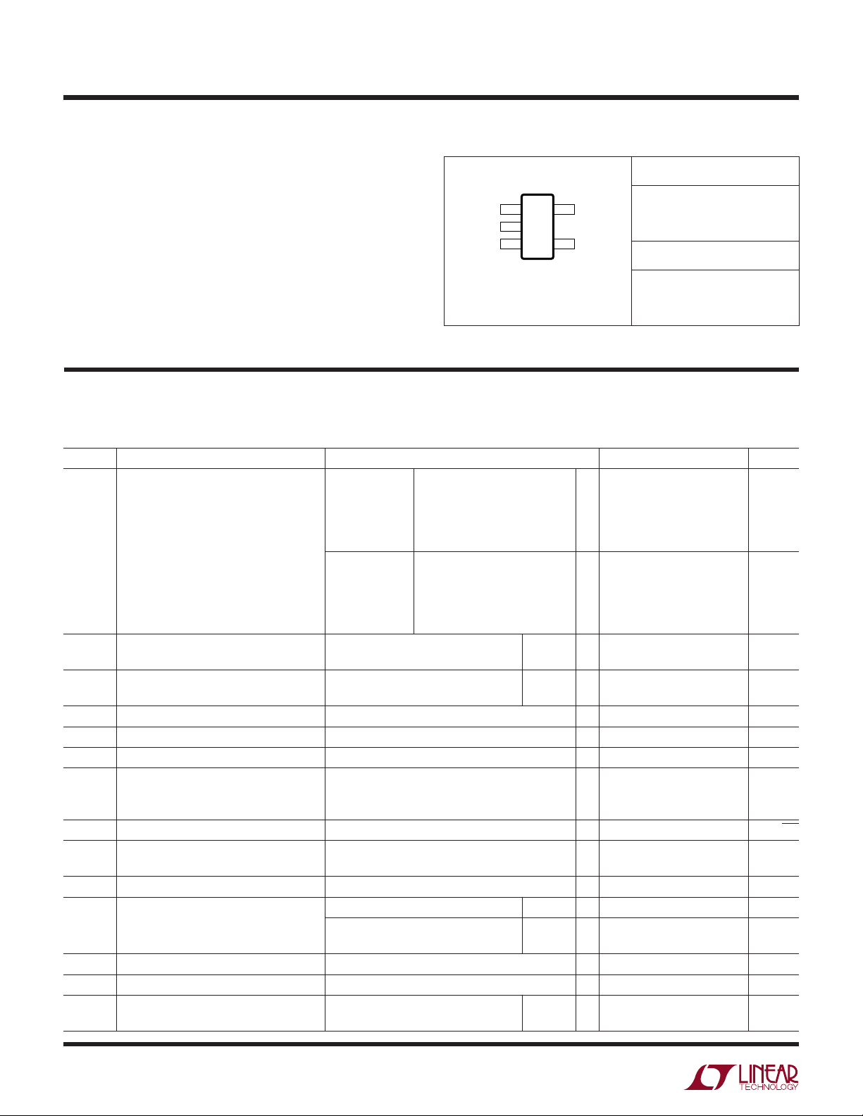
LTC1799
TOP VIEW
S5 PACKAGE
5-LEAD PLASTIC SOT-23
1
2
3
V
+
GND
SET
54OUT
DIV
PACKAGE/ORDER I FOR ATIO
UU
W
WWWU
ABSOLUTE AXI U RATI GS
(Note 1)
Supply Voltage (V+) to GND ........................–0.3V to 6V
DIV to GND ....................................–0.3V to (V+ + 0.3V)
SET to GND ...................................–0.3V to (V+ + 0.3V)
Operating Temperature Range
LTC1799C ............................................... 0°C to 70°C
LTC1799I............................................ – 40°C to 85°C
Storage Temperature Range ................. –65°C to 150°C
Lead Temperature (Soldering, 10 sec)..................300°C
ORDER PART NUMBER
LTC1799CS5
LTC1799IS5
S5 PART MARKING
T
= 125°C, θJA = 256°C/W
JMAX
Consult LTC Marketing for parts specified with wider operating temperature
ranges.
LTND
LTNE
ELECTRICAL CHARACTERISTICS
temperature range, otherwise specifications are at TA = 25°C. V+ = 2.7V to 5.5V, RL=5k, CL = 5pF, unless otherwise noted.
All voltages are with respect to GND.
SYMBOL PARAMETER CONDITIONS MIN TYP MAX UNITS
∆f Frequency Accuracy V+ = 5V 5kHz ≤ f ≤ 20MHz ±0.5 ±1.5 %
(Notes 2, 3) 1kHz ≤ f ≤ 5kHz ±2.5 %
R
SET
f
MAX
f
MIN
∆f/∆T Freq Drift Over Temp (Note 3) R
∆f/∆V Freq Drift Over Supply (Note 3) V+ = 3V to 5V, R
+
V
I
S
V
IH
V
IL
I
DIV
2
Frequency-Setting Resistor Range ∆f < 1.5% V+ = 5V 5 200 kΩ
Maximum Frequency ∆f < 2.5%, Pin 4= 0V V+ = 5V 33 MHz
Minimum Frequency ∆f < 2.5%, Pin 4= V
Timing Jitter Pin 4 = V
(Note 4) Pin 4 = Open 0.13 %
Long-Term Stability of Output Frequency 300 ppm/√kHr
Duty Cycle (Note 7) Pin 4 = V+ or Open (DIV Either by 100 or 10) ● 49 50 51 %
Operating Supply Range ● 2.7 5.5 V
Power Supply Current R
High Level DIV Input Voltage ● V+ – 0.4 V
Low Level DIV Input Voltage ● 0.5 V
DIV Input Current (Note 5) Pin 4 = V
The ● denotes the specifications which apply over the full operating
5kHz ≤ f ≤ 20MHz, LTC1799C
5kHz ≤ f ≤ 20MHz, LTC1799I
20MHz ≤ f ≤ 33MHz ±2.5 %
V+ = 3V 5kHz ≤ f ≤ 10MHz ±0.5 ±1.5 %
5kHz ≤ f ≤ 10MHz, LTC1799C
5kHz ≤ f ≤ 10MHz, LTC1799I
1kHz ≤ f ≤ 5kHz ±2.5 %
10MHz ≤ f ≤ 20MHz ±2.5 %
+
= 3V 10 200 kΩ
V
+
= 3V 20 MHz
V
+
= 31.6k ● ±0.004 %/°C
SET
= 31.6k ● 0.05 0.1 %/V
SET
+
Pin 4 = 0V 0.4 %
Pin 4 = 0V (DIV by 1), R
= 200k, Pin 4 = V+, RL = ∞ V+ = 5V ● 0.7 1.1 mA
SET
R
= 10k, Pin 4 = 0V, RL = ∞ V+ = 5V ● 2.4 mA
SET
+
Pin 4 = 0V V
= 5k to 200k ● 45 50 55 %
SET
+
= 3V ● 2mA
V
V+ = 5V ● 5 8 µA
+
= 5V ● –8 –5 µA
● ±2%
● ±2.5 %
● ±2%
● ±2.5 %
1 kHz
0.06 %
Page 3
LTC1799
ELECTRICAL CHARACTERISTICS
The ● denotes the specifications which apply over the full operating
temperature range, otherwise specifications are at TA = 25°C. V+ = 2.7V to 5.5V, RL=5k, CL = 5pF, Pin 4 = V+ unless otherwise noted.
All voltages are with respect to GND.
SYMBOL PARAMETER CONDITIONS MIN TYP MAX UNITS
V
OH
V
OL
t
r
t
f
Note 1: Absolute Maximum Ratings are those values beyond which the life
of the device may be impaired.
Note 2: Frequencies near 100kHz and 1MHz may be generated using two
different values of R
section). For these frequencies, the error is specified under the following
assumption: 10k < R
is guaranteed by design and test correlation.
Note 3: Frequency accuracy is defined as the deviation from the
f
OSC
High Level Output Voltage (Note 5) V+ = 5V IOH = –1mA ● 4.8 4.95 V
= –4mA ● 4.5 4.8 V
I
OH
V+ = 3V IOH = –1mA ● 2.7 2.9 V
I
= –4mA ● 2.2 2.6 V
OH
Low Level Output Voltage (Note 5) V+ = 5V IOL = 1mA ● 0.05 0.15 V
= 4mA ● 0.2 0.4 V
I
OL
V+ = 3V IOL = 1mA ● 0.1 0.3 V
= 4mA ● 0.4 0.7 V
I
OL
OUT Rise Time V+ = 5V Pin 4 = V+ or Floating, RL = ∞ 14 ns
(Note 6) Pin 4 = 0V, R
V+ = 3V Pin 4 = V+ or Floating, RL = ∞ 19 ns
Pin 4 = 0V, R
OUT Fall Time V+ = 5V Pin 4 = V+ or Floating, RL = ∞ 13 ns
(Note 6) Pin 4 = 0V, R
V+ = 3V Pin 4 = V+ or Floating, RL = ∞ 19 ns
Pin 4 = 0V, R
(see the Table 1 in the Applications Information
SET
equation.
≤ 100k. The frequency accuracy for f
SET
= 20MHz
OSC
= ∞ 7ns
L
= ∞ 11 ns
L
= ∞ 6ns
L
= ∞ 10 ns
L
Note 4: Jitter is the ratio of the peak-to-peak distribution of the period to
the mean of the period. This specification is based on characterization and
is not 100% tested.
Note 5: To conform with the Logic IC Standard convention, current out of
a pin is arbitrarily given as a negative value.
Note 6: Output rise and fall times are measured between the 10% and
90% power supply levels. These specifications are based on
characterization.
Note 7: Guaranteed by 5V test.
3
Page 4
LTC1799
UW
TYPICAL PERFOR A CE CHARACTERISTICS
Frequency Variation
vs R
SET
4
TA = 25°C
GUARANTEED LIMITS APPLY
3
OVER 5k TO 200k RANGE
2
1
0
–1
VARIATION (%)
–2
–3
–4
1 10 100 1000
TYPICAL
HIGH
TYPICAL
LOW
R
(kΩ)
SET
Peak-to-Peak Jitter vs Frequency
0.7
0.6
0.5
0.4
0.3
JITTER (%)
0.2
0.1
0
1k 100k 1M 10M
÷10
÷100
10k
OUTPUT FREQUENCY, f
÷1
OUT
(Hz)
1799 G01
100M
1799 G03
Frequency Variation
Over Temperature
1.00
R
= 31.6k
SET
÷1 OR ÷10 OR ÷100
0.75
0.50
0.25
0
–0.25
VARIATION (%)
–0.50
–0.75
–1.00
–40
TYPICAL
HIGH
TYPICAL
LOW
–20 0
TEMPERATURE (°C)
40 80
20 60
Supply Current
vs Output Frequency
4.5
TA = 25°C
= 5pF
C
4.0
L
= 1M
R
L
3.5
3.0
2.5
2.0
1.5
SUPPLY CURRENT (mA)
1.0
0.5
0
÷100 (5V)
÷100 (3V)
1k 100k 1M 100M
÷10 (3V)
10k
OUTPUT FREQUENCY, f
÷1 (5V)
÷10 (5V)
÷1 (3V)
OUT
1799 G02
10M
(Hz)
1799 G04
Output Resistance
vs Supply Voltage
140
120
100
80
OUTPUT RESISTANCE (Ω)
60
OUTPUT SINKING CURRENT
40
2.5 3.0
4
= 25°C
T
A
OUTPUT SOURCING CURRENT
4.5
4.0
3.5
SUPPLY VOLTAGE (V)
5.0
5.5
1799 G05
6.0
LTC1799 Output Operating at
20MHz, VS = 5V
V+ = 5V, R
1V/DIV
= 5k, CL = 10pF V+ = 3V, R
SET
12.5ns/DIV
1799 G06
LTC1799 Output Operating at
10MHz, VS = 3V
= 10k, CL = 10pF
SET
1V/DIV
25ns/DIV
1799 G07
Page 5

LTC1799
U
UU
PI FU CTIO S
V+ (Pin 1): Voltage Supply (2.7V ≤ V+ ≤ 5.5V). This supply
must be kept free from noise and ripple. It should be
bypassed directly to a ground plane with a 0.1µF capacitor.
GND (Pin 2): Ground. Should be tied to a ground plane for
best performance.
SET (Pin 3): Frequency-Setting Resistor Input. The value
of the resistor connected between this pin and V+ determines the oscillator frequency. The voltage on this pin is
held by the LTC1799 to approximately 1.13V below the V
voltage. For best performance, use a precision metal film
resistor with a value between 10k and 200k and limit the
capacitance on this pin to less than 10pF.
DIV (Pin 4): Divider-Setting Input. This three-state input
selects among three divider settings, determining the
value of N in the frequency equation. Pin 4 should be tied
to GND for the ÷1 setting, the highest frequency range.
+
Floating Pin 4 divides the master oscillator by 10. Pin 4
should be tied to V+ for the ÷100 setting, the lowest
frequency range. To detect a floating DIV pin, the LTC1799
attempts to pull the pin toward midsupply. This is realized
with two internal current sources, one tied to V+ and Pin
4 and the other one tied to ground and Pin 4. Therefore,
driving the DIV pin high requires sourcing approximately
5µA. Likewise, driving DIV low requires sinking 5µA.
When Pin 4 is floated, preferably it should be bypassed by
a 1nF capacitor to ground or it should be surrounded by a
ground shield to prevent excessive coupling from other
PCB traces.
OUT (Pin 5): Oscillator Output. This pin can drive 5kΩ
and/or 10pF loads. Larger loads may cause inaccuracies
due to supply bounce at high frequencies. Transients will
not cause latchup if the current into/out of the OUT pin is
limited to 50mA.
BLOCK DIAGRA
+
V
1
R
SET
I
RES
SET
3
+
V
BIAS
–
GND
W
I
+
–
RES
GAIN = 1
= 1.13V ±25%
V
RES
+
(V
– V
SET
)
ƒ
MO
MASTER OSCILLATOR
= 100MHz • kΩ •
(V+ – V
PROGRAMMABLE
DIVIDER
(÷1, 10 OR 100)
I
RES
)
SET
DIVIDER
SELECT
THREE-STATE
INPUT DETECT
V
GND
+
OUT
DIV
5
5µA
42
5µA
1799 BD
5
Page 6

LTC1799
THEORY OF OPERATIO
U
As shown in the Block Diagram, the LTC1799’s master
oscillator is controlled by the ratio of the voltage between
the V+ and SET pins and the current entering the SET pin
(I
). The voltage on the SET pin is forced to approxi-
RES
mately 1.13V below V+ by the PMOS transistor and its gate
bias voltage. This voltage is accurate to ±7% at a particular
input current and supply voltage (see Figure 1). The
effective input resistance is approximately 2k.
A resistor R
“locks together” the voltage (V+ – V
, connected between the V+ and SET pins,
SET
) and current, I
SET
RES
,
variation. This provides the LTC1799’s high precision. The
master oscillation frequency reduces to:
ƒ=
MO
10
MHz
•
10
R
k
SET
Ω
The LTC1799 is optimized for use with resistors between
10k and 200k, corresponding to master oscillator frequencies between 0.5MHz and 10MHz. Accurate frequencies up to 20MHz (R
= 5k) are attainable if the supply
SET
voltage is greater than 4V.
To extend the output frequency range, the master oscilla-
tor signal may be divided by 1, 10 or 100 before driving
OUT (Pin 5). The divide-by value is determined by the state
of the DIV input (Pin 4). Tie DIV to GND or drive it below
0.5V to select ÷1. This is the highest frequency range, with
the master output frequency passed directly to OUT. The
DIV pin may be floated or driven to midsupply to select
÷10, the intermediate frequency range. The lowest frequency range, ÷100, is selected by tying DIV to V+ or
driving it to within 0.4V of V+. Figure 2 shows the relationship between R
, divider setting and output frequency,
SET
including the overlapping frequency ranges near 100kHz
and 1MHz.
The CMOS output driver has an on resistance that is
typically less than 100Ω. In the ÷1 (high frequency) mode,
the rise and fall times are typically 7ns with a 5V supply and
11ns with a 3V supply. These times maintain a clean
square wave at 10MHz (20MHz at 5V supply). In the ÷10
and ÷100 modes, where the output frequency is much
lower, slew rate control circuitry in the output driver
increases the rise/fall times to typically 14ns for a 5V
supply and 19ns for a 3V supply. The reduced slew rate
lowers EMI (electromagnetic interference) and supply
bounce.
1.4
1.3
1.2
SET
– V
+
1.1
= V
RES
V
1.0
0.9
0.8
1
Figure 1. V+ – V
TA = 25°C
V+ = 5V
V+ = 3V
10 100 1000
I
(µA)
RES
Variation with I
SET
1799 F01
RES
1000
100
(kΩ)
SET
R
10
1
1k 100k 1M 10M
Figure 2. R
÷100 ÷10 ÷1
10k
DESIRED OUTPUT FREQUENCY (Hz)
vs Desired Output Frequency
SET
MOST
ACCURATE
OPERATION
100M
1799 F02
6
Page 7

WUUU
APPLICATIO S I FOR ATIO
LTC1799
SELECTING THE DIVIDER SETTING AND RESISTOR
The LTC1799’s master oscillator has a frequency range
spanning 0.1MHz to 33MHz. However, accuracy may
suffer if the master oscillator is operated at greater than
10MHz with a supply voltage lower than 4V. A programmable divider extends the frequency range to greater than
three decades. Table 1 describes the recommended frequencies for each divider setting. Note that the ranges
overlap; at some frequencies there are two divider/resistor
combinations that result in the desired frequency.
In general, any given oscillator frequency (f
) should be
OSC
obtained using the lowest master oscillator frequency.
Lower master oscillator frequencies use less power and
are more accurate. For instance, f
obtained by either R
= 10MHz or R
The R
= 100k is preferred for lower power and better
SET
= 100k, N = 10, master oscillator = 1MHz.
SET
= 10k, N = 100, master oscillator
SET
= 100kHz can be
OSC
accuracy.
Table 1. Frequency Range vs Divider Setting
DIVIDER SETTING FREQUENCY RANGE
< 100kHz
< 10kΩ), the
SET
*
÷1 ⇒ DIV (Pin 4) = GND >500kHz
÷10 ⇒ DIV (Pin 4) = Floating 50kHz to 1MHz
÷100 ⇒ DIV (Pin 4) = V
*
At master oscillator frequencies greater than 10MHz (R
LTC1799 may suffer reduced accuracy with a supply voltage less than 4V.
+
After choosing the proper divider setting, determine the
correct frequency-setting resistor. Because of the linear
correspondence between oscillation period and resistance, a simple equation relates resistance with frequency.
ALTERNATIVE METHODS OF SETTING THE OUTPUT
FREQUENCY OF THE LTC1799
The oscillator may be programmed by any method that
sources a current into the SET pin (Pin 3). The circuit in
Figure 3 sets the oscillator frequency using a programmable current source and in the expression for f
resistor R
is replaced by the ratio of 1.13V/I
SET
CONTROL
OSC
, the
. As
already explained in the “Theory of Operation,” the voltage
difference between V+ and SET is approximately 1.13V,
therefore, the Figure 3 circuit is less accurate than if a
resistor controls the oscillator frequency.
Figure 4 shows the LTC1799 configured as a VCO. A
voltage source is connected in series with an external 10k
resistor. The output frequency, f
V
CONTROL
, that is the voltage source connected between
, will vary with
OSC
V+ and the SET pin. Again, this circuit decouples the
relationship between the input current and the voltage
between V+ and SET; the frequency accuracy will be
degraded. The oscillator frequency, however, will monotonically increase with decreasing V
+
I
CONTROL
5µA TO 200µA
V
0.1µF
ƒ
≅
OSC
I
CONTROL
1
+
OUT
V
LTC1799
2
GND
3
SET
1799 F03
10MHz
10kΩ
••I
N
1.13V
EXPRESSED IN (A)
CONTROL
400kHz TO 21MHz
(APPROXIMATE, SEE TEXT)
5
4
N = 1
DIV
CONTROL
.
Rk
=
10
SET
(R
SETMIN
R
SETMAX
Any resistor, R
oscillator, f
•
= 3k (5V Supply), 5k (3V Supply),
= 1M)
SET
.
OSC
100
10
Nf
MHz
•
OSC
, N =
10
1
, tolerance adds to the inaccuracy of the
V
CONTROL
0V TO 1.13V
Figure 3. Current Controlled Oscillator
+
V
0.1µF
+
–
R
SET
10k
1
+
V
LTC1799
2
GND
3
SET
10MHz
≅
ƒ
OSC
• • 1 –
N
5
OUT
4
N = 1
DIV
1799 F04
10k
R
V
CONTROL
()
SET
1.13V
Figure 4. Voltage Controlled Oscillator
7
Page 8

LTC1799
WUUU
APPLICATIO S I FOR ATIO
POWER SUPPLY REJECTION
Low Frequency Supply Rejection (Voltage Coefficient)
Figure 5 shows the output frequency sensitivity to power
supply voltage at several different temperatures. The
LTC1799 has a conservative guaranteed voltage coefficient of 0.1%/V but, as Figure 5 shows, the typical supply
sensitivity is lower.
0.15
R
= 31.6k
SET
PIN 4 = FLOATING (÷10)
0.10
25°C
0.05
0
FREQUENCY DEVIATION (%)
–0.05
2.5
3.0 3.5 4.0 4.5
SUPPLY VOLTAGE (V)
–40°C
85°C
5.0 5.5
1799 F05
START-UP TIME
The start-up time and settling time to within 1% of the final
value can be estimated by t
20µs. Note the start-up time depends on R
START
≅ R
(2.8µs/kΩ) +
SET
and it is
SET
independent from the setting of the divider pin. For instance with R
= 50k, the LTC1799 will settle with 1% of
SET
its 200kHz final value (N = 10) in approximately 160µs.
Figure 6 shows start-up times for various R
resistors.
SET
Figure 7 shows an application where a second set resistor
R
is connected in parallel with set resistor R
SET2
SET1
via
switch S1. When switch S1 is open, the output frequency
of the LTC1799 depends on the value of the resistor R
SET1
.
When switch S1 is closed, the output frequency of the
LTC1799 depends on the value of the parallel combination
of R
SET1
and R
SET2
.
The start-up time and settling time of the LTC1799 with
switch S1 open (or closed) is described by t
START
shown
above. Once the LTC1799 starts and settles, and switch S1
closes (or opens), the LTC1799 will settle to its new output
frequency within approximately 25µs.
Figure 5. Supply Sensitivity
High Frequency Power Supply Rejection
The accuracy of the LTC1799 may be affected when its
power supply generates significant noise with frequency
contents in the vicinity of the programmed value of f
OSC
.
If a switching power supply is used to power up the
LTC1799, and if the ripple of the power supply is more than
a few tens of millivolts, make sure the switching frequency
and its harmonics are not related to the output frequency
of the LTC1799. Otherwise, the oscillator may show an
additional 0.1% to 0.2% of frequency error.
If the LTC1799 is powered by a switching regulator and the
switching frequency or its harmonics coincide with the
output frequency of the LTC1799, the jitter of the oscillator
output may be affected. This phenomenon will become
noticeable if the switching regulator exhibits ripples beyond 30mV.
FREQUENCY ERROR (%)
3V OR 5V
S1
R
SET1
R
SET2
–10
60
50
40
30
20
10
0
0
200k
10k
31.6k
100 200
TIME AFTER POWER APPLIED (µs)
Figure 6. Start-Up Time
1
+
V
OUT
LTC1799
2
GND
3
SET
DIV
400 600
300 500
5
+
V
÷100
4
÷10
÷1
1799 F07
TA = 25°C
V
f
OSC
OR
f
OSC
+
= 5V
1799 F06
= 10MHz •
= 10MHz •
10k
()
N • R
SET1
10k
()
N • R
//R
SET1
SET2
8
Figure 7
Page 9

WUUU
APPLICATIO S I FOR ATIO
LTC1799
Jitter
The typical jitter is listed in the Electrical Characteristics
and shown in the Typical Performance Characteristics.
These specifications assume that the capacitance on SET
U
TYPICAL APPLICATIO S
Low Power 80Hz to 8kHz Sine Wave Generator (IQ < 4mA)
0.1µF
3V
C1
R
SET
1
+
V
LTC1799
2
GND
3
SET
800Hz ≤ f
80Hz ≤ f
5
OUT
SW1
4
DIV
0.1µF
≤ 8kHz, N = 10
SINE
≤ 800Hz, N = 100
SINE
3V
OPEN, N = 10
C2
3V, N = 100
3V
f
OSC
C4
1µF
÷2
÷4
÷8
÷16
÷32
÷64
÷128
÷256
1
2
16
10
7
8
9
15
74HC4520
CLOCK A
ENABLE A
V
DD
ENABLE B
RESET A
V
SS
CLOCK B
RESET B
Q1A
Q2A
Q3A
Q4A
Q1B
Q2B
Q3B
Q4B
3
4
5
6
11
12
13
14
(Pin 3) is limited to less than 10pF, as suggested in the Pin
Functions description. If this requirement is not met, the
jitter will increase. For more information, contact Linear
Technology Applications group.
1
2
3
4
5
6
7
8
V
NC
V
SA
LPA
BPA
HPA/NA
INV A
LTC1067-50
+
+
R
249k
H1
51.1k
R
L1
CLK
AGND
LPB
BPB
HPB/NB
INV B
16
15
R62 14k
14
–
V
13
SB
12
11
10
9
R32 51.1k
R22 20k
R52
5.11k
SINEWAVE
OUT
f
SINE
1799 TA05
10MHz
= •
N
64R
100k
f
OSC
R11
64
R61
10k
3V
0.1µF
C3
R51 5.11k
R31 51.1k
R21 20k
10k
SET
CLOCK-TUNABLE LOWPASS FILTER WITH
A STOPBAND NOTCH AT THE 3rd HARMONIC
f
OSC
• 3
()
64
9
Page 10

LTC1799
TYPICAL APPLICATIO S
3V Digitally Controlled Oscillator with 5kHz to 85kHz Range (N = 100, Pin 4 = V+)
3V
U
CLK
D
CS/LD
LTC1659
1
CLK
2
D
10k
10k
IN
3
CS/LD
4
D
OUT
3V
R1
10
R2
9
R3
10k
NOTES:
1. FOR N = 10 (PIN 4 OPEN) THE RANGE IS 50kHz TO 850kHz
2. FOR N = 1 (PIN 4 = GND) THE RANGE IS 500kHz TO 8.5MHz
3. DRIVING PIN 4 OF THE LTC1799 WITH A 3-STATE LOGIC DEVICE
GIVES A RANGE OF 5kHz TO 8.5MHz
IN
V
CC
V
OUT
REF
GND
+
1/4 LT1491
–
R4
10k
8
7
6
5
C3
0.1µF
3V
R5
10k
R6
10k
8
R7
10k
R8
10k
3
2
7
+
1/4 LT1491
–
1/4 LT1491
C2
0.1µF
4
1
11
5kHz TO 85kHz
1
3V
R
S
10k
5
+
6
–
I =
(V+ – V
10k
SET
C1
0.1µF
)
•
4096
+
V
LTC1799
2
GND
3
SET
C
C: DAC CODE 200 ≤ C ≤ 3480
OUT
DIV
5
f
OSC
4
1799 TA06
OUT
= 100kHz •
3V
C
4096
10
Input Code vs Output Frequency
(N = 100, Pin 4 = V+)
100
75
(kHz)
50
OUT
f
25
0
0 1024 2048 3072 4096
DAC CODE
1799 TA07
Page 11

PACKAGE DESCRIPTIO
LTC1799
U
S5 Package
5-Lead Plastic SOT-23
(Reference LTC DWG # 05-08-1633)
(Reference LTC DWG # 05-08-1635)
2.80 – 3.10
(.110 – .118)
(NOTE 3)
SOT-23
(Original)
.90 – 1.45
A
(.035 – .057)
.00 – .15
A1
(.00 – .006)
.90 – 1.30
A2
(.035 – .051)
.35 – .55
L
(.014 – .021)
.20
(.008)
DATUM ‘A’
L
NOTE:
1. CONTROLLING DIMENSION: MILLIMETERS
2. DIMENSIONS ARE IN
3. DRAWING NOT TO SCALE
4. DIMENSIONS ARE INCLUSIVE OF PLATING
5. DIMENSIONS ARE EXCLUSIVE OF MOLD FLASH AND METAL BURR
6. MOLD FLASH SHALL NOT EXCEED .254mm
7. PACKAGE EIAJ REFERENCE IS:
SC-74A (EIAJ) FOR ORIGINAL
JEDEL MO-193 FOR THIN
SOT-23
(ThinSOT)
1.00 MAX
(.039 MAX)
.01 – .10
(.0004 – .004)
.80 – .90
(.031 – .035)
.30 – .50 REF
(.012 – .019 REF)
MILLIMETERS
(INCHES)
2.60 – 3.00
(.102 – .118)
.09 – .20
(.004 – .008)
(NOTE 2)
1.50 – 1.75
(.059 – .069)
(NOTE 3)
PIN ONE
A
.95
(.037)
REF
A2
1.90
(.074)
REF
.25 – .50
(.010 – .020)
(5PLCS, NOTE 2)
A1
S5 SOT-23 0401
Information furnished by Linear Technology Corporation is believed to be accurate and reliable.
However, no responsibility is assumed for its use. Linear Technology Corporation makes no representation that the interconnection of its circuits as described herein will not infringe on existing patent rights.
11
Page 12

LTC1799
1799 TA04
1400
1200
1000
800
600
400
200
0
–20–100 102030405060708090
TEMPERATURE (°C)
FREQUENCY (kHz)
MAX
TYP
MIN
TYPICAL APPLICATIO S
U
ON/SHDN
Shutting Down the LTC1799
5V
74AC04
R1
10k
C1
0.1µF
1
2
3
+
V
LTC1799
GND
SET
OUT
DIV
1799 TA08
5
OUT
4
100k
THERMISTOR
Temperature-to-Frequency Converter
5V
R
C1
T
0.1µF
: YSI 44011 800 765-4974
R
T
1
2
3
+
V
LTC1799
GND
SET
OUT
DIV
5
4
1799 TA03
f
OSC
=
10MHz
10
Output Frequency vs Temperature
10k
•
R
T
12
Linear Technology Corporation
1630 McCarthy Blvd., Milpitas, CA 95035-7417
(408) 432-1900 ● FAX: (408) 434-0507
●
www.linear.com
1799f LT/TP 0801 2K • PRINTED IN USA
LINEAR TECHNOLOGY CORPORATION 2001
 Loading...