

Page 1
LTC1771
Final Electrical Specifications
Low Quiescent Current
High Efficiency Step-Down
DC/DC Controller
FEATURES
■
Very Low Standby Current: 10µA
■
Available in Space-Saving 8-Lead MSOP Package
■
High Output Currents
■
Wide VIN Range: 2.8V to 20V Operation
■
V
Range: 1.23V to 18V
OUT
■
High Efficiency: Over 93% Possible
■
±2% Output Accuracy
■
Very Low Dropout Operation: 100% Duty Cycle
■
Current Mode Operation for Excellent Line and
Load Transient Response
■
Defeatable Burst ModeTM Operation
■
Short-Circuit Protected
■
Optional Programmable Soft-Start
■
Micropower Shutdown: IQ = 2µA
U
APPLICATIO S
■
Cellular Telephones and Wireless Modems
■
1- to 4-Cell Lithium-Ion-Powered Applications
■
Portable Instruments
■
Battery-Powered Equipment
■
Battery Chargers
■
Scanners
U
February 2000
DESCRIPTIO
The LTC®1771 is a high efficiency current mode stepdown DC/DC controller that draws as little as 10µA DC
supply current to regulate the output at no load while
maintaining high efficiency for loads up to several amps.
The LTC1771 drives an external P-channel power MOSFET
using a current mode, constant off-time architecture. An
external sense resistor is used to program the operating
current level. Current mode control provides short-circuit
protection, excellent transient response and controlled
start-up behavior. Burst Mode operation enables the
LTC1771 to maintain high efficiency down to extremely
low currents. Shutdown mode further reduces the supply
current to a mere 2µA. For low noise applications, Burst
Mode operation can be easily disabled with the MODE pin.
Wide input supply range of 2.8V to 18V (20V maximum)
and 100% duty cycle operation for low dropout make the
LTC1771 ideal for a wide variety of battery-powered applications where maximizing battery life is important.
The LTC1771’s availability in both 8-lead MSOP and SO
packages provides for a minimum area solution.
, LTC and LT are registered trademarks of Linear Technology Corporation.
Burst Mode is a trademark of Linear Technology Corporation.
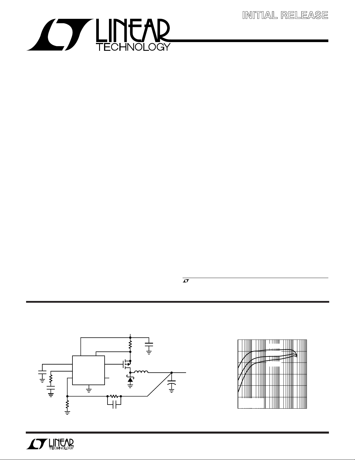
TYPICAL APPLICATIO
V
IN
C
SS
0.01µF
R
C
10k
C
22OpF
RUN/SS
I
TH
V
FB
C
R1
1M
1%
Figure 1. High Efficiency Step-Down Converter
LTC1771
GND
U
V
IN
4.5V TO 18V
100
90
80
70
EFFICIENCY (%)
60
50
40
L1
15µH
10µF
25V
CER
V
OUT
3.3V
C
OUT
150µF
6.3V
2A
1771 F01
+
R
SENSE
0.05Ω
SENSE
PGATE
MODE
M1
Si6447DQ
V
IN
R2
1.64M
1%
5pF
Information furnished by Linear Technology Corporation is believed to be accurate and reliable.
However, no responsibility is assumed for its use. Linear Technology Corporation makes no representation that the interconnection of its circuits as described herein will not infringe on existing patent rights.
UPS5817
LTC1771 Efficiency
VIN = 5V
VIN = 10V
VIN = 15V
V
= 3.3V
OUT
= 0.05Ω
R
SENSE
0.1 1 100 1000 10000
10
LOAD CURRENT (mA)
1771 F01b
1
Page 2
LTC1771
RUN/SS
I
TH
V
FB
GND
1
2
3
4
8
7
6
5
MODE
SENSE
V
IN
PGATE
TOP VIEW
MS8 PACKAGE
8-LEAD PLASTIC MSOP
TOP VIEW
MODE
SENSE
V
IN
PGATE
RUN/SS
I
TH
V
FB
GND
S8 PACKAGE
8-LEAD PLASTIC SO
1
2
3
4
8
7
6
5
WWWU
ABSOLUTE AXI U RATI GS
(Note 1)
Input Supply Voltage (VIN)........................ –0.3V to 20V
Peak Driver Output Current < 10µs (PGATE) ............. 1A
RUN/SS Voltage ........................... – 0.3V to (VIN + 0.3V)
MODE Voltage .......................................... –0.3V to 20V
ITH, VFB Voltage .......................................... –0.3V to 5V
SENSE Voltage (VIN > 12V)...(VIN – 12V) to (VIN + 0.3V)
SENSE Voltage (VIN ≤ 12V) .......... –0.3V to (VIN + 0.3V)
UU
W
PACKAGE/ORDER I FOR ATIO
ORDER PART
NUMBER
LTC1771EMS8
MS8 PART MARKING
T
= 125°C, θJA = 150°C/W
JMAX
LTKD
Junction Temperature (Note 2)............................ 125°C
Operating Temperature Range (Note 3)
LTC1771E......................................... –40°C to 85°C
LTC1771I ......................................... – 40°C to 85°C
Storage Temperature Range ................. –65°C to 150°C
Lead Temperature (Soldering, 10 sec).................. 300°C
ORDER PART
NUMBER
LTC1771ES8
LTC1771IS8
S8 PART MARKING
T
= 125°C, θJA = 110°C/W
JMAX
1771
1771I
Consult factory for Military grade parts.
ELECTRICAL CHARACTERISTICS
The ● denotes specifications which apply over the full operating temperature range, otherwise specifications are TA = 25°C.
VIN = 10V, V
SYMBOL PARAMETER CONDITIONS MIN TYP MAX UNITS
V
FB
I
FB
I
SUPPLY
∆V
LINEREG
∆V
LOADREG
I
Q
∆V
SENSE(MAX)
∆V
SENSE(MIN)
∆V
SENSE(SLEEP)
t
OFF
V
MODE
2
= open unless otherwise specified.
RUN
Feedback Voltage (Note 5) ● 1.205 1.230 1.255 V
Feedback Current (Note 5) ● 110 nA
No-Load Supply Current VIN = 10V, I
Reference Voltage Line Regulation VIN = 5V to 15V (Note 5) ● 0.003 0.03 %/V
Output Voltage Load Regulation ITH = 0.5V to 2V, Burst Disabled (Note 5) ● 0.25 1 %
Input DC Supply Current (Note 4)
Active Mode (PGATE = 0V) V
Sleep Mode (Note 6) V
Shutdown V
Short Circuit V
Maximum Current Sense Threshold VFB = V
Minimum Current Sense Threshold VFB = V
Sleep Current Sense Threshold ITH = 1V 50 mV
Switch Off Time VFB at Regulated Value 3.5 µs
Mode Pin Threshold V
= 2.8V to 18V 150 235 µA
IN
= 2.8V to 18V, VFB = 1.5V 9 15 µA
IN
= 2.8V to 18V, V
IN
= 2.8V to 18V, VFB = 0V 175 275 µA
IN
REF
REF
= 0V 70 µs
V
FB
Rising ● 0.5 1.3 2 V
MODE
= 0 (Note 6) 10 µA
LOAD
= 0V 2 6 µA
RUN
– 20mV ● 110 140 180 mV
+ 10mV, Burst Disabled –25 mV
Page 3
LTC1771
ELECTRICAL CHARACTERISTICS
The ● denotes specifications which apply over the full operating temperature range, otherwise specifications are TA = 25°C.
VIN = 10V, V
SYMBOL PARAMETER CONDITIONS MIN TYP MAX UNITS
V
RUN/SS
I
RUN
PGATE tr, t
= open unless otherwise specified.
RUN
RUN/SS Pin Threshold V
Source Current V
PGATE Transition Time (Note 7)
f
Rise Time C
Fall Time C
Rising ● 0.5 1.0 2 V
RUN/SS
= 0V, VIN = 2.8V to 18V 0.3 1 3 µA
RUN
= 2000pF 80 ns
LOAD
= 2000pF 90 ns
LOAD
Note 1: Absolute Maximum Ratings are those values beyond which the life
of a device may be impaired.
Note 2: T
dissipation P
Note 3: The LTC1771E is guaranteed to meet performance specifications
from 0°C to 70°C. Specifications over the –40°C to 85°C operating
temperature range are assured by design, characterization and correlation
with statistical process controls. The LTC1771I is guaranteed and tested
over the –40°C to 85°C operating temperature range.
is calculated from the ambient temperature TA and power
J
according to the following formulas:
D
LTC1771S8: TJ = TA + (PD)(110°C/W)
LTC1771MS8: T
U
= TA + (PD)(150°C/W)
J
UU
PI FU CTIO S
RUN/SS (Pin 1): The voltage level on this pin controls
shutdown/run mode (ground = shutdown, open/high =
run). Connecting an external capacitor to this pin provides
soft-start.
ITH (Pin 2): Error Amplifier Compensation Point. The
current comparator threshold increases with this control
voltage. Nominal voltage range for this pin is 0V to 3V.
VFB (Pin 3): Feedback of Output Voltage for Comparison
to Internal 1.23V Reference. An external resistive divider
across the output is returned to this pin.
GND (Pin 4): Ground Pin.
Note 4: Dynamic supply current is higher due to the gate charge being
delivered at the switching frequency. See Applications Information.
Note 5: The LTC1771 is tested in a feedback loop that servos V
balance point for the error amplifier (V
Note 6: No-load supply current consists of sleep mode current (9µA
typical) plus a small switching component necessary to overcome
Schottky diode leakage and feedback resistor current.
Note 7: t
and tf measured at 10% to 90% levels.
r
= 1.23V).
ITH
to the
FB
PGATE (Pin 5): High Current Gate Driver for External
P-Channel MOSFET Switch. Voltage swing is from ground
to VIN.
VIN (Pin 6): Main Input Voltage Supply Pin.
SENSE (Pin 7): Current Sense Input for Monitoring Switch
Current. Maximum switch current and Burst Mode
threshold is programmed with an external resistor between SENSE and VIN.
MODE (Pin 8): Burst Mode Enable/Disable Pin. Connecting this pin to VIN (or above 2V) enables Burst Mode
operation, while connecting this pin to ground disables
Burst Mode operation. Do not leave floating.
3
Page 4
LTC1771
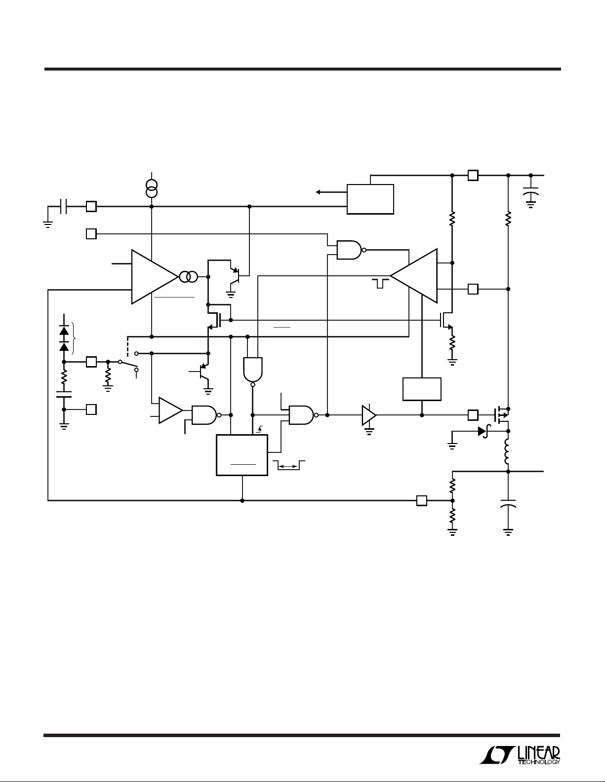
UU
W
FUNCTIONAL BLOCK DIAGRA
V
IN
+
EA
–
1V
1V
1µA
ON
10% CURRENT
–
B
+
SOFT-START
2V
C
SS
RUN/SS
1
MODE
(BURST ENABLE)
8
1.23V
V
OUT
*
I
TH
2
R
C
C
C
GND
4
SLEEP
READY
READY
1.23V
REFERENCE
10% CURRENT
V
IN
C
ON
BLANKING
22k R
–
+
250k
V
IN
6
SENSE
7
SW
5
+
SENSE
V
IN
C
IN
*
OPTIONAL FOR FOLDBACK
CURRENT LIMITING
MODE
ON TRIGGER
1-SHOT
STRETCH
3.5µs
L
V
OUT
V
FB
3
+
C
OUT
1771 BD
4
Page 5

OPERATIO
LTC1771
U
(Refer to Functional Block Diagram)
Main Control Loop
The LTC1771 uses a constant off-time, current mode
step-down architecture. During normal operation, the
P-channel MOSFET is turned on at the beginning of each
cycle and turned off when the current comparator C
triggers the 1-shot timer. The external MOSFET switch
stays off for the 3.5µs 1-shot duration and then turns back
on again to begin a new cycle. The peak inductor current
at which C triggers the 1-shot is controlled by the voltage
on Pin 3 (ITH), the output of the error amplifier EA. An
external resistive divider connected between V
ground allows EA to receive an output feedback voltage
VFB. When the load current increases, it causes a slight
decrease in VFB relative to the 1.23V reference, which in
turn causes the ITH voltage to increase until the average
inductor current matches the new load current.
The main control loop is shut down by pulling Pin 1
(RUN/SS) low. Releasing RUN/SS allows an internal 1µA
current source to charge soft-start capacitor CSS. When
CSS reaches 1V, the main control loop is enabled with the
ITH voltage clamped at approximately 40% of its maximum value. As CSS continues to charge, ITH is gradually
released allowing normal operation to resume.
Burst Mode Operation
The LTC1771 provides outstanding low current efficiency
and ultralow no-load supply current by using Burst Mode
operation when the MODE pin is pulled above 2V. During
Burst Mode operation, short burst cycles of normal switching are followed by a longer idle period with the switch off
and the load current is supplied by the output capacitor.
During this idle period, only the minimum required circuitry—1.23V reference and error amp—are left on, and
the supply current is reduced to 9µA. At no load, the output
capacitor is still discharged very slowly by leakage current
in the Schottky diode and feedback resistor current resulting in very low frequency burst cycles that add a few more
microamps to the supply current.
OUT
and
Burst Mode operation is provided by clamping the minimum ITH voltage at 1V which represents about 25% of
maximum load current. If the load falls below this level, i.e.
the ITH voltage tries to fall below 1V, the burst comparator
B switches state signaling the LTC1771 to enter sleep
mode. During this time, EA is reduced to 10% of its normal
operating current and the external compensation capacitor is disconnected and clamped to 1V so that the EA can
drive its output with the lower available current. As the load
discharges the output capacitor, the internal ITH voltage
increases. When it exceeds 1V the burst comparator exits
sleep mode, reconnects the external compensation components to the error amplifier output, and returns EA to full
power along with the other necessary circuitry. This
scheme (patent pending) allows the EA to be reduced to
such a low operating current during sleep mode without
adding unacceptable delay to wake up the LTC1771 due to
the compensation capacitor on ITH required for stability in
normal operation.
Burst Mode operation can be disabled by pulling the
MODE pin to ground. In this mode of operation, the burst
comparator B is disabled and the ITH voltage allowed to go
all the way to 0V. The load can now be reduced to about 1%
of maximum load before the loop skips cycles to maintain
regulation. This mode provides a low noise output spectrum, useful for reducing both audio and RF interference,
at the expense of reduced efficiency at light loads.
Off-Time
The off-time duration is 3.5µs when the feedback voltage
is close to the reference voltage; however, as the feedback
voltage drops, the off-time lengthens and reaches a maximum value of about 70µs when VFB is zero. This ensures
that the inductor current has enough time to decay when
the reverse voltage across the inductor is low such as
during short circuit, thus protecting the MOSFET and
inductor.
5
Page 6

LTC1771
WUUU
APPLICATIO S I FOR ATIO
The basic LTC1771 application circuit is shown in Figure
1 on the first page. External component selection is driven
by the load requirement and begins with the selection of
R
SENSE
. Once R
is known, L can be chosen. Next, the
SENSE
MOSFET and D1 are selected. The inductor is chosen
based largely on the desired amount of ripple current and
for Burst Mode operation. Finally CIN is selected for its
ability to handle the required RMS input current and C
OUT
is chosen with low enough ESR to meet the output voltage
ripple and transient specifications.
R
R
Selection
SENSE
is chosen based on the required output current.
SENSE
The LTC1771 current comparator has a maximum threshold of 140mV/R
. The current comparator threshold
SENSE
sets the peak inductor current, yielding a maximum average output current I
equal to the peak less half the
MAX
peak-to-peak ripple current ∆IL. For best performance
when Burst Mode operation is enabled, choose ∆IL equal
to 35% of peak current. Allowing a margin for variations in
the LTC1771 and external components gives the following
equation for choosing R
R
SENSE
= 100mV/I
MAX
SENSE
:
At higher supply voltages, the peak currents may be
slightly higher due to overshoot from current comparator
delay and can be predicted from the second term in the
following equation:
12
.
I
PEAK
014
≅+
R
SENSE
.
05
VV
–
IN OUT
LH
µ
()
/
Inductor Value Selection
Once R
is known, the inductor value can be deter-
SENSE
mined. The inductance value has a direct effect on ripple
current. The ripple current decreases with higher inductance and increases with higher V
. The ripple current
OUT
during continuous mode operation is set by the off-time
and inductance to be:
VV
∆=
It
L CONT OFF
()
Kool Mµ is a registered trademark of Magnetics, Inc.
OUT D
+
L
where t
= 3.5µs. However, the ripple current at low
OFF
loads during Burst Mode operation is:
∆I
L(BURST)
≈ 35% of I
PEAK
≈ 0.05/R
SENSE
For best efficiency when Burst Mode operation is enabled,
choose:
∆I
L(CONT)
≤ ∆I
L(BURST)
so that the inductor current is continuous during the burst
periods. This sets a minimum inductor value of:
L
= (70µH)(V
MIN
When burst is disabled, ripple currents less than ∆I
can be achieved by choosing L > L
OUT
+ VD)(R
SENSE
)
. Lower ripple
MIN
L(BURST)
current reduces output voltage ripple and core losses, but
too low of ripple current will adversely effect efficiency.
Inductor Core Selection
Once the value of L is known, the type of inductor must be
selected. High efficiency converters generally cannot
afford the core loss found in low cost powdered iron
cores, forcing the use of more expensive ferrite,
molypermalloy or Kool Mµ® cores. Actual core loss is
independent of core size for a fixed inductor value, but is
very dependent on inductance selected. As inductance
increases, core losses go down. Unfortunately, increased
inductance requires more turns of wire and therefore
copper losses will increase.
Ferrite designs have very low core loss and are preferred
at high switching frequencies, so design goals can concentrate on copper loss and preventing saturation. Ferrite
core material saturates “hard,” which means that inductance collapses abruptly when the peak design current is
exceeded. This results in an abrupt increase in inductor
ripple current and consequent increase in voltage ripple.
Do not allow the core to saturate!
Molypermalloy (from Magnetics, Inc.) is a very good, low
loss core material for toroids, but it is more expensive than
ferrite. A reasonable compromise from the same manufacturer is Kool Mµ. Toroids are space efficient, especially
when you can use several layers of wire. Because they
generally lack a bobbin, mounting is more difficult. However, designs for surface mount are available that do not
increase the height significantly.
6
Page 7

WUUU
APPLICATIO S I FOR ATIO
LTC1771
Power MOSFET Selection
An external P-channel power MOSFET must be selected
for use with the LTC1771. The main selection criteria for
the power MOSFET are the threshold voltage V
the “on” resistance R
, reverse transfer capacitance
DS(ON)
GS(TH)
and
and total gate charge.
Since the LTC1771 can operate down to input voltages as
low as 2.8V, a sublogic level threshold MOSFET (R
DS(ON)
guaranteed at VGS = 2.5V) is required for applications that
work close to this voltage. When these MOSFETs are used,
make sure that the input supply to the LTC1771 is less than
the absolute maximum VGS rating (typically 12V), as the
MOSFET gate will see the full supply voltage.
The required R
of the MOSFET is governed by its
DS(ON)
allowable power dissipation. For applications that may
operate the LTC1771 in dropout, i.e. 100% duty cycle, at
its worst case the required R
P
R
DS ON
()
=
I
()
OUT MAX P
P
2
()
1 δ
()
DS(ON)
+
is given by:
where PP is the allowable power dissipation and δP is the
temperature dependency of R
given for a MOSFET in the form of a normalized R
. (1 + δP) is generally
DS(ON)
DS(ON)
vs
temperature curve, but = 0.005/°C can be used as an
approximation for low voltage MOSFETs.
In applications where the maximum duty cycle is less than
100% and the LTC1771 is in continuous mode, the R
DS(ON)
is governed by:
P
R
DS ON
=
()
DC I
()+()
VV
=
OUT D
DC
VV
P
2
OUT P
+
+
IN D
1 δ
where DC is the maximum operating duty cycle of the
LTC1771.
Catch Diode Selection
The catch diode carries load current during the off-time.
The average diode current is therefore dependent on the
P-channel switch duty cycle. At high input voltages the
diode conducts most of the time. As VIN approaches V
OUT
the diode conducts only a small fraction of the time. The
most stressful condition for the diode is when the output
is short-circuited. Under this condition, the diode must
safely handle I
at close to 100% duty cycle.
PEAK
To maximize both low and high current efficiencies, a fast
switching diode with low forward drop and low reverse
leakage should be used. Low reverse leakage current is
critical to maximize low current efficiency since the leakage can potentially exceed the magnitude of the LTC1771
supply current. Low forward drop is critical for high
current efficiency since loss is proportional to forward
drop. The effect of reverse leakage and forward drop on
no- load supply current and efficiency for various Schottky
diodes is shown in Table 1. As can be seen, these are
conflicting parameters and the user must weigh the
importance of each spec in choosing the best diode for the
application.
Table 1. Effect of Catch Diode on Performance
LEAKAGE NO-LOAD EFFICIENCY
DIODE (V
MBR0540 0.25µA 0.50V 10.4µA 86.3%
UPS5817 2.8µA 0.41V 11.8µA 88.2%
MBR0520 3.7µA 0.36V 12.2µA 88.4%
MBRS120T3 4.4µA 0.43V 12.2µA 87.9%
MBRM120LT3 8.3µA 0.32V 14.0µA 89.4%
MBRS320 19.7µA 0.29V 20.0µA 89.8%
CIN and C
= 3.3V) VF @ 1A SUPPLY CURRENT AT 10V/1A
R
Selection
OUT
At higher load currents, when the inductor current is
continuous, the source current of the P-channel MOSFET
is a square wave of duty cycle V
OUT/VIN
. To prevent large
voltage transients, a low ESR input capacitor sized for the
maximum RMS current must be used. The maximum
capacitor current is given by:
OUT
12/
, where
C
required I
IN
RMS
IVVV
[]
MAX OUT IN OUT
=
−
()
V
IN
This formula has a maximum at VIN = 2V
I
= I
RMS
/2. This simple worst-case condition is com-
OUT
monly used for design because even significant deviations
do not offer much relief. Note that capacitor manufacturer’s
7
Page 8

LTC1771
WUUU
APPLICATIO S I FOR ATIO
ripple current ratings are often based on 2000 hours of life.
This makes it advisable to further derate the capacitor, or
to choose a capacitor rated at a higher temperature than
required. Do not underspecify this component. An additional 0.1µF ceramic capacitor is also helpful on VIN for
high frequency decoupling.
The selection of C
series resistance (ESR). Typically, once the ESR requirement is satisfied, the capacitance is adequate for filtering.
The output ripple (∆V
mated by:
∆≈ +
V I ESR
OUT RIPPLE
where f is the operating frequency, C
capacitance and I
inductor. For output ripple less than 100mV, assure C
required ESR is <2R
The first condition relates to the ripple current into the ESR
of the output capacitance while the second term guarantees that the output capacitance does not significantly
discharge during the operating frequency period due to
ripple current. The choice of using smaller output capacitance increases the ripple voltage due to the discharging
term but can be compensated for by using capacitors of
very low ESR to maintain the ripple voltage at or below
50mV. The ITH pin OPTI-LOOPTM compensation components can be optimized to provide stable, high performance transient response regardless of the output
capacitors selected.
Manufacturers such as Nichicon, United Chemicon and
Sanyo should be considered for high performance throughhole capacitors. The OS-CON semiconductor dielectric
capacitor available from Sanyo has the lowest ESR for its
size of any aluminum electrolytic at a somewhat higher
price. Typically once the ESR requirement is satisfied, the
RMS current rating generally far exceeds the I
requirement.
In surface mount applications multiple capacitors may
have to be paralleled to meet the ESR or RMS current
handling requirements of the application. Aluminum
OPTI-LOOP is a trademark of Linear Technology Corporation.
is driven by the required effective
OUT
) in continuous mode is approxi-
OUT
RIPPLE
SENSE
8
is the ripple current in the
.
fC
1
OUT
OUT
is the output
RIPPLE(P-P)
OUT
electrolytics and dry tantalum capacitors are both available
in surface mount configurations. In case of tantalum, it is
critical that the capacitors are surge tested for use in
switching power supplies. An excellent choice is the
AVX TPS, AVX TPSV and KEMET T510 series of surface
mount tantalums, available in case heights ranging from
2mm to 4mm. Other capacitor types include Sanyo
OS-CON, Sanyo POSCAP, Nichicon PL series and
Panasonic SP.
Efficiency Considerations
The efficiency of a switching regulator is equal to the
output power divided by the input power times 100%. It is
often useful to analyze individual losses to determine what
is limiting efficiency and which change would produce the
most improvement. Efficiency can be expressed as:
Efficiency = 100% – (L1 + L2 +L3 + ...)
where L1, L2, etc. are the individual losses as a percentage
of input power.
Although all dissipative elements in the circuit produce
losses, four main sources usually account for most of the
losses in the LTC1771 circuits: the LTC1771 DC bias
current, MOSFET gate charge current, I2R losses and
catch diode losses.
1. The DC bias current is 9µA at no load and increases
proportionally with load up to a constant 150µA during
continuous mode. This bias current is so small that this
loss is negligible at loads above a milliamp but at no
load accounts for nearly all of the loss.
2. The MOSFET gate charge current results from switch-
ing the gate capacitance of the power MOSFET switch.
Each time the gate is switched from high to low to high
again, a packet of charge dQ moves from VIN to ground.
The resulting dQ/dt is the current out of VIN which is
typically much larger than the DC bias current. In continuous mode, I
of the internal switch. Both the DC bias and gate charge
losses are proportional to VIN and thus their effects will
be more pronounced at higher supply voltages.
3. I2R losses are predicted from the internal switch, induc-
tor and current sense resistor. In continuous mode the
average output current flows through L but is “chopped”
GATECHG
= fQP where QP is the gate charge
8
Page 9

WUUU
APPLICATIO S I FOR ATIO
LTC1771
between the P-channel MOSFET in series with R
and the output diode. The MOSFET R
DS(ON)
plus R
SENSE
SENSE
multiplied by the duty cycle can be summed with the
resistance of L to obtain I2R losses.
4. The catch diode loss is proportional to the forward drop
as the diode conducts current during the off-time and is
more pronounced at high supply voltages where the
off-time is long. However, as discussed in the Catch
Diode section, diodes with lower forward drops often
have higher leakage currents, so although efficiency is
improved, the no-load supply current will increase. The
diode loss is calculated by multiplying the forward
voltage drop times the diode duty cycle multiplied by
the load current.
Other losses including CIN and C
ESR dissipative
OUT
losses, and inductor core losses, generally account for
less than 2% total additional loss.
Output Voltage Programming
The output voltage is programmed with an external divider
from V
to VFB (Pin 1) as shown in Figure 2. The
OUT
regulated voltage is determined by:
V
=+
123 1
OUT
.
R
1
R
2
To minimize no-load supply current, resistor values in the
megohm range should be used. The increase in supply
current due to the feedback resistors can be calculated
from:
V
∆=
I
VIN
OUT OUT
+
12
RRVV
LTC1771
Figure 2. LTC1771 Adjustable Configuaration
IN
V
OUT
C
1771 F02
5pF
FF
V
GND
R2
FB
R1
A 5pF feedforward capacitor across R2 is recommended
to minimize output voltage ripple in Burst Mode operation.
Run/Soft-Start Function
The RUN/SS pin is a dual purpose pin that provides the
soft- start function and a means to shut down the LTC1771.
Soft-start reduces the input surge current from VIN by
gradually increasing the internal current limit. Power
supply sequencing can also be accomplished using
this pin.
An internal 1µA current source charges up an external
capacitor CSS. When the voltage on the RUN/SS reaches
1V, the LTC1771 begins operating. As the voltage on the
RUN/SS continues to ramp from 1V to 2.2V, the internal
current limit is also ramped at a proportional linear rate.
The current limits begins near 40% maximum load at
V
= 1V and ends at maximum load at V
RUN/SS
RUN/SS
=
2.2V. The output current thus ramps up slowly, reducing
the starting surge current required from the input power
supply. If the RUN/SS has been pulled all the way to
ground, there will be a delay before the current limit starts
increasing and is given by:
t
≈ CSS/I
DELAY
where I
CHG
CHG
≅ 1µA. Pulling the RUN/SS pin below 0.5V
puts the LTC1771 into a low quiescent current shutdown
(IQ < 2µA).
Foldback Current Limiting
As described in the Catch Diode Selection, the worst-case
dissipation for diode occurs with a short-circuit output,
when the diode conducts the current limit value almost
continuously. In most applications this will not cause
excessive heating, even for extended fault intervals. However, when heat sinking is at a premium or higher forward
voltage drop diodes are being used, foldback current
limiting should be added to reduce the current in proportion to the severity of the fault.
Foldback current limiting is implemented by adding two
diodes in series between the output and the ITH pin as
shown in the Functional Diagram. In a hard short (V
OUT
=
0V) the current will be reduced to approximately 25% of
the maximum output current.
9
Page 10

LTC1771
WUUU
APPLICATIO S I FOR ATIO
Minimum On-Time Considerations
Minimum on-time t
that the LTC1771 is capable of turning the top MOSFET on
and off again. It is determined by internal timing delays and
the amount of gate charge required to turn on the
P-channel MOSFET. Low duty cycle applications may
approach this minimum on-time limit and care should be
taken to ensure that:
tt
=
ON OFF
where t
for the LTC1771.
If the duty cycle falls below what can be accommodated by
the minimum on-time, the LTC1771 will remain in Burst
Mode operation even at high load currents. The output
voltage will continue to be regulated, but the ripple current
and ripple voltage will increase.
Mode Pin
Burst Mode operation is disabled by pulling MODE (Pin 8)
below 0.5V. Disabling Burst Mode operation provides a
low noise output spectrum, useful for reducing both audio
and RF interference. It does this by keeping the frequency
constant (for fixed VIN) down to much lower load current
(1% to 2% of I
voltage and current ripple at light loads. When Burst Mode
operation is disabled, efficiency is reduced at light loads
and no load supply current increases to 175µA.
PC Board Layout Checklist
When laying out the printed circuit board, the following
checklist should be used to ensure proper operation of the
LTC1771. These items are also illustrated graphically in
the layout diagram of Figure 3. Check the following in your
layout:
= 3.5µs and t
OFF
ON(MIN)
VV
OUT D
VV
−
IN OUT
) and reducing the amount of output
MAX
is the smallest amount of time
+
t
>
ON(MIN)
()
ON MIN
is generally about 0.5µs
1. Is the Schottky diode
the external MOSFET and the input cap ground?
2. Is the 0.1µF input decoupling capacitor
nected between VIN (Pin 6) and ground (Pin 4)? This
capacitor carries the high frequency peak currents.
3. Does the VFB pin connect directly to the feedback
resistors? The resistive divider R1 and R2 must be
connected between the (+) plate of C
ground. Locate the feedback resistors right next to the
LTC1771. The VFB line should not be routed close to any
nodes with high slew rates.
4. Is the 1000pF decoupling capacitor for the current
sense resistor connected as close as possible to Pins 6
and 7? Ensure accurate current sensing with Kelvin
connections to the sense resistor.
5. Is the (+) plate of CIN
resistor ? This capacitor provides the AC current to the
MOSFET.
6. Are the signal and power grounds segregated? The
signal ground consists of the (–) plate of C
the LTC1771 and the resistive divider. The power ground
consists of the Schottky diode anode and the (–) plate
of CIN which should have as short lead lengths as
possible.
7. Keep the switching node (SW) and the gate node
(PGATE) away from sensitive small signal nodes, especially the voltage sensing feedback pin (VFB), and minimize their PC trace area.
8. High impedance nodes such as ITH and VFB are very
sensitive to leakage paths on the PC board due to stray
flux, solder, epoxy, etc. Make sure PC board is clean.
Water-soluble solder flux can be especially leaky if not
cleaned properly. Leakage on ITH will manifest itself as
excessive output ripple during Burst Mode operation. If
the problem persists, adding a 10M resistor from Pin 2
to ground should eliminate the problem.
closely
closely
connected to the drain of
closely
OUT
connected to the sense
con-
and signal
, Pin 4 of
OUT
10
Page 11

P
W
VV
VV
A
-Channel R
DS(ON)
=
+
+
()( )
=
025
33 05
10 0 5
2133
0 130
2
.
..
.
.
. Ω
WUUU
APPLICATIO S I FOR ATIO
Design Example
As a design example, assume VIN = 10V (nominal), VIN =
15V
tion, we can easily calculate all the important components.
(MAX)
, V
OUT
= 3.3V, and I
= 2A. With this informa-
MAX
LTC1771
R
To optimize low current efficiency, MODE pin is tied to V
= 100mV/2A = 0.05Ω
SENSE
IN
to enable Burst Mode operation, thus the minimum inductance necessary is:
L
= 70µH(3.3V + 0.5)(0.05Ω) = 13.3µH
MIN
15µH is chosen for the application.
∆=
L
35
+
VV
33 05
..
15
=Is
H
µ
A
089.
.µ
For the feedback resistors, choose R1 = 1M to minimize
supply current. R2 can then be calculated to be:
R2 = (V
/1.23 – 1) • R1 = 1.68M
OUT
Assume that the MOSFET dissipation is to be limited to
PP = 0.25W.
If TA = 70°C and the thermal resistance of the MOSFET is
83°C/W, then the junction temperatures will be 91°C and
δP = 0.33. The required R
for the MOSFET can now
DS(ON)
be calculated:
Since the gate of the MOSFET will see the full input voltage,
a MOSFET must be selected whose V
GS(MAX)
P-channel MOSFET that meets both the V
R
requirement is the Si6447DQ.
DS(ON)
> 15V. A
GS(MAX)
and
The most stringent requirement for the Schottky diode
occurs when V
= 0V (i.e., short circuit) at maximum
OUT
VIN. In this case the worst-case dissipation rises to:
PI V
=
SC AVG D
D
()
()
VV
IN D
With a 0.05Ω sense resistor I
V
IN
+
SC(AVG)
= 2A will result,
increasing the 0.5V Schottky diode dissipation to 1W.
CIN is chosen for a RMS current rating of at least 1A at
temperature. C
is chosen with an ESR of 0.05Ω for low
OUT
output ripple. The output voltage ripple due to ESR is
approximately:
V
ORIPPLE
≈ (R
)(∆IL) = 0.05Ω (0.89A
ESR
) = 45mV
P-P
P-P
C
SS
1
C
ITH
R
R1
R2
BOLD LINES INDICATE HIGH CURRENT PATHS
RUN/SS
ITH
2
I
TH
LTC1771
3
V
FB
4
GND
C
FF
Figure 3. LTC1771 Layout Diagram
0.1µF
MODE
SENSE
V
PGATE
8
MODE
7
6
IN
5
+
C
IN
C
OUT
+
Q1
D1
L
V
OUT
1771 F03
11
Page 12

LTC1771
TYPICAL APPLICATIO S
3.3V to 2.5V/1A Regulator with Burst Mode Operation Enabled
U
220pF
220pF
10k
1M
1%
10k
1M
1%
0.01µF
1
2
3
4
RUN/SS
I
TH
LTC1771
V
FB
GND
1.02M
1%
5pF
MODE
SENSE
V
PGATE
8
7
6
IN
5
1000pF
Si3443DV
UPS5817
R
0.1Ω
22µH
5V/2A Regulator with Burst Mode Operation Disabled
0.01µF
1
2
3
4
RUN/SS
I
TH
LTC1771
V
FB
GND
3.09M
1%
5pF
MODE
SENSE
V
PGATE
8
7
1000pF
6
IN
5
Si6447DQ
UPS5817
R
SENSE
0.05Ω
22µH
SENSE
V
IN
C
IN
22µF
25V
C
OUT
150µF
6.3V
C
IN
22µF
25V
C
OUT
150µF
6.3V
3.3V
TO 12V
V
OUT
2.5V
1A
1771 TA01
V
IN
5.5V
TO 18V
V
OUT
5V
2A
1771 TA04
+
+
+
+
12
Page 13

TYPICAL APPLICATIO S
LTC1771
U
Low Dropout Single Cell Lithium-Ion to 3V
220pF
10k
1M
1%
220pF
0.01µF
10k
1M
1%
1
2
3
4
0.01µF
RUN/SS
I
TH
V
FB
GND
1
RUN/SS
2
I
3
V
4
GND
LTC1771
1.43M
1%
5pF
TH
LTC1771
FB
MODE
SENSE
PGATE
8.66M
1%
5pF
8
MODE
7
1000pF
6
V
IN
5
12V/1A Zeta Converter
8
MODE
SENSE
PGATE
MODE
7
1000pF
6
V
IN
5
47µH
Si3443DV
UPS5817
Si6435DQ
•
22µF
20V
+
R
SENSE
0.05Ω
15µH
R
SENSE
0.025Ω
•
UPS5817
47µH
+
C
IN
OUT
1771 TA05
C
IN
22µF
25V
C
OUT
150µF
20V
Li-Ion
3.3V TO 4.2V
V
OUT
3V
2A
1771 TA02
V
IN
5V
TO 18V
V
OUT
12V
1A
22µF
25V
+
C
150µF
6.3V
+
+
13
Page 14

LTC1771
U
TYPICAL APPLICATIONS
2.5V/1A Regulator with Foldback Current Limit
0.01µF
1
220pF
10k
1M
1%
U1: INTERNATIONAL RECTIFIER
TM
FETKY
220pF
10k
1M
1%
2
3
4
IRF7422D2
0.01µF
1
2
3
4
RUN/SS
I
TH
LTC1771
V
FB
GND
RUN/SS
I
TH
V
FB
GND
LTC1771
1.02M
1%
5pF
4.69M
1%
5pF
8
MODE
SENSE
PGATE
MODE
7
1000pF
6
V
IN
5
4-NiCd Battery Charger
8
MODE
SENSE
PGATE
MODE
7
6
V
IN
5
1000pF
R
SENSE
0.1Ω
Si6447DQ
UPS5817
V
IN
1N4148
×2
C
OUT
150µF
6.3V
1771 TA06
UPS5817
1771 TA07
2.8V
TO 12V
V
OUT
2.5V
1A
V
IN
8V
TO 18V
V
OUT
4-NiCd
1A
+
C
IN
22µF
25V
1234
U1
22µH
8
765
I
TH
+
R
0.1Ω
47µH
SENSE
+
C
IN
22µF
25V
+
C
OUT
100µF
10V
14
Page 15

PACKAGE DESCRIPTIO
U
Dimension in inches (millimeters) unless otherwise noted.
MS8 Package
8-Lead Plastic MSOP
(LTC DWG # 05-08-1660)
0.118 ± 0.004*
(3.00 ± 0.102)
8
7
6
5
LTC1771
0.193 ± 0.006
(4.90 ± 0.15)
12
0.040
± 0.006
SEATING
PLANE
(1.02 ± 0.15)
0.012
(0.30)
0.0256
REF
(0.65)
BSC
0.007
(0.18)
0.021
± 0.006
(0.53 ± 0.015)
* DIMENSION DOES NOT INCLUDE MOLD FLASH, PROTRUSIONS OR GATE BURRS. MOLD FLASH,
PROTRUSIONS OR GATE BURRS SHALL NOT EXCEED 0.006" (0.152mm) PER SIDE
** DIMENSION DOES NOT INCLUDE INTERLEAD FLASH OR PROTRUSIONS.
INTERLEAD FLASH OR PROTRUSIONS SHALL NOT EXCEED 0.006" (0.152mm) PER SIDE
° – 6° TYP
0
0.118 ± 0.004**
4
3
0.034 ± 0.004
(0.86 ± 0.102)
(3.00 ± 0.102)
0.006 ± 0.004
(0.15 ± 0.102)
MSOP (MS8) 1098
S8 Package
8-Lead Plastic Small Outline (Narrow 0.150)
(LTC DWG # 05-08-1610)
0.189 – 0.197*
(4.801 – 5.004)
7
8
5
6
0.228 – 0.244
(5.791 – 6.197)
0.010 – 0.020
(0.254 – 0.508)
0.008 – 0.010
(0.203 – 0.254)
*
DIMENSION DOES NOT INCLUDE MOLD FLASH. MOLD FLASH
SHALL NOT EXCEED 0.006" (0.152mm) PER SIDE
**
DIMENSION DOES NOT INCLUDE INTERLEAD FLASH. INTERLEAD
FLASH SHALL NOT EXCEED 0.010" (0.254mm) PER SIDE
× 45°
0°– 8° TYP
0.016 – 0.050
(0.406 – 1.270)
0.053 – 0.069
(1.346 – 1.752)
0.014 – 0.019
(0.355 – 0.483)
TYP
0.150 – 0.157**
(3.810 – 3.988)
1
3
2
4
0.004 – 0.010
(0.101 – 0.254)
0.050
(1.270)
BSC
SO8 1298
15
Page 16

LTC1771
TYPICAL APPLICATIO
U
5V/1A Zeta Converter
220pF
10k
1M
1%
0.01µF
1
2
3
4
RUN/SS
I
TH
LTC1771
V
FB
GND
3.09M
1%
5pF
MODE
SENSE
V
PGATE
VIN (V)
I
2.8
+
R
SENSE
0.025Ω
•
UPS5817
3.3
5
7.5
10
12
22µH
8
MODE
7
1000pF
6
IN
5
Si3443DV
•
22µF
22µH
10V
LOAD(MAX)
0.8
1.1
1.7
2.3
2.7
2.9
+
C
22µF
25V
+
C
150µF
6.3V
1771 TA03
IN
OUT
(A)
V
IN
2.8V
TO 12V
V
OUT
5V
1A
RELATED PARTS
PART NUMBER DESCRIPTION COMMENTS
LTC1147 Series High Efficiency Step-Down Switching Regulator Controllers 100% DC, 3.5V ≤ VIN ≤ 16V
LTC1174/LTC1174-3.3/LTC1174-5 High Efficiency Step-Down and Inverting DC/DC Converters Selectable I
LTC1265 1.2A High Efficiency Step-Down DC/DC Converter Burst Mode Operation, Internal MOSFET
LTC1474/LTC1475 Low Quiscent Current Step-Down Regulators Monolithic, IQ = 10µA, 400mA, MS8
LTC1574/LTC1574-3.3/LTC1574-5 High Efficiency Step-Down DC/DC Converters LTC1174 with Internal Schottky Diode
with Internal Schottky Diode
LTC1622 Low Input Voltage Step-Down DC/DC Controller Constant Frequency, 2V to 10V VIN, MS8
LTC1624 High Efficiency SO-8 N-Channel Switching Regulator Controller 95% DC, 3.5V to 36V V
LT®1761 Series 100mA, Low Noise, LDO Micropower Regulators in SOT-23 20µA Quiescent Current, 20µV
LT1763 Series 500mA, Low Noise, LDO Micropower Regulators 30µA Quiescent Current, 20µV
LTC1772 Constant Frequency Step-Down DC/DC Controller SOT-23, 2.2V to 9.8V V
= 300mA or 600mA
PEAK
IN
IN
RMS
RMS
Noise
Noise
16
Linear Technology Corporation
1630 McCarthy Blvd., Milpitas, CA 95035-7417
(408) 432-1900 ● FAX: (408) 434-0507
●
www.linear-tech.com
1771i LT/TP 0200 4K • PRINTED IN USA
LINEAR TECHNOLOGY CORPORATION 2000
 Loading...