

Page 1
FEATURES
■
Single Chip Smart Battery Charger Controller
■
100% Compliant (Rev 1.0) SMBus Support
Allows for Operation with or without Host
■
SMBus Accelerator Improves SMBus Timing
■
Hardware Interrupt and SMBAlert Response
Eliminate Interrupt Polling
■
High Efficiency Synchronous Buck Charger
■
0.5V Dropout Voltage; Maximum Duty Cycle > 99.5%
■
AC Adapter Current Limit Maximizes Charge Rate*
■
1% Voltage Accuracy; 5% Current Accuracy
■
Up to 8A Charging Current Capability
■
Dual 10-Bit DACs for Charger Voltage and Current
Programming
■
User-Selectable Overvoltage and Overcurrent Limits
■
High Noise Immunity Thermistor Sensor
■
Small 36-Lead Narrow (0.209") SSOP Package
U
APPLICATIO S
■
Portable Computers
■
Portable Instruments
■
Docking Stations
*US Patent Number 5,723,970
LTC1759
Smart Battery Charger
U
DESCRIPTIO
The LTC®1759 Smart Battery Charger is a single chip
charging solution that dramatically simplifies construction of an SBS compliant system. The LTC1759 implements a Level 2 charger function whereby the charger can
be programmed by the battery or by the host. A thermistor
on the battery being charged is monitored for temperature, connectivity and battery type information. The SMBus
interface remains alive when the AC power adapter is
removed and responds to all SMBus activity directed to it,
including thermistor status (via the ChargerStatus command). The charger also provides an interrupt to the host
whenever a status change is detected (e.g., battery
removal,
Charging current and voltage are restricted to chemistry
specific limits for improved system safety and reliability.
Limits are programmable by two external resistors. Additionally, the maximum average current from the AC adapter
is programmable to avoid overloading the adapter when
simultaneously supplying load current and charging current. When supplying system load current, charging current is automatically reduced to prevent adapter overload.
AC adapter connection).
, LTC and LT are registered trademarks of Linear Technology Corporation.
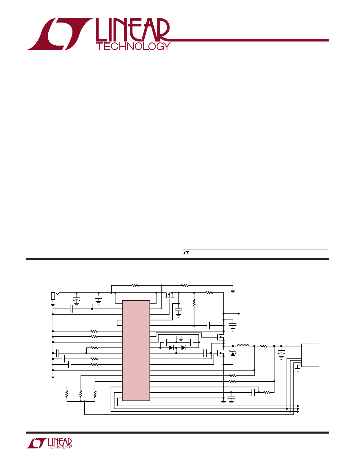
TYPICAL APPLICATIO
ADAPTER
INPUT
AC
0.1µF
1µF
0.33µF
V
DD
475k
+
0.68µF
10µF
35V
Al
10k
0.1µF
V
DD
33k
33k
3.83k
1.5k
1k
1k
U
15.8k
LTC1759
7
UV
16
V
DD
4
SYNC
5
SDB
12
CHGEN
25
V
LIMIT
24
I
LIMIT
18
DGND
17
I
SET
28
PROG
27
V
C
11
COMP1
6
AGND
20
RNR
19
THERM
14
SDA
15
SCL
13
INTB
DCIN
DCDIV
INFET
V
CLP
CLN
TGATE
BOOSTC
GBIAS
BOOST
BGATE
SPIN
SENSE
BAT1
BAT2
V
PGND
22
21
8
32
CC
9
10
2
2.2µF
33
34
1
3
SW
35
30
29
31
23
26
SET
36
Figure 1. 4A SMBus Smart Battery Charger
1k
499Ω
0.47µF
0.1µF
0.68µF
0.033Ω
1µF
SYSTEM
POWER
22µF
15µH
200Ω
200Ω
0.047µF
0.015µF
0.025Ω
68Ω
+
22µF
INTB
SCL
SDA
SMART
BATTERY
SMBus
TO
HOST
1759 F01
1
Page 2
LTC1759
WW
W
U
ABSOLUTE MAXIMUM RATINGS
(Note 1)
Voltage at VCC, UV, BAT1, CLP,CLN, SPIN,
SENSE with respect to AGND ....................–0.3V to 27V
Voltage at DCIN, BAT2 with Respect
to DGND ....................................................–0.3V to 27V
Voltage at INTB, SDA, SCL, DCDIV with Respect
to DGND ..................................................... – 0.3V to 7V
BOOST, BOOSTC Voltage with Respect to VCC........ 10V
Voltage at VDD with Respect to DGND ........ –0.3V to 7V
SW Voltage with Respect to AGND .............. –2V to V
GBIAS, SYNC ............................................ – 0.3V to 10V
VC, PROG, V
Voltage with Respect
SET
to AGND ......................................................– 0.3V to 7V
TGATE, BGATE Current Continuous .................. ±200mA
TGATE, BGATE Output Energy (per Cycle) ................ 2µJ
PGND, DGND with Respect to AGND .................... ±0.3V
Current into Any Pin ......................................... ±100mA
Operating Ambient Temperature Range...... 0°C to 70°C
Operating Junction
Temperature Range .............................. – 40°C to 125°C
Storage Temperature ........................... –65°C to 150°C
Lead Temperature (Soldering, 10 sec)................. 300°C
CC
U
W
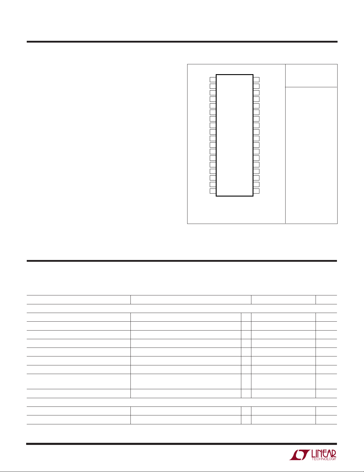
PACKAGE/ORDER INFORMATION
TOP VIEW
1
BOOST
2
TGATE
3
SW
4
SYNC
5
SDB
6
AGND
7
UV
8
INFET
9
CLP
10
CLN
11
COMP1
12
CHGEN
13
INTB
14
SDA
15
SCL
16
V
DD
17
I
SET
18
DGND
G PACKAGE
36-LEAD PLASTIC SSOP
T
= 125°C, θJA = 85°C/W
JMAX
Consult factory for Industrial and Military grade parts.
36
35
34
33
32
31
30
29
28
27
26
25
24
23
22
21
20
19
PGND
BGATE
GBIAS
BOOSTC
V
CC
BAT1
SPIN
SENSE
PROG
V
C
V
SET
V
LIMIT
I
LIMIT
BAT2
DCIN
DCDIV
RNR
THERM
ORDER PART
NUMBER
LTC1759CG
U
ELECTRICAL CHARACTERISTICS
The ● denotes specifications which apply over the full operating temperature range (TJ = 0°C to 100°C), otherwise specifications are
T
= 25°C. V
A
PARAMETER CONDITIONS MIN TYP MAX UNITS
Supply and Reference
DCIN, VCC Operating Voltage ● 11 24 V
VCC Operating Current VCC ≤ 24V ● 12 20 mA
DCIN Operating Current V
UV Lockout Threshold Voltage on UV Pin Rising ● 6.3 6.7 7.15 V
UV Pin Input Current 0V ≤ VUV ≤ 8V ● –1 5 µA
Battery Discharge Current VUV ≤ 0.4V, All Connected Pins 40 80 µA
VDD Operating Voltage ● 3.0 5.5 V
VDD Operating Current Charging, VDD = 5.5V, Shorted Thermistor 1.35 2 mA
VDD Undervoltage Lockout ● 1.6 2.2 2.9 V
Switching Regulator
Charging Voltage Accuracy (Notes 3, 5) 2.465V ≤ V
Charging Current Accuracy (Note 3) R
= DCIN = 18V, V
CC
= 12.6V, VDD = 3.3V unless otherwise specified.
BAT1, 2
= 24V ● 85 150 µA
DCIN
Not Charging, V
Tolerance = 1% –5 5 %
SET
= 5.5V 80 150 µA
DD
≤ V
BAT2
MAX
● –1 1 %
2
Page 3
LTC1759
ELECTRICAL CHARACTERISTICS
The ● denotes specifications which apply over the full operating temperature range (TJ = 0°C to 100°C), otherwise specifications are
T
= 25°C. V
A
PARAMETER CONDITIONS MIN TYP MAX UNITS
BOOST Pin Current V
V
Threshold to Turn T
BOOST
(Note 6) Low to High
BOOSTC Pin Current V
Sense Amplifier CA1 Gain and Input Offset Voltage 11V ≤ VCC ≤ 24V, 0V ≤ V
(With R
(Measured Across R
CA1 Bias Current (SENSE, BAT1) V
CA1 Input Common Mode Range ● –0.25 VCC – 0.3 V
SPIN Input Current V
CL1 Turn-On Threshold 0.5mA Output Current 87 92 97 mV
CL1 Transconductance Output Current from 50µA to 500µA 0.5 1 3 mho
CLP Input Current 0.5mA Output Current 1 3 µA
CLN Input Current 0.5mA Output Current 0.8 2 mA
CA2 Transconductance VC = 1V, IVC = ±1µA 150 200 300 µmho
VA Transconductance (Note 5) Ouput Current from 50µA to 500µA 0.21 0.6 1 mho
Gate Drivers
V
GBIAS
V
High (V
TGATE
V
High I
BGATE
V
Low (V
TGATE
V
Low I
BGATE
INFET “ON” Clamping Voltage (VCC – V
INFET “ON” Drive Current V
INFET “OFF” Clamping Voltage VCC Not Connected, I
INFET “OFF” Drive Current VCC = 12.4V, (VCC – V
V
, V
TGATE
Trip Points
DCDIV Threshold V
DCDIV Hysteresis 25 mV
DCDIV Input Bias Current V
Power-Fail Indicator (V
Power-Fail Indicator Hysteresis (V
SYNC Pin Threshold 0.9 1.4 2.0 V
SYNC Pin Input Current V
= DCIN = 18V, V
CC
= 12.6V, VDD = 3.3V unless otherwise specified.
BAT1, 2
= VSW + 8V, 0V ≤ VSW ≤ 20V
BOOST
TGATE High 2 3 mA
TGATE Low 2 3 mA
Off Measured at (V
GATE
BOOST
– VSW)
Hysteresis 0.25 V
= VCC + 8V 1 mA
BOOSTC
= RS3 = 200Ω)R
S2
TGAGE
TGATE
at Shutdown V
BGATE
) (Note 4) R
S1
– VSW)I
– VSW)I
) ● 6.5 7.8 9 V
INFET
≥ V
BAT2
) (Note 7) AC_PRESENT = 1, V
DCIN
≥ V
BAT2
) AC_PRESENT = 1, V
DCIN
= 4.93k ● 92 100 108 mV
SET
= 49.3k 7 10 13 mV
SET
= High ● –50 –120 µA
SDB
= Low (Shutdown) –10 µA
V
SDB
= High, V
SDB
= Low 10 µA
V
SDB
VCC ≥ 11V, I
TGATE
BGATE
TGATE
BGATE
INFET
= Low, I
SDB
DCDIV
DCDIV
SYNC
V
SYNC
SPIN
GBIAS
≤ 20mA ● 5.6 6.6 V
≤ 20mA ● 6.2 7.2 V
≤ 50mA ● 0.8 V
≤ 50mA ● 0.8 V
= VCC – 6V ● 820 mA
TGATE
Rising from 0.8V to 1.2V ● 0.9 1.0 1.1 V
= 1V ● 100 nA
= 0V –500 µA
= 2V –30 µA
BAT
= 12.6V ● 2mA
≤ 15mA, V
< –2µA 1.4 V
INFET
INFET
= I
BGATE
= 6V ● 0.84 0.89 0.94 V/V
DCIN
= 6V 0.02 V/V
DCIN
● 6.8 7.1 7.3 V
≤ 20V
= High ● 8.4 8.9 9.3 V
SDB
) ≥ 2V –2.5 mA
= 10µA ● 1V
3
Page 4
LTC1759
ELECTRICAL CHARACTERISTICS
The ● denotes specifications which apply over the full operating temperature range (TJ = 0°C to 100°C), otherwise specifications are
T
= 25°C. V
A
PARAMETER CONDITIONS MIN TYP MAX UNITS
Thermistor Decoder (Note 11)
Combined Input Leakage on RNR and THERM 200 nA
Thermistor Trip (COLD/OR) R
Thermistor Trip (IDEAL/COLD) RNR = 10k ±1% ● 26.4 30 33.6 kΩ
Thermistor Trip (HOT/IDEAL) RNR = 10k ±1% ● 2.64 3 3.36 kΩ
Thermistor Trip (UR/HOT) RUR = 1k ±1% ● 440 500 560 Ω
DACs
Charging Current Resolution Guaranteed Monotonic Above I
Charging Current Granularity R
Wake-Up Charging Current (I
Charging Current Limit (I
I
SET RDS(ON)
I
SET IOFF
Charging Voltage Resolution Guaranteed Monotonic (2.5V ≤ V
Charging Voltage Granularity R
Charging Voltage Limit R
Logic Levels (Note 12)
SCL/SDA Input Low Voltage (VIL) ● 0.6 V
SCL/SDA Input High Voltage (VIH) ● 1.4 V
SDA Output Low Voltage (VOL)I
SCL/SDA Input Current (IIL)V
SCL/SDA Input Current (IIH)V
INTB Output Low Voltage (VOL)I
INTB Output Pull-Up Current V
CHGEN Output Low Voltage (VOL)I
CHGEN Output High Voltage (VOH)I
SDB Shutdown Threshold ● 12V
SDB Pin Current 0V ≤ V
Power-On Reset Duration VDD Ramp from 0V to > 3V in < 5µs 100 µs
= DCIN = 18V, V
CC
WAKE-UP
)R
MAX
= 12.6V, VDD = 3.3V unless otherwise specified.
BAT1, 2
= 475k ±1% ● 80 100 120 kΩ
WEAK
/16 10 bits
MAX
= 0 1 mA
ILIMIT
= 10k ±1% 2 mA
R
ILIMIT
R
= 33k ±1% 4 mA
ILIMIT
= Open (or Short to VDD)8mA
R
ILIMIT
) (Note 8) 80 mA
= 0 1023 mA
ILIMIT
= 10k ±1 % 2046 mA
R
ILIMIT
= 33k ±1 % 4092 mA
R
ILIMIT
R
= Open (or Short to VDD) 8184 mA
ILIMIT
25 Ω
V
= 2.7V ● 1 µA
ISET
≤ 21V) 10 bits
BAT
= 0 16 mV
VLIMIT
R
= 10k ±1% 16 mV
VLIMIT
= 33k ±1% 32 mV
R
VLIMIT
= 100k ±1% 32 mV
R
VLIMIT
R
= Open (or Short to VDD)32mV
VLIMIT
= 0 ● 8.33 8.432 8.485 V
VLIMIT
= 10k ±1% ● 12.50 12.64 12.72 V
R
VLIMIT
= 33k ±1% ● 16.67 16.864 16.97 V
R
VLIMIT
R
= 100k ±1% ● 20.82 21.056 21.18 V
VLIMIT
= Open (or Short to VDD) (Note 2) 32.736 V
R
VLIMIT
= 350µA ● 0.4 V
PULLUP
, V
SDA
SDA
PULLUP
INTB
OL
OH
= V
SCL
IL
, V
= V
SCL
IH
= 500µA ● 0.4 V
= V
OL
= 200µA ● 0.4 V
= –200µA ● VDD – 0.4 V
≤ 3V 8 µA
SDB
● 1 µA
● 1 µA
● 3.5 10 17.5 µA
4
Page 5
LTC1759
ELECTRICAL CHARACTERISTICS
The ● denotes specifications which apply over the full operating temperature range (TJ = 0°C to 100°C), otherwise specifications are
T
= 25°C. V
A
PARAMETER CONDITIONS MIN TYP MAX UNITS
Charger Timing
V
, V
TGATE
TGATE, BGATE Peak Drive Current 10nF Load 1 A
Regulator Switching Frequency ● 170 200 230 kHz
Synchronization Frequency ● 240 280 kHz
Maximum Duty Cycle in Start-Up Mode (Note 9) ● 85 90 %
t
TIMEOUT
Cold or Underrange Battery
SMBus Timing (refer to System Management Bus Specification, Revision 1.0, section 2.1 for timing diagrams) (Note 12)
SCL Serial Clock High Period (t
SCL Serial Clock Low Period (t
SDA/SCL Rise Time (tr)C
SDA/SCL Fall Time (tf) ● 30 300 ns
SMBus Accelerator Boosted Pull-Up Current VDD = 3V ● 1 2.5 mA
Start Condition Setup Time (t
Start Condition Hold Time (t
SDA to SCL Rising-Edge Setup Time (t
SDA to SCL Falling-Edge Hold Time, ● 300 ns
Slave Clocking in Data (t
t
TIMEOUT
ChargingCurrent() and ChargingVoltage()
Commands (Note 10)
Note 1: Absolute Maximum Ratings are those values beyond which the life
of a device may be impaired.
Note 2: This limit is greater than the absolute maximum for the charger.
Therefore, there is no effective limitation on voltage when this option is
selected. If the charger is requested to charge with a higher voltage than
the nominal limit, the VOLTAGE_OR bit will be set.
Note 3: Total system accuracy from SMBus request to output voltage or
output current.
Note 4: Test Circuit #1.
Note 5: Voltage accuracy is calculated using measured reference voltage,
obtained from V
ratio.
Note 6: When supply and battery voltage differential is low, high oscillator
duty cycle is required. The LTC1759 has a unique design to achieve duty
cycle greater than 99% by skipping cycles. Only when V
the comparator threshold, will TGATE be turned off. See Applications
Information section.
= DCIN = 18V, V
CC
Rise/Fall Time 1nF Load 25 ns
BGATE
for Wake-Up Charging a ● 140 175 210 sec
HIGH
LOW
SU:STA
HD:STA
)
HD:DAT
Between Receiving Valid ● 140 175 210 sec
pin using Test Circuit #2, and VDAC resistor divider
SET
= 12.6V, VDD = 3.3V unless otherwise specified.
BAT1, 2
)I
)I
) ● 4.7 µs
) ● 4.0 µs
) ● 250 ns
SU:DAT
= 350µA, C
PULLUP
= 350µA, C
PULLUP
= 150pF ● 1000 ns
LOAD
drops below
BOOST
= 150pF ● 4 µs
LOAD
= 150pF ● 4.7 µs
LOAD
Note 7: Power failure bit is set when the battery voltage is above 89% of
the power adapter voltage (V
Note 8: The charger provides wake-up current when a battery is inserted
into the connector, prior to the battery requesting charging current and
voltage. See Smart Battery Charger Specification (Revision 1.0), section
6.1.3 and 6.1.8.
Note 9: In system start-up, C6 (boost capacitor) has no charge stored in it.
The LTC1759 will keep TGATE off, and turn BGATE on for 0.2µs, thus
charging C6. A comparator senses V
PWM mode when V
Note 10: Refer to Smart Battery Charge Specification (Revision 1.0),
section 6.1.2.
Note 11: Maximum total external capacitance on RNR and THERM pins
is 75pF.
Note 12: SMBus operation guaranteed by design from –40°C to 85°C.
BOOST
).
DCIN
and switches to the normal
is above its threshold.
BOOST
5
Page 6
LTC1759
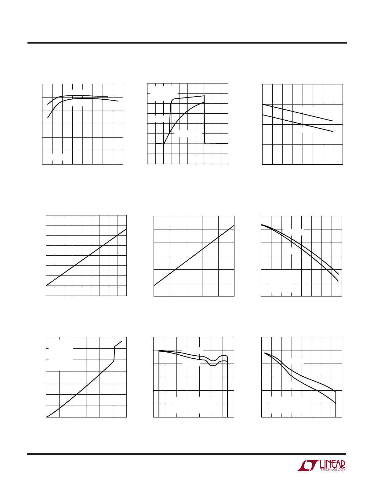
TEMPERATURE (°C)
0
DCDIV (V)
1.10
1.05
1.00
0.95
0.90
1759 G03
10 20 30 40 50 60 70 80
VDD = 5.5V
VDD = 3V
CHARGING CURRENT (mA)
256
1256 2256 3256 4256
OUTPUT CURRENT ERROR (mA)
1759 G06
0
–10
–20
–30
–40
–50
–60
R
ILIMIT
= 33k
V
IN
= 15V
V
OUT
= 12V
T
A
= 25°C
VDD = 5.5V
VDD = 3V
UW
TYPICAL PERFOR A CE CHARACTERISTICS
Charger Efficiency
100
95
90
85
EFFICIENCY (%)
80
75
VIN = 20V
70
0.5
16.8V
12.6V
1.5 2.5 3.5
CHARGING CURRENT (A)
Current from Battery vs Battery
Voltage (Does Not Include V
Current)
90
TA = 25°C
80
70
60
(µA)
50
BAT
I
40
30
20
10
6 8 10 12 14 16 18 20 22 24
V
(V)
BAT
1759 G09
DD
1759 G04
SMBus Accelerator Operation DCDIV Trip Point vs Temperature
VCC = 5V
5V
= 200pF
C
LD
= 25°C
T
A
LTC1759
R
= 15k
PULLUP
0V
1µs/DIV
1759 G02
IDD vs VDD (Not Charging) Programmed Current Accuracy
120
TA = 25°C
110
100
90
(µA)
DD
I
80
70
60
3.0 3.5 4.0 4.5 5.0 5.5
VDD (V)
1759 G05
Low Current Mode
350
R
ILIMIT
= 15V
V
IN
300
V
OUT
= 25°C
T
A
250
C
PROG
R
SET
200
150
100
OUTPUT CURRENT (mA)
50
0
0
6
= 33k
= 12V
= 1nF
= 3.83k
50 100 150 200 250 300
CHARGING CURRENT (mA)
1759 G01
0
–5
–10
–15
–20
OUTPUT VOLTAGE ERROR (mV)
–25
–30
2000 3000 4000 5000 6000 7000 8000 9000
VDD = 5.5V
VDD = 3V
R
= 0
VLIMIT
LOAD CURRENT = 15mA
T
= 25°C
A
CHARGING VOLTAGE (mV)
1759 G07
Charging Voltage ErrorCharging Voltage Error
0
–5
–10
–15
–20
OUTPUT VOLTAGE ERROR (mV)
–25
–30
2000
VDD = 5.5V
VDD = 3V
R
= 33k
VLIMIT
LOAD CURRENT = 15mA
T
= 25°C
A
6000 10000 14000 18000
CHARGING VOLTAGE (mV)
1759 G08
Page 7

UUU
PIN FUNCTIONS
LTC1759
Input Power-Related Pins
UV (Pin 7): Charger Section Undervoltage Lockout Pin.
The rising threshold is 6.7V with a hysteresis of 0.5V.
Switching stops in undervoltage lockout. Connect this
input to the input voltage source with no resistor divider.
UV must be pulled below 0.7V when there is no input
voltage source (5k resistor from adapter output to ground
is required) to obtain the lowest quiescent battery current.
INFET (Pin 8): Gate Drive to Input P-channel FET. For very
low dropout applications, use an external P-channel FET to
connect the adapter output and VCC. INFET is clamped to
7.8V below VCC.
CLP (Pin 9): Positive Input to the Input Current Limit
Amplifier CL1. When used to limit supply current, a filter
(R3 and C1 of Figure 10) is needed to filter out the
switching noise. The threshold is set at 92mV.
CLN (Pin 10): Negative Input to the Input Current Limit
Amplifier CL1. It should be connected to VCC (to the V
bypass capacitor C2 for less noise).
COMP1 (Pin 11): Compensation Node for the Input Current Limit Amplifier CL1. At input adapter current limit, this
node rises to 1V. By forcing COMP1 low with an external
transistor, amplifier CL1 will be defeated (no adapter
current limit). COMP1 can source 200µA. Ground (to
AGND) this pin if the adapter current limiting function is
not used.
CC
Battery Charging-Related Pins
BOOST (Pin 1): This pin is used to bootstrap and supply
power for the topside power switch gate drive and control
circuity. In normal operation, V
internally generated 8.6V regulator V
+ 8.9V when TGATE is high. Do not force an external
voltage on BOOST pin.
TGATE (Pin 2): This pin provides gate drive to the topside
power FET. When TGATE is driven on, the gate voltage will
be approximately equal to VSW + 6.6V. A series resistor of
5Ω to 10Ω should be used from this pin to the gate of the
topside FET.
is powered from an
BOOST
, V
GBIAS
BOOST
≈ V
CC
SW (Pin 3): This pin is the reference point for the floating
topside gate drive circuitry. It is the common connection
for the top and bottom side switches and the output
inductor. This pin switches between ground and VCC with
very high dv/dt rates. Care needs to be taken in the PC
layout to keep this node from coupling to other sensitive
nodes. A 1A Schottky clamping diode should be placed
very close to the chip from the ground pin to this pin to
prevent the chip substrate diode from turning on. See
Applications Information for more details.
SYNC (Pin 4): External Clock Synchronization Input. Pulse
width range: 10% to 90%.
SDB (Shutdown Bar) (Pin 5): Active Low Digital Input. The
charger is disabled when asserted. This pin is connected
to the CHGEN pin to enable charger control through the
SMBus interface.
CHGEN (Pin 12): Digital Output to Enable Charger Function. Connect CHGEN to SDB.
I
(Pin 17): Open-Drain CMOS Switch to DGND. An
SET
external resistor, R
current programming input, the PROG pin of the battery
charger section, which sets the range of the charging
current.
I
(Pin 24): An external resistor is connected between
LIMIT
this pin and DGND. The value of the external resistor
programs the range and resolution of the programmed
charger current. See Electrical Characteristics table for
more information.
V
(Pin 25): An external resistor is connected between
LIMIT
this pin and DGND. The value of the external resistor
programs the range and resolution of the V
Electrical Characteristics table for more information.
V
(Pin 26): This is the tap point of the programmable
SET
resistor divider, which provides battery voltage feedback
to the charger.
, is connected from I
SET
SET
divider. See
SET
to the
7
Page 8

LTC1759
UUU
PIN FUNCTIONS
VC (Pin 27): This is the control signal of the inner loop of
the current mode PWM. Switching starts at 0.9V. Higher
VC corresponds to higher charging current in normal
operation. A capacitor of at least 0.33µF to AGND filters out
noise and controls the rate of soft start.
PROG (Pin 28): This pin is for programming the charging
current and for system loop compensation. During normal
operation, the pin voltage is approximately 2.465V.
SENSE (Pin 29): Current Amplifier CA1 Input. Sensing
must be at the positive terminal of the battery.
SPIN (Pin 30): This pin is for the internal amplifier
CA1 bias. It must be connected to R
Figure 1.
BAT1 (Pin 31): Current Amplifier CA1 Input.
BOOSTC (Pin 33): This pin is used to bootstrap and supply
the current sense amplifier CA1 for very low dropout
conditions. VCC can be as low as only 0.4V above the
battery voltage. A diode and a capacitor are needed to get
the voltage from V
VCC is always 3V or greater than V
floating or tied to VCC. Do not force this pin to a voltage
lower than VCC.
BGATE (Pin 35): Drives the gate of the bottom external
N-channel FET of the charger buck converter.
. If low dropout is not needed and
BOOST
BAT
as shown in
SENSE
, this pin can be left
Internal Power Supply Pins
AGND (Pin 6): DC Accurate Ground for Analog Circuitry.
VDD (Pin 16): Low Voltage Power Supply Input. Bypass
this pin with 0.1µF.
DGND (Pin 18): Ground for Digital Circuitry and DACs.
Should be connected to AGND at the negative terminal
of the charger output filter capacitor.
VCC (Pin 32): Power Input for Battery Charger Section.
Bypass this pin with 0.47µF.
GBIAS (Pin 34): 8.6V Regulator Output for Bootstrapping
V
needed. Switching will stop if V
PGND (Pin 36): High Current Ground Return for Charger
Gate Drivers.
SBS Interface Pins
INTB (Interrupt Bar) (Pin 13): Active Low Interrupt Output
to Host. Signals host that there has been a change of status
in the charger registers and that the host should read the
LTC1759 status registers to determine if any action on its
part is required. This signal can be connected to the
optional SMBALERT# line of the SMBus. Open drain with
weak current source pull-up to VDD (with Schottky to allow
it to be pulled to 5V externally, see Figure 2).
BOOST
and V
BOOSTC
. A bypass capacitor of at least 2µF is
drops below 7.1V.
BOOST
Monitor/Fault Diagnostic Pins
DCDIV (Pin 21): Supply Divider Input. This is a high
impedance comparator input with a 1V threshold (rising
edge) and hysteresis.
DCIN (Pin 22): Input connected to the DC input source to
monitor the DC input for power-fail condition.
BAT2 (Pin 23): Sensing Point for Voltage Control Loop.
Connect this to the positive terminal of the battery.
8
SDA (Pin 14): SMBus Data Signal from Main (Hostcontrolled) SMBus.
SCL (Pin 15): SMBus Clock Signal from Main (HostControlled) SMBus. External pull-up resistor is required.
THERM (Pin 19): Thermistor Force/Sense Pin to Smart
Battery. See Electrical Characteristics table for more
detail. Maximum allowed combined capacitance on THERM
and RNR is 75pF.
RNR (Pin 20): Thermistor Force/Sense Pin to Smart
Battery. See Electrical Characteristics table for more
detail. Maximum allowed combined capacitance on THERM
and RNR is 75pF.
Page 9
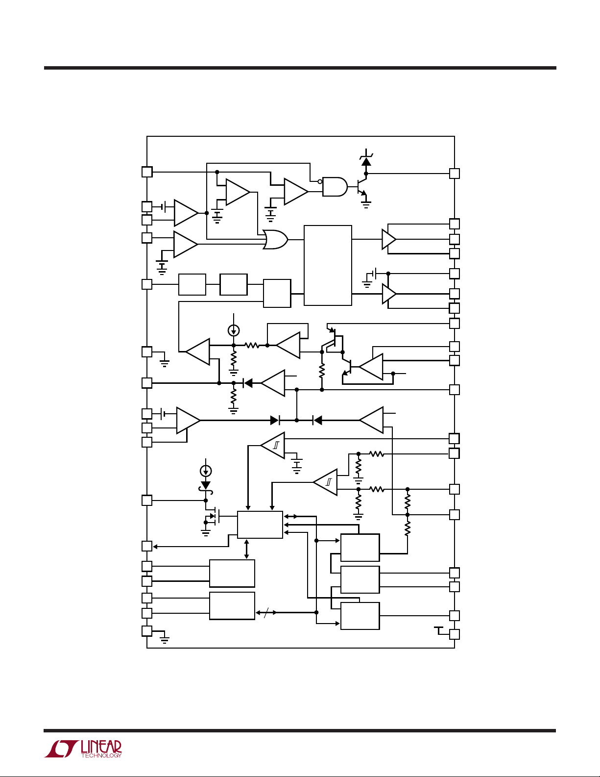
BLOCK DIAGRA
7
UV
0.2V
31
BAT1
32
V
CC
5
SDB
4
SYNC
6
AGND
V
27
C
92mV
+
CLP
9
CLN
10
COMP1
11
INTB
13
CHGEN
12
THERM
19
20
RNR
SCL
15
SDA
14
DGND
18
W
1.3V
LTC1759
V
CC
8V
8
INFET
1
BOOST
TGATE
2
3
SW
GBIAS
34
35 BGATE
36
PGND
33
BOOSTC
30
SPIN
29
SENSE
28
PROG
21
DCDIV
22
DCIN
23
BAT2
V
26
SET
I
24
LIMIT
25
V
LIMIT
17
I
SET
V
16
DD
1759 F02
S
R
CA2
13
+
–
6.7V
Q
–
B1
+
–
+
–
PWR_FAIL
+
V
SHDN
REF
1V
PWM
LOGIC
1k
–
+
20k
65k
10-BIT
VOLTAGE
DAC
LIMIT
DECODER
10-BIT
CURRENT
DAC
8.9V
CA1
VA
290k
812.5k
+
–
–
BAT1
V
REF
+
612k
72k
+
SLOPE COMP
+
–
V
DD
10µA
THERMISTOR
DECODER
CONTROLLER
–
6.7V
200kHz
OSC
75k
AC_PRESENT
CHARGER
CONTROLLER
SMBus
+
–
–
+
ONE
SHOT
C1
+
CL1
–
Figure 2
9
Page 10

LTC1759
TEST CIRCUITS
Test Circuit 1
SPIN
SENSE
BAT1
R
S3
200Ω
R
S2
200Ω
R
SENSE
10Ω
+
V
BAT
V
0.047µF
LTC1759
–
C
75k
CA2
+
V
REF
300Ω
1µF
1k
PROG
R
SET
+
CA1
–
+
1k
+
≈ 0.65V
LT1006
–
1759 TC01
20k
Test Circuit 2
10
I
0.47µF
PROG
LTC1759
V
SET
+
VA
V
–
REF
PROG
2k
R
SET
+
2.465V
–
LT1013
+
2nF
1759 TC02
Page 11

OPERATIO
LTC1759
U
Overview (Refer to Block Diagram and Figure 10)
The LTC1759 is composed of a battery charger section, a
charger controller, two 10-bit DACs to control charger
parameters, a thermistor decoder, limit decoder and an
SMBus controller block. If no battery is present, the
thermistor decoder indicates a THERM_OR condition and
charging is disabled by the charger controller (CHGEN =
Low). Charging will also be disabled if AC_PRESENT is
low, or the battery thermistor is decoded as THERM_HOT.
If a battery is inserted or AC power is connected, the
battery will be charged with an 80mA “wake-up” current.
The wake-up current is discontinued after three minutes
if the thermistor is decoded as THERM_UR or
THERM_COLD, and the battery or host doesn’t transmit
charging commands.
The SMBus controller block receives ChargingCurrent()
and ChargingVoltage() commands via the SMBus. If
ChargingCurrent() and ChargingVoltage() command pairs
are received within a three-minute interval, the values are
stored in the current and voltage DACs and the charger
controller asserts the CHGEN line if the decoded thermistor value will allow charging to commence.
ChargingCurrent () and ChargingVoltage() values are compared against limits programmed by the limit decoder
block; if the commands exceed the programmed limits
these limits are substituted and overrange flags are set.
The charger controller will assert INTB whenever a status
change is detected. The host may query the charger, via
the SMBus, to obtain ChargerStatus() information. INTB
will be deasserted upon a successful read of
ChargerStatus() or a successful Alert Response Address
(ARA) request.
accuracy is achieved with averaging capacitor C
Note that I
generates a ramp signal that is fed to the PWM control
comparator C1 through buffer B1 and level shift resistors
forming the current mode inner loop. The BOOST pin
supplies the top power switch gate drive. The LTC1759
generates a 8.9V V
V
BOOSTC pin supplies the current amplifier CA1 with a
voltage higher than VCC for low dropout applications.
Amplifier VA reduces the charging current when the battery voltage reaches the set voltage programmed by the
VDAC and the 2.465V reference voltage.
The amplifier CL1 monitors and limits the input current,
normally from the AC adapter, to a preset level (92mV/
RCL). At input current limit, CL1 will supply the programming current I
current.
The INFET pin drives an external input P-channel FET for
low dropout applications.
SMBus Interface
All communications over the SMBus are interpreted by the
SMBus controller block. The SMBus controller is an
SMBus slave device. All internal LTC1759 registers may
be updated and accessed through the SMBus controller,
and charger controller as required. The SMBus protocol is
a derivative of the I2CTM bus (Reference
as well as to drive the bottom power FET. The
BOOSTC
to Use It, V1.0”
Specification”
tion*, for a complete description of the bus protocol
requirements.)
has both AC and DC components. I
PROG
for bootstrapping V
GBIAS
and thus reduce battery charging
PROG
BOOST
“I2C-Bus and How
by Philips and
by the Smart Battery System Organiza-
“System Management Bus
PROG
PROG
and
.
Battery Charger Section
The LTC1759 is synchronous current mode PWM stepdown (Buck) switcher. The battery DC charging current is
programmed with a current DAC via the SMBus interface.
Amplifier CA1 converts the charging current through
R
R
pares the output of CA1 with the programmed current and
drives the PWM loop to force them to be equal. High DC
to a much lower current I
SENSE
SENSE/RS2
) fed into the PROG pin. Amplifier CA2 com-
PROG (IPROG
= I
BAT
•
All data is clocked into the shift register on the rising edge
of SCL. All data is clocked out of the shift register on the
falling edge of SCL. Detection of an SMBus Stop condition,
or power-on reset via the VDD undervoltage lockout, will
reset the controller to an initial state at any time.
The LTC1759 command set is interpreted by the SMBus
controller and passed onto the charger controller block as
control signals or updates to internal registers.
I2C is a trademark of Philips Electronics N.V.
*http://www. SBS-FORUM.org
11
Page 12

LTC1759
U
OPERATIO
Table 1: Supported Charger Functions
SMBus ADDRESS COMMAND CODE
FUNCTION (7-BIT) (8-BIT hex) ACCESS DATA TYPE
ChargerSpecInfo() b0001_001 h11 r Register
ChargerMode() b0001_001 h12 w Register
ChargerStatus() b0001_001 h13 r Register
ChargingCurrent() b0001_001 h14 w Register
ChargingVoltage() b0001_001 h15 w Register
AlarmWarning() b0001_001 h16 w Control
LTCVersionFunction() b0001_001 h3c r Register
OptionalMfgFunction3() b0001_001 h3d – Not Supported
OptionalMfgFunction2() b0001_001 h3e – Not Supported
OptionalMfgFunction1() b0001_001 h3f – Not Supported
Alert Response Address
1
Read-byte format. 89h is returned as the interrupt address of the LTC1759. Rev 1.0 SMBus Compliant.
Table 2: SMBus Word Bit Definitions for All Allowed LTC1759 Functions
FUNCTION FIELD MAPPING (BINARY) ALLOWED VALUES
ChargerSpecInfo CHARGER_SPEC 3:0 0001 • The CHARGER_SPEC Reports the Version of the Smart Battery
ChargerMode() INHIBIT_CHARGE 0 0 • 0 – Enable Charging (Power-On Default)
1
SELECTOR_SUPPORT 4 0 • 0 – Charger Does Not Support the Optional Smart Battery Selector
Reserved 15:5 0 • These Bits Are Reserved and Must Return Zero
ENABLE_POLLING 1 0 • 0 – Disable Polling (Power-On Default for Smart Battery Controlled
b0001_100 N/A Read Byte Interrupt Address
POWER-ON
WORD BIT RESET VALUE
Charger Specification the Charger Supports
• 0001 – Version 1.0
• All Other Codes Reserved
• Always Returns 0001
• Read Only. Write Will NACK
Commands
• 1 – Charger Supports the Optional Smart Battery Selector
Commands
• Always Returns 0
• Read Only. Write Will NACK
• Read Only. Write Will NACK
• 1 – Inhibit Charging
• Write Only. Read Will NACK
• Cleared to Power-On Reset Value When:
1) POR_RESET = 1
2) AC_PRESENT = 0
3) BATTERY_PRESENT = 0
Chargers)
• 1 – Enable Polling (Power-On Default for Host Controlled Chargers).
• Ignored by LTC1759
• Write Only. Read Will NACK
12
POR_RESET 2 0 • 0 – Mode Unchanged (Default)
• 1 – Set Charger to Power-On Defaults
• This Reset Only Affects the Charger_Controller Block
• Write Only. Read Will NACK
Page 13

U
OPERATIO
POWER-ON
WORD BIT RESET VALUE
FUNCTION FIELD MAPPING (BINARY) ALLOWED VALUES
RESET_TO_ZERO 3 0 • 0 – Charging Value Unchanged
• 1 – Set Charging Values to Zero
NOTE:
This function is implemented by forcing the charger to
CHARGING_NONE_STATE and not allowing charge to resume until a
valid ChargingCurrent() and ChargingVoltage() Pair Is received.
• Write Only. Read Will NACK
Reserved 15:4 0 • Not Implemented. Writes to These Bits Are Ignored.
• Write Only. Read Will NACK
ChargerStatus() CHARGE_INHIBITED 0 0 This Is the ChargerMode() INHIBIT_CHARGE Bit
• 0 – Charger Is Enabled
• 1 – Charger Is Inhibited
• Read Only. Write Will NACK
MASTER_MODE 1 0 • 0 – Charger Is in Slave Mode (Polling Disabled)
• 1 – Charger Is in Master Mode (Polling Enabled)
• Always Returns 0
• Read Only. Write Will NACK
VOLTAGE_NOTREG 2 0 • 0 – Charger’s Output Voltage Is in Regulation
• 1 – Requested ChargingCurrent() Is Not Being Met
• Not Supported; Always Returns 0
• Read Only. Write Will NACK
CURRENT_NOTREG 3 0 • 0 – Charger’s Output Current Is in Regulation
• 1 – Requested ChargingCurrent() Is Not Being Met
• Not Supported; Always Returns 0
• Read Only. Write Will NACK
LEVEL_3:LEVEL_2 5:4 01 • 00 – Reserved
• 01 – Charger Is a Smart Battery Controlled
• 10 – Reserved
• 11 – Charger Is a Host Controlled
• Always Returns 01
• Read Only. Write Will NACK
CURRENT_OR 6 0 • 0 – ChargingCurrent() Value Is Valid
• 1 – ChargingCurrent() Value Is Invalid
• This Value Is Valid Only When Charging with
CHARGE_INHIBITED = 0 or 1
• Read Only. Write Will NACK
VOLTAGE_OR 7 0 • 0 – ChargingVoltage() Value Is Valid
• 1 – ChargingVoltage() Value Is Invalid
• This Value Is Valid Only When Charging with
CHARGE_INHIBITED = 0 or 1
• Read Only. Write Will NACK
THERM_OR 8 Value • 0 – Thermistor Indicates Not Overrange
• 1 – Thermistor Indicates Overrange
• Read Only. Write Will NACK
THERM_COLD 9 Value • 0 – Thermistor Indicates Not Cold
• 1 – Thermistor Indicates Cold
• Read Only. Write Will NACK
THERM_HOT 10 Value • 0 – Thermistor Indicates Not Hot
• 1 – Thermistor Indicates Hot
• Read Only. Write Will NACK
LTC1759
13
Page 14

LTC1759
U
OPERATIO
POWER-ON
WORD BIT RESET VALUE ALLOWED VALUES
FUNCTION FIELD MAPPING (BINARY)
THERM_UR 11 Value • 0 – Thermistor Indicates Not Underrange
• 1 – Thermistor Indicates Underrange
• Read Only. Write Will NACK
ALARM_INHIBITED 12 0 • 0 – Charger Not Alarm Inhibited
• 1 – Charger Alarm Inhibited. This Bit Is Set but Never Cleared by
AlarmWarning()
• Read Only. Write Will NACK
• Cleared to Power-On Reset Value When:
1) POR_RESET = 1
2) BATTERY_PRESENT = 0
3) AC_PRESENT = 0
4) A Valid ChargingVoltage(), ChargingCurrent() Pair Is Received
POWER_FAIL 13 Value • 0 – V
BATTERY_PRESENT 14 Value • 0 – Battery Is Not Present
AC_PRESENT 15 Value • 0 – Charge Power Is Not Available
ChargingCurrent() CHARGING_CURRENT 15:0 0 • Unsigned Integer Representing Charger Current in mA
[15:0] • Three Possible Responses
ChargingVoltage() CHARGING_VOLTAGE 15:0 0 • Unsigned Integer Representing Charger Voltage in mV
[15:0] • Three Possible Responses
AlarmWarning() OVER_CHARGED_ 15 0 • 1 – Terminate Charging Immediately
ALARM • Write Only. Read Will NACK
TERMINATE_CHARGE_ 14 0 • 1 – Terminate Charging Immediately
ALARM • Write Only. Read Will NACK
RESERVED_ALARM1 13 0 • 1 – Terminate Charging Immediately
OVER_TEMP_ALARM 12 0 • 1 – Terminate Charging Immediately
BAT/VDCIN
• 1 – V
BAT/VDCIN
• Read Only. Write Will NACK
• 1 – Battery Is Present
• Read Only. Write Will NACK
• 1 – Charge Power Is Available
• Read Only. Write Will NACK
– Supply the Current Requested
– Supply Its Programmatic Maximum Current If the Request Is
Greater Than Its Programmatic Value and Less Than hffff
– Supply Its Maximum Safe Current If the Request Is hffff [Supply
Current Required to Meet ChargingVoltage()].
• Write Only. Read Will NACK
– Supply the Voltage Requested
– Supply Its Programmatic Maximum Voltage If the Request Is
Greater Than Its Programmatic Value and Less Than hffff
– Supply Its Maximum Voltage If the Request Is hffff [Supply
Voltage Required to Meet ChargingCurrent()].
• Write Only. Read Will NACK
• Writing a 0 to This Bit Will Be Ignored
• Writing a 0 to This Bit Will Be Ignored.
• Write Only. Read Will NACK
• Writing a 0 to This Bit Will Be Ignored.
• Write Only. Read Will NACK
• Writing a 0 to This Bit Will Be Ignored.
< 0.9
> 0.9
14
Page 15

U
OPERATIO
POWER-ON
WORD BIT RESET VALUE ALLOWED VALUES
FUNCTION FIELD MAPPING (BINARY)
TERMINATE_ 11 0 • This Bit May Be Used to Signal That the Charger May Be Restarted
DISCHARGE_ALARM After a Battery Conditioning Cycle Has Been Completed
• Write Only. Read Will NACK
• Writing a 0 to This Bit Will Be Ignored
• Not Supported by LTC1759
Reserved 10 – • Not Supported by LTC1759
• Write Only. Read Will NACK
REMAINING_ 9 – • Intended for Host
CAPACITY_ALARM • Not Supported by LTC1759
• Write Only. Read Will NACK
REMAINING_TIME_ 8 – • Intended for Host
ALARM • Not Supported by LTC1759
• Write Only. Read Will NACK
INITIALIZED 7 – • Intended for Host
• Not Supported by LTC1759
• Write Only. Read Will NACK
DISCHARGING 6 – • Intended for Host
• Not Supported by LTC1759
• Write Only. Read Will NACK
FULLY_CHARGED 5 – • Intended for Host
• Not Supported by LTC1759
• Write Only. Read Will NACK
FULLY_DISHARGED 4 – • Intended for Host
• Not Supported by LTC1759
• Write Only. Read Will NACK
ERROR 3:0 – • Intended for Host
• All Bits Set High Prior to AlarmWarning() Transmission
• Not Supported by LTC1759
• Write Only. Read Will NACK
LTCVersionFunction LTC_VERSION 15:0 0101hex • Returns LTC Version Number
() • Read Only
• Always Returns 0101hex
LTC1759
SMBus Accelerator Pull-Ups
Both SCL and SDA have SMBus accelerator circuits which
reduce the rise time on systems with significant capacitance on the two SMBus signals. The dynamic pull-up
circuitry detects a rising edge on SDA or SCL and applies
2mA to 5mA pull-up to VDD for approximately 1µs (exter-
nal pull-up resistors are still required to supply DC current). This action allows the bus to meet SMBus rise time
requirements with as much as 150pF on each SMBus
signal. The improved rise time will benefit all of the devices
which use the SMBus, especially those devices that use
the I2C logic levels. Note that the dynamic pull-up circuits
only pull to VDD, so some SMBus devices that are not
compliant to the SMBus specifications may still have rise
time compliance problems if the SMBus pull-up resistors
are terminated with voltages higher than VDD.
15
Page 16

LTC1759
OPERATIO
U
The Charger Controller Block
The LTC1759 charger operations are handled by the
charger controller block. This block is capable of charging
the selected battery autonomously or under host control.
The charger controller can request communications with
the system management host (SMHost) by asserting
INTB = 0; this will cause the SMHost, if present, to poll the
LTC1759.
The charger controller receives SMBus slave commands
from the SMBus controller block.
The charge controller allows the LTC1759 to meet the
following Smart Battery-controlled (Level 2) charger
requirements:
1. Implements the Smart Battery’s critical warning messages over the SMBus.
2. Operates as an SMBus slave device that responds to
ChargingVoltage() and ChargingCurrent() commands
and adjusts the charger output characteristics
accordingly.
The charger controller allows the LTC1759 to meet the
following host-controlled (Level 3) Smart Battery charger
requirements.
1. In a host-controlled system the host is able to operate
as an SMBus master device.
2. The host may determine the appropriate charging algorithm by querying the battery or providing an alternative
special charging algorithm.
3. The host may control charging by disabling the Smart
Battery’s ability to transmit ChargingCurrent() and
ChargingVoltage() request functions and broadcasting
the charging commands to the LTC1759 over the SMBus.
4. The LTC1759 will still respond to Smart Battery critical
warning messages without host intervention.
The charger controller block uses the state machine of
Figure 3. The functional features for state transitions and
general control are detailed in Table 3.
15
0
CHARGING_RESET_STATE
7
1 OR 2
CHARGING_WAKE-UP_STATE
20
3 OR 4 OR 5
OR 6 OR 16
CHARGING_NONE_STATE
NOTE: NUMBERS REFER TO CONDITIONS AND STATE DESCRIPTION IN TABLE 3
Figure 3. Charger Controller State Machine
19
15
8 OR 9
22
15
CHARGING_CONTROLLED_STATE
21
8 OR 9
14
10 OR 11 OR 12
OR 13 OR 16
15
1759 F03
16
Page 17

LTC1759
U
OPERATIO
Table 3. Charger_Controller Functional Features
# CONDITION ACTION
0 POWER_ON_RESET = 1 CHARGING_RESET_STATE =1
(Asynchronously Reset the Charger_Controller State Machine During
Power-On Reset)
1 CHARGING_RESET_STATE = 1 AND the Battery Is Present CHARGING _WAKE-UP_STATE = 1
AND AC_PRESENT = 1 AND INHIBIT_CHARGE = 0 AND Thermistor Is The Charger_Controller Will “Wake Up” Charge the Battery
Ideal at I
2 CHARGING_RESET_STATE = 1 AND the Battery Is Present CHARGING_WAKE-UP_STATE = 1
AND AC_PRESENT =1 AND INHIBIT_CHARGE = 0 AND THERM_ The Charger_Controller Will “Wake Up” Charge the Battery
UR = 1 OR THERM_COLD = 1 at I
3 CHARGING_WAKE-UP_STATE = 1 AND the Time-Out Period CHARGING_NONE_STATE = 1
Exceeds t
4 CHARGING_WAKE-UP_STATE = 1 AND an AlarmWarning() Message CHARGING_NONE_STATE =1
Is Received with Any Bit in the Upper Nibble Set The Charger_Controller Stops Charging the Battery. It Cannot
5 CHARGING_WAKE-UP_STATE = 1 (from Condition 1 above) AND CHARGING_NONE_STATE = 1
THERM_HOT Changes from 0 to 1 AND THERM_UR = 0 The Charger_Controller Stops Charging the Battery. It Cannot
6 CHARGING_WAKE-UP_STATE = 1 (from Condition 2 above) AND CHARGING_NONE_STATE = 1
THERM_UR Changes from 1 to 0 AND THERM_HOT = 1 The Charger_Controller Stops Charging the Battery. It Cannot
7 CHARGING_WAKE-UP-STATE = 1 AND INHIBIT_CHARGE Is CHARGING_WAKE-UP_STATE =1
Set to 1 The Charger_Controller Stops Charging the Selected Battery. The Timer
8 (CHARGING_WAKE-UP_STATE = 1 OR CHARGING_NONE_STATE = 1) CHARGING_CONTROLLED_STATE = 1
AND (Both ChargingCurrent() AND ChargingVoltage() Commands The Charger_Controller Will Supply “Controlled Charge” to the
Are Received within t
AND THERM_HOT = 0
9 (CHARGING_WAKE-UP_STATE = 1 OR CHARGING_NONE_STATE = 1) CHARGING_CONTROLLED_STATE = 1
AND (Both ChargingCurrent() AND ChargingVoltage() Commands The Charger_Controller Will Supply “Controlled Charge” to the
Are Received within t
AND THERM_UR = 1
10 CHARGING_CONTROLLED_STATE = 1 CHARGING_NONE_STATE = 1
AND No New ChargingCurrent() and ChargingVoltage() Commands Are The Charger_Controller Stops Charging the Battery. It Cannot
Received for a Time-Out Period of t
11 CHARGING_CONTROLLED_STATE = 1 CHARGING_NONE_STATE = 1
The Charger_Controller Is Supplying “Controlled Charge” to the The Charger_Controller Stops Charging the Battery. It Cannot
Battery AND (an AlarmWarning() Message Is Received “Wake Up” Charge Again Until Condition 15 Is Met. It Can Supply
with Any Bit in the Upper Nibble Set) “Controlled Charge” to the Battery If Conditions 8 or 9 Are Met
AND THERM_UR = 1 OR THERM_COLD = 1 The Charger_Controller Stops Charging the Battery. It Cannot
TIMEOUT
) AND INHIBIT_CHARGE = 0 Battery as Specified in the Current and Voltage Commands
TIMEOUT
) AND INHIBIT_CHARGE = 0 Battery as Specified in the Current and Voltage Commands
TIMEOUT
TIMEOUT
“Wake Up” Charge Again Until Condition 15 Is Met. It Can Supply
“Controlled Charge” to the Battery If Conditions 8 or 9 Are Met
“Wake Up” Charge Again Until Condition 15 Is Met. It Can Supply
“Controlled Charge” to the Battery If Conditions 8 or 9 Are Met
“Wake Up” Charge Again Until Condition 15 Is Met. It Can Supply
“Controlled Charge” to the Battery If Conditions 8 or 9 Are Met
“Wake Up” Charge Again Until Condition 15 Is Met. It Can Supply
“Controlled Charge” to the Battery If Conditions 8 or 9 Are Met
Continues to Run. The Charger Can Resume “Wake-Up” Charging If
INHIBIT_CHARGE = 0
“Wake Up” Charge Again Until Condition 15 Is Met. It Can Supply
“Controlled Charge” to the Battery If Conditions 8 or 9 Are Met
Indefinitely
WAKE-UP
Until Condition 3 Is Met
WAKE-UP
17
Page 18

LTC1759
U
OPERATIO
# CONDITION ACTION
12 CHARGING_CONTROLLED_STATE = 1 AND THERM_HOT CHARGING_NONE_STATE = 1
Changes from 0 to 1 AND THERM_UR = 0 The Charger_Controller Stops Charging the Battery. It Cannot
“Wake Up” Charge Again Until Condition 15 Is Met. It Can Supply
“Controlled Charge” to the Battery If Conditions 8 or 9 Are Met
13 CHARGING_CONTROLLED_STATE = 1 AND THERM_UR CHARGING_NONE_STATE = 1
Changes from 1 to 0 AND THERM_HOT = 1 The Charger_Controller Stops Charging the Battery. It Cannot
“Wake Up” Charge Again Until Condition 15 Is Met. It Can Supply
“Controlled Charge” to the Battery If Conditions 8 or 9 Are Met
14 CHARGING_CONTROLLED_STATE = 1 CHARGING_CONTROLLED_STATE = 1
AND INHIBIT_CHARGE Is Set to 1 INHIBIT_CHARGE Asynchronously Inhibits Charging Without
Affecting the Charger_Controller State Machine. This Means the Charger
Stops Charging the Battery but Continues to Accept New
ChargingCurrent() and ChargingVoltage() Commands, Continues to
Monitor the Battery Thermistor Input and Continues to Track the
Communication Time-Out. It Will Resume Charging the Battery If
INHIBIT_CHARGE Is Cleared to 0, Possibly at Different Current and
Voltage If New Commands Have Been Sent in the Interim
15 ANY STATE CHARGING_RESET_STATE= 1
The Charger_Controller Is in Any State AND (the Battery Is Removed The Charger_Controller Is Set to Its Power-On Default State
OR AC_PRESENT = 0 OR a 1 Is Written to POR_RESET)
NOTE:
Condition 15 Takes Precedence Over Any Other Condition.
16 (CHARGING_CONTROLLED_STATE = 1) OR CHARGING_NONE_STATE = 1
CHARGING_WAKE-UP_STATE = 1) AND The Charger_Controller Stops Charging the Battery. It Cannot
A 1 Is Written to RESET_TO_ZERO “Wake Up” Charge Again Until Condition 15 Is Met. It Can Supply
“Controlled Charge” to the Battery If Conditions 8 or 9 Are Met.
The Valid Charge Command Timer Is Cleared When RESET_TO_ZERO =
1. This Prevents Charging from Continuing Until After a Valid
ChargeCurrent() and ChargeVoltage() Pair Is Received
18 ANY STATE AND Alert SMHost of Change by Setting INTB = 0
AC_PRESENT Transitions 0 to 1 or 1 to 0 OR
BATTERY_PRESENT Transitions 0 to 1 or 1 to 0
19 CHARGING_RESET_STATE = 1 CHGEN = 0
The Charger Is Not Charging
20 CHARGING _WAKE-UP_STATE = 1 CHGEN = ~INHIBIT_CHARGE
The Charger Will Provide a Wake-Up Current When CHGEN = 1
21 CHARGING_CONTROLLED_STATE = 1 CHGEN = ~INHIBIT_CHARGE
The Charger Will Provide Specified Charging Voltage and Current
When CHGEN = 1
A Zero Value for ChargingVoltage() Is Handled by Forcing CHGEN = 0
22 CHARGING_NONE_STATE = 1 CHGEN = 0
The Charger Is Not Charging
18
Page 19

OPERATIO
LTC1759
U
The Thermistor Decoder Block
This block measures the resistance of the battery’s thermistor and features high noise immunity at critical trip
points. The low power standby mode supports all SMB
charger reporting requirements when AC is not present.
The thermistor decoder is shown in Figure 4.
Thermistor sensing is accomplished by a state machine
that reconfigures the switches of Figure 4 using RNR_SELB
and RUR_SELB. The three allowable modes are as follows:
1. Overrange Detection. The RUR_SELB and RNR_SELB
switches are off and the external R
a voltage divider with R
. The resulting voltage is
THERM
resistor forms
WEAK
monitored at THERM, compared to an internal reference and sampled at the output of the OR comparator.
This detection mode is always active allowing low
power operation when AC power is not available.
2. Cold/Ideal/Hot Range Detection. The RNR_SELB
switch is on and the RUR_SELB switch is off. The
external RNR and R
resistors form a voltage divider
WEAK
with R
. The resulting voltage is monitored at
THERM
THERM, compared to an internal reference and sampled
at the output of the cold and hot comparators. This
detection mode is only activated if OR tested low.
3. Underrange Detection. The RNR_SELB switch is off
and the RUR_SELB switch is on. The external RUR and
R
resistors form a voltage divider with R
WEAK
THERM
.
The resulting voltage is monitored at RNR, compared to
an internal reference and sampled at the output of the
UR comparators. This detection mode is only activated
if HOT tested high.
NOTE: The underrange detection scheme is a very important feature of the LTC1759. The RUR/R
point of 0.333 • VDD (1V) is well above the 0.047 • V
THERM
divider trip
DD
(140mV) threshold of a system using a 10k pull-up. A
system using a 10k pull-up would not be able to resolve the
important underrange to hot transition point with a modest 100mV of ground offset between battery and thermistor detection circuitry. Such offsets are anticipated
when charging at normal current levels.
TOTAL
PARASITIC
CAPACITANCE
MUST BE LESS
THAN 75pF
R
WEAK
475k
1%
R
10k
1%
NR
R
R
UR
1k
1%
THERM
V
R
THERM
DD
NR
V
RNR_SELB
HYSTERESIS
V
DD
DD
RUR_SELB
V
DD
Figure 4. Thermistor Decoder Block
+
COLD
–
+
UR
–
+
HOT
–
+
OR
–
THERM
LATCH
THERM_COLD
THERM_UR
THERM_HOT
THERM_OR
1759 F04
19
Page 20

LTC1759
OPERATIO
U
When AC power is not available the thermistor block
supports the following low power operating features:
1. Only the low power THERM_OR detection circuitry is
kept alive to support battery present interrupts.
2. The ChargeStatus() read function forces the thermistor
block to update thermistor status at the beginning of the
read. The low power mode is immediately reentered
upon completion of the read.
The thermistor impedance is interpreted according to
Table 4.
Table 4. Thermistor State Ranges
THERMISTOR CHARGE
RESISTANCE STATUS BITS DESCRIPTION
0Ω to 500Ω THERM_UR, Underrange
THERM_HOT
BATTERY_PRESENT
500Ω to 3kΩ THERM_HOT Hot
BATTERY_PRESENT
3kΩ to 30kΩ (NONE) Ideal
BATTERY_PRESENT
30kΩ to 100kΩ THERM_COLD Cold
BATTERY_PRESENT
Above 100kΩ THERM_OR Overrange
THERM_COLD
The required values for R
, RUR and RNR are shown in
WEAK
Table 5.
Table 5. Thermistor External Resistor Values
EXTERNAL RESISTOR VALUE (Ω)
R
WEAK
R
UR
R
NR
Note: The maximum allowed total external capacitance on THERM and
RNR is 75pF, due to settling time requirements.
475k ±1%
1k ±1%
10k ±1%
provide a measure of safety with a hardware restriction on
charging current which cannot be overridden by software.
Table 6. I
EXTERNAL NOMINAL
RESISTOR CHARGING
(R
ILIMIT
0V
10k ±1% 0.17V
33k ±1% 0.42V
Open (>250k, 0.66V
or Short to
)
V
DD
V
LIMIT
R
LIMIT
Figure 5. Simplified V
The V
Trip Points and Ranges
LIMIT
)I
33k
Decoder Block
LIMIT
VOLTAGE CURRENT RANGE GRANULARITY
LIMIT
< 0.09V
ILIMIT
< V
VDD
< 0.34V
VDD
< V
VDD
< 0.59V
< V
VDD
V
DD
12.5k
25k
25k
25k
12.5k
0 < I < 1023mA 1mA
DD
ILIMIT
ILIMIT
ILIMIT
LIMIT
0 < I < 2046mA 2mA
0 < I < 4092mA 4mA
0 < I < 8184mA 8mA
+
–
+
–
+
–
+
–
Circuit Concept (I
AC_PRESENT
ENCODER
LIMIT
4
V
[3:0]
LIM
1759 F05
Is Similar)
The I
Decoder Block
LIMIT
The value of an external resistor connected from this pin
to GND determines one of four current limits that are used
to limit the maximum charging current value. These limits
20
The value of an external resistor connected from this pin
to GND determines one of five voltage limits that are
applied to the charger output value. These limits provide
a measure of safety with a hardware restriction on charging voltage which cannot be overridden by software.
Page 21

U
OPERATIO
Table 7. V
EXTERNAL CHARGING
RESISTOR VOLTAGE (V
(R
VLIMIT
0V
10k ±1% 0.17V
33k ±1% 0.42V
100k ±1% 0.66V
Open or 0.91V
Tied to V
Trip Points and Ranges
LIMIT
)V
DD
VOLTAGE RANGE GRANULARITY
LIMIT
< 0.09V
VLIMIT
< V
VDD
< 0.34V
VDD
< V
VCCP
< 0.59V
VDD
< V
VDD
< 0.84V
VDD
< V
VDD
VCCP
VLIMIT
VLIMIT
VLIMIT
VLIMIT
NOMINAL
2465mV < V
< 8432mV
2465mV < V
< 12640mV
2465mV < V
< 16864mV
2465mV < V
< 21056mV
2465mV < V
< 32768mV
OUT
OUT
OUT
OUT
OUT
OUT
LTC1759
25
20
)
16mV
16mV
32mV
32mV
32mV
(V)
15
OUT
10
CHARGER V
5
0
0
NOTE: THE USER MUST ADJUST THE VALUE OF
THE EXTERNAL CURRENT SENSING COMPONENTS
, RS2, R
(R
S1
WITH I
10
5
PROGRAMMED VALUE (V)
, R
SENSE
RANGES. SEE APPLICATIONS INFORMATION
LIMIT
20
15
) TO MAINTAIN CONSISTENCY
SET
25
30
35
1759 F06
The Voltage DAC Block
Note that the charge output voltage is offset by V
Therefore, the value of V
is subtracted from the SMBus
REF
REF
.
ChargingVoltage() value in order for the output voltage to
be programmed properly (without offset). If the
ChargingVoltage() value is below the nominal reference
voltage of the charger, nominally 2.465V, the charger
output voltage is programmed to zero. In addition, if the
ChargingVoltage() value is above the limit set by the V
LIMIT
pin, then the charger output voltage is set to the value
determined by the V
resistor and the VOLTAGE_OR
LIMIT
bit is set. These limits are demonstrated in Figure 6.
The Current DAC Block
The current DAC is a delta-sigma modulator which controls the effective value of an external resistor, R
SET
, used
to set the current limit of the charger. Figure 7 is a
simplified diagram of the DAC operation. The delta-sigma
modulator and switch convert the ChargingCurrent() value,
received via the SMBus, to a variable resistance equal to:
1.25R
/ChargingCurrent()/I
SET
LIMIT[x]
)
Therefore, programmed current is equal to:
0.8V
REF/RSET
for ChargingCurrent() < I
(ChargingCurrent()/I
LIMIT[x]
.
LIMIT
[x]),
When a value less than 1/16th of the maximum current
allowed by I
is applied to the current DAC input, the
LIMIT
current DAC enters a different mode of operation. The
current DAC output is pulse width modulated with a high
Figure 6. Transfer Function of Charger
I
PROG
(FROM CA1 AMP)
R
PROG
SET
I
SET
V
REF
+
–
∆-∑
MODULATOR
TO
ERROR
AMP
CHARGINGCURRENT()
VALUE
1759 F07
Figure 7. Current DAC Operation
AVERAGE CHARGER CURRENT
I
/8
LIMIT
0
~40ms
1750 F08
Figure 8. Charging Current Waveform in Low Current Mode
frequency clock having a duty cycle value of 1/8. Therefore, the maximum output current provided by the charger
is I
/8. The delta-sigma output gates this low duty cycle
MAX
signal on and off. The delta-sigma shift registers are then
clocked at a slower rate, about 45ms/bit, so that the
charger has time to settle to the I
/8 value. The resulting
MAX
average charging current is equal to that requested by the
ChargingCurrent() value.
21
Page 22

LTC1759
OPERATIO
U
When wake-up is asserted to the current DAC block, the
delta-sigma is then fixed at a value equal to 80mA, independent of the I
LIMIT
setting.
Note:
The external resistor connected to the I
pin must be
SET
multiplied by 0.8 to compensate for the 80% maximum
duty cycle of the sigma-delta modulator. Note also that the
80% duty cycle converts the rise/fall time mismatches to
a small gain error, rather than a nonlinearity. The parasitic
U
WUU
APPLICATIONS INFORMATION
Adapter Limiting
An important feature of the LTC1759 is the ability to
automatically adjust charging current to a level which
avoids overloading the wall adapter. This allows the product to operate at the same time that batteries are being
charged without complex load management algorithms.
Additionally, batteries will automatically be charged at the
maximum possible rate of which the adapter is capable.
This feature is created by sensing total adapter output
current and adjusting charging current downward if a
preset adapter current limit is exceeded. True analog
control is used, with closed loop feedback ensuring that
adapter load current remains within limits. Amplifier CL1
in Figure 9 senses the voltage across RS4, connected
between the CLP and CLN pins. When this voltage exceeds
92mV, the amplifier will override programmed charging
current to limit adapter current to 92mV/RS4. A lowpass
filter formed by 500Ω and 1µF is required to eliminate
switching noise. If the current limit is not used, both CLP
and CLN pins should be connected to VCC.
Setting Input Current Limit
To set the input current limit, you need to know the
minimum wall adapter current rating. Subtract 5% for the
input current limit tolerance and use that current to determine the resistor value.
RS4 = 92mV/I
I
=
LIMIT
Adapter Min Current – (Adapter Min Current • 5%)
LIMIT
capacitance at the I
pin should be minimized to keep
SET
these errors small.
The Battery Monitor Block (PWR_FAIL)
Two internal resistor dividers compare the BAT2 terminal
to the DCIN terminal. When BAT2 is above 89% of the
voltage at DCIN the PWR_FAIL bit is set to 1. A small
amount of proportional hysteresis, ~ 2%, is used for noise
immunity. The PWR_FAIL bit is set low if AC_PRESENT
is low.
92mV
+
CL1
–
LTC1759
=
*R
S4
Table 7. Common RS4 Resistor Values
ADAPTER RS4 VALUE* RS4 POWER RS4 POWER
RATING (A) (Ω) 1% DISSIPATION (W) RATING (W)
1.5 0.06 0.135 0.25
1.8 0.05 0.162 0.25
2 0.045 0.18 0.25
2.3 0.039 0.206 0.25
2.5 0.036 0.225 0.5
2.7 0.033 0.241 0.5
3 0.03 0.27 0.5
* Values shown above are rounded to nearest standard value.
92mV
ADAPTER CURRENT LIMIT
Figure 9. Adapter Current Limiting
CLP
+
1µF
RS4*
500Ω
AC ADAPTER
INPUT
V
1759 F09
IN
CLN
V
CC
+
C
IN
As is often the case, the wall adapter will usually have at
least a +10% current limit margin and many times one can
simply set the adapter current limit value to the actual
adapter rating (see Table 7).
22
Page 23

LTC1759
U
WUU
APPLICATIONS INFORMATION
Charge Termination Issues
Batteries with constant current charging and voltagebased charger termination might experience problems
with reductions of charger current caused by adapter
limiting. It is recommended that input limiting feature be
defeated in such cases. Consult the battery manufacturer
for information on how your battery terminates charging.
Setting Output Current Limit (Refer to Figure 10)
The LTC1759 current DAC and the PWM analog circuitry
must coordinate the setting of the charger current. Failure
to do so will result in incorrect charge currents.
Table 8. Recommended Resistor Values
I
MAX
(A) (Ω) 1% (W) (Ω) 1% (Ω) 1% (Ω) 1%
1.023 0.100 0.25 200 3.83k 0
2.046 0.05 0.25 200 3.83k 10k
4.092 0.025 0.5 200 3.83k 33k
8.184 0.012 1 200 4.02k Open
Warning
DO NOT CHANGE THE VALUE OF R
TION. The value must remain fixed and track the R
R
SENSE
R
SENSE
RS1 = R
R
S2
ILIMIT
SET
DURING OPERA-
R
ILIMIT
SENSE
and R
values at all times. Changing the current setting
SET
can result in currents that greatly exceed the requested
value and potentially damage the battery or overload the
wall adapter if no input current limiting is provided.
Example Calculations
Setting up the output current to the desired value involves
calculating these values:
1. R
: This resistor is the current sense resistor on the
SENSE
charger output.
2. R
: This resistor sets the current DAC output pro-
SET
gramming current scale.
3. R
the current DAC (I
The value of R
: This resistor programs the full-scale value of
ILIMIT
).
MAX
SENSE
and R
are directly related to each
SET
other based on the values chosen for RS1 and RS2. To
prevent current sense op amp input bias errors, the value
of RS1 and RS2 are kept the same, about 200Ω. R
used to scale the PROG pin current relative to the R
is
SET
SENSE
voltage drop to set the maximum current value.
The following example is for a 4A design.
ADAPTER
INPUT
R1
15.8k
AC
C9, 0.1µF
C11, 1µF
V
+
C13, 0.33µF
C12, 0.68µF
DD
R
WEAK
475k
C15
10µF
35V
Al
RNR
10k
D1: MBRS130LT3
D2: FMMD7000
L1: SUMIDA CDRH127-150
C14
0.1µF
V
DD
R
, 33k
VLIMIT
, 33k
R
ILIMIT
R
SET
, 3.83k
R4, 1.5k
R7, 1k
RUR
1k
LTC1759
7
UV
16
V
DD
4
SYNC
5
SDB
12
CHGEN
25
V
LIMIT
24
I
LIMIT
18
DGND
17
I
SET
28
PROG
27
V
C
11
COMP1
6
AGND
20
RNR
19
THERM
14
SDA
15
SCL
13
INTB
22
DCIN
21
DCDIV
8
INFET
32
V
CC
9
CLP
10
CLN
2
TGATE
33
BOOSTC
34
GBIAS
1
BOOST
3
SW
35
BGATE
30
SPIN
29
SENSE
31
BAT1
23
BAT2
26
V
SET
36
PGND
Q1: Si3457DV
Q2, Q3: Si3456DV
C5, 2.2µF
D2 D2
R2
1k
C2
0.47µF
C4, 0.1µF
RCL, 0.033Ω
R3
499Ω
0.68µF
C1
1µF
C6
SYSTEM
POWER
C16
22µF
Q2
L1
15µH
Q3
D1
RS1, 200Ω
R
, 200Ω
S2
C8
0.047µF
C7
0.015µF
R
SENSE
0.025Ω
68Ω
+
C3
22µF
R6
INTB
SCL
SDA
SMART
BATTERY
SMBus
TO
HOST
1759 F10
Q1
Figure 10. 4A SMBus Smart Battery Charger
23
Page 24

LTC1759
U
WUU
APPLICATIONS INFORMATION
Step 1: Determine R
your maximum charge current, calculate the sense resistor value and round to the nearest standard value. Any
rounding error is made up by the R
The value of the V
SENSE
trade-off between minimize power dissipation in the current sense resistor and maintaining good current scale
accuracy is to use V
R
R
Use R
= V
SENSE
SENSE =
SENSE
0.1V/4.092A = 0.024Ω
SENSE
SENSE/IMAX
= 0.025Ω
Step 2: Determine the value of R
Round R
R
SET
R
SET
Use R
to the nearest standard value.
SET
= V
/(1.25 • I
REF
= 2.465/(1.25 • 4.092) • 200/0.025 = 3.855k
= 3.83kΩ
SET
Step 3: Determine the value of R
lookup function based on your I
cal Characteristics table for allowable R
to Table 8 per recommended resistor values.
Inductor Selection
Higher operating frequencies allow the use of smaller
inductor and capacitor values. A higher frequency generally results in lower efficiency because of MOSFET gate
charge losses. In addition, the effect of inductor value on
ripple current and low current operation must also be
considered. The inductor ripple current ∆IL decreases
with higher frequency and increases with higher VIN.
∆I
1
fL
()()
V
=
L OUT
Accepting larger values of ∆IL allows the use of low
inductances, but results in higher output voltage ripple
and greater core losses. A reasonable starting point for
setting ripple current is ∆IL = 0.4(I
maximum ∆IL occurs at the maximum input voltage. The
inductor value also has an effect on low current operation.
The transition to low current operation begins when the
inductor current reaches zero while the bottom MOSFET is
on. Lower inductor values (higher ∆IL) will cause this to
occur at higher load currents, which can cause a dip in
. Using your chosen I
SENSE
resistor calculation.
SET
MAX
voltage is user-definable. A good
= 100mV for full-scale current.
. V
is 2.465V.
REF
. This is simply a
values. Refer
ILIMIT
). Remember the
1
MAX
−
) • RS1/R
MAX
V
OUT
V
IN
SET
SENSE
ILIMIT
value. See the Electri-
MAX
for
efficiency in the upper range of low current operation. In
practice 15µH is the lowest value recommended for use.
Calculating IC Power Dissipation
The power dissipation of the LTC1759 is dependent upon
the gate charge of Q2 and Q3. The gate charge is determined from the manufacturer’s data sheet and is dependent upon both the gate voltage swing and the drain
voltage swing of the FET.
PD = (V
Example: V
QG2 = QG3 = 20nC, I
VCC
VCC
– V
)[f
GBIAS
= 18V, V
= 20mA.
VCC
PWM(QG2
= 8.9V, f
GBIAS
+ QG3)] + V
PWM
• I
VCC
VCC
= 230kHz,
PD = (18V – 8.9V)(230kHz • 40nC) + 18V • 20mA
= 437mW
Soft Start and Undervoltage Lockout
The LTC1759 is soft started by the 0.33µF capacitor on the
VC pin. On start-up, VC pin voltage will rise quickly to 0.5V,
then ramp up at a rate set by the internal 45µA pull-up
current and the external capacitor. Battery charging current starts ramping up when VC voltage reaches 0.7V and
full current is achieved with VC at 1.1V. With a 0.33µF
capacitor, time to reach full charge current is about 10ms
and it is assumed that input voltage to the charger will
reach full value in less than 10ms. The capacitor can be
increased up to 1µF if longer input start-up times are
needed.
In any switching regulator, conventional timer-based soft
starting can be defeated if the input voltage rises much
slower than the time out period. This happens because the
switching regulators in the battery charger and the computer power supply are typically supplying a fixed amount
of power to the load. If input voltage comes up slowly
compared to the soft start time, the regulators will try to
deliver full power to the load when the input voltage is still
well below its final value. If the adapter is current limited,
it cannot deliver full power at reduced output voltages and
the possibility exists for a quasi “latch” state where the
adapter output stays in a current limited state at reduced
output voltage. For instance, if maximum charger plus
computer load power is 30W, a 15V adapter might be
current limited at 2.5A. If adapter voltage is less than
(30W/2.5A = 12V) when full power is drawn, the adapter
24
Page 25

LTC1759
U
WUU
APPLICATIONS INFORMATION
voltage will be pulled down by the constant 30W load until
it reaches a lower stable state where the switching regulators can no longer supply full load. This situation can be
prevented by utilizing the DCDIV resistor divider, set
higher than the minimum adapter voltage where full power
can be achieved.
Input and Output Capacitors
In the 4A Lithium Battery Charger (Figure 10), the input
capacitor (C14) is assumed to absorb all input switching
ripple current in the converter, so it must have adequate
ripple current rating. Worst-case RMS ripple current will
be equal to one half of output charging current. Actual
capacitance value is not critical. Solid tantalum low ESR
capacitors have high ripple current rating in a relatively
small surface mount package,
when tantalum capacitors are used for input or output
bypass
adapter is hot-plugged to the charger or when a battery is
connected to the charger. Solid tantalum capacitors have
a known failure mechanism when subjected to very high
turn-on surge currents. Only Kemet T495 series of “Surge
Robust” low ESR tantalums are rated for high surge
conditions such as battery to ground.
The relatively high ESR of an aluminum electrolytic for
C15, located at the AC adapter input terminal, is helpful in
reducing ringing during the hot-plug event.
Highest possible voltage rating on the capacitor will minimize problems. Consult with the manufacturer before use.
Alternatives include new high capacity ceramic (at least
20µF) from Tokin, United Chemi-Con/Marcon, et al. How-
ever, using ceramic capacitors in the output filter of the
charger can lead to acoustic noise radiation that can be
confused with instability. At low charge currents, the
charger operates in discontinuous current mode at an
audible frequency. Other alternative capacitors include
OSCON capacitors from Sanyo.
The output capacitor (C3) is also assumed to absorb
output switching current ripple. The general formula for
capacitor current is:
. High input surge currents can be created when the
but caution must be used
V
0.29 (V
I
=
RMS
For example, VCC = 19V, V
f = 200kHz, I
EMI considerations usually make it desirable to minimize
ripple current in the battery leads, and beads or inductors
may be added to increase battery impedance at the 200kHz
switching frequency. Switching ripple current splits between the battery and the output capacitor depending on
the ESR of the output capacitor and the battery impedance. If the ESR of C3 is 0.2Ω and the battery impedance
is raised to 4Ω with a bead or inductor, only 5% of the
current ripple will flow in the battery.
Charger Crowbar Protection
If VIN connector of Figure 1 charger can be instantaneously
shorted (crowbarred) to ground, then a small
P-channel FET M4 should be used to fast turn off the input
P-channel FET M3 (see Figure 11), otherwise, high surge
current might damage M3. M3 can also be replaced by a
diode if dropout voltage and heat dissipation are not
problems.
Note that LT1759 will operate even when V
If V
quickly (crowbarred) from a high battery voltage, slow
loop response may allow charge current to build up and
damage the topside N-channel FET M1. A small diode D5
(see Figure 12) from SDB pin to V
switching and protect the charger.
Note that M4 and/or D5 are needed only if the charger
system can be potentially crowbarred.
Protecting SMBus Inputs
The SMBus inputs, SCL and SDA, are exposed to uncontrolled transient signals whenever a battery is connected
to the system. If the battery contains a static charge, the
SMBus inputs are subjected to ESD which can cause
damage after repeated exposure. Also, if the battery’s
positive terminal makes contact to the connector before
the negative terminal, the SMBus inputs can be forced
of Figure 1 charger gets shorted to ground very
BAT
RMS
BAT
(L1)(f)
= 0.6A.
BAT
) 1 –
()
V
CC
= 12.6V, L1 = 10µH, and
BAT
is grounded.
BAT
will shut down
BAT
25
Page 26

LTC1759
U
WUU
APPLICATIONS INFORMATION
below ground with the full battery potential, causing a
potential for latch-up in any of the devices connected to the
SMBus inputs. Therefore it is good design practice to
protect the SMBus inputs as shown in Figure 13.
PCB Layout Considerations
The LTC1759 has two layout critical areas. The first is the
I
pin and the second is the DC/DC converter switching
SET
circuity.
I
Pin Layout: The LTC1759 I
SET
critical and should be kept to a minimum to reduce
parasitic capacitance. Any parasitic capacitance on this
node will cause errors in the programmed current values.
Place R
from R
resistor directly next to the I
SET
to the LTC1759 PROG pin pad is not critical.
SET
DC/DC PCB Layout Hints: For maximum efficiency, the
switch node rise and fall time is kept as short as possible.
To prevent magnetic and electrical field radiation and high
frequency resonant problems, proper layout of the components connected to the IC is essential, especially the
power paths (primary and secondary).
1. Keep the highest frequency loop path as small and tight
as possible. This includes the bypass capacitors, with
the higher frequency capacitors being closer to the
noise source than the lower frequency capacitors. The
V
IN
M3
M4
TPO610
INFET
Figure 11. VIN Crowbar Protection
pin lead length is
SET
pad. The trace
SET
R
S4
V
CC
LTC1759
1759 F11
highest frequency power path loop has the highest
layout priority. For best results, avoid using vias in this
loop and keep the entire high frequency loop on a single
external PCB layer. If you must, use multiple vias to
keep the impedance down (see Figure 15).
2. Run long power traces in parallel. Best results are
achieved if you run each trace on separate PCB layer
one on top of the other for maximum capacitance
coupling and common mode noise rejection.
3. If possible, use a ground plane under the switcher
circuitry to minimize capacitive interplane noise coupling.
4. Keep signal or analog ground separate. Tie this analog
ground back to the power supply at the output ground
using a single point connection.
5. For best current programming accuracy provide a Kelvin
connection from R
to RS1 and RS2. See Figure 14
SENSE
as an example.
Interfacing with a Selector
The LTC1759 is designed to be used with a true analog
multiplexer for the thermistor sensing path. Some selector ICs from various manufacturers may not implement
this. Consult LTC applications department for more information.
Electronic Loads
The LTC1759 is designed to work with a real battery.
Electronic loads will create instability within the LTC1759
preventing accurate programming currents and voltages.
Consult LTC applications department for more information.
26
100k
V
BAT
Figure 12. V
CHGEN
LTC1759
SDB
D5
1N4148
Crowbar Protection
BAT
1759 F12
CONNECTOR
TO BATTERY
V
DD
FOR ESD PROTECTION
TO SYSTEM
FOR ESD AND LATCH-UP
PROTECTION
Figure 13
1759 F13
Page 27

LTC1759
U
WUU
APPLICATIONS INFORMATION
Charging Indication
When a CHARGECURRENT() command with a value of
zero is sent to the LTC1759, current stops flowing into the
battery. However, the command does not cause the CHGEN
pin to pull low. This prevents use of the CHGEN pin as a
charge termination indication. Figure 16 shows a circuit
that reliably indicates when the battery is receiving a
charge current.
The circuit shown, except for the optional 555 timer IC,
filters out the I
Q1 and R5 partially isolate the capacitance of C1 from
effecting the I
DAC 80kHz output into a smooth signal.
SET
pin of the LTC1759. Q1 is configured as
SET
DIRECTION OF CHARGING CURRENT
R
SENSE
1759 F14
a crude voltage level detector looking for voltage going
below approximately one volt on the emitter. The RC
circuit consisting of R4 and C1 filters low pulses from the
I
pin. Q2 buffers the RC filter circuit allowing a more
SET
logic level type interface. The circuit is powered from the
logic output driver of the CHGEN pin of the LTC1759. The
circuit does not need any capacitive supply bypassing to
function and draws little current. When the CHGEN pin
goes low, the current consumption of the circuit is eliminated. Note that some resistor values must change depending on the supply voltage connected to the VDD pin of
the LTC1759. An optional low power 555 timer can be
added to to give a blinking LED charge indication.
SWITCH NODE
HIGH
FREQUENCY
C
V
IN
IN
CIRCULATING
PATH
L1
D1
C
OUT
BAT
V
BAT
TO RS1 AND R
S2
Figure 14. Kelvin Sensing of Charging Current
V
DD
CHARGE
R1
R1
3.3V = 240Ω
5V = 510Ω
CHARGE (H)
R4
4.7M
D
G
C1
0.1µF
R6
3.3V = 330k
5V = 680k
R6
R7
330k
R5
10k
Q1
MMBT3904
Q2, 2N7002
S
Figure 16. Battery Charge Indicator Circuit
LMC555
1
GROUND
2
TRIGGER
3
OUTPUT
4
RESET
(OPTIONAL, SEE TEXT)
V
DISCHARGE
THRESHOLD
CONTROL
VOLTAGE
1759 F15
Figure 15. High Speed Switching Path
R2
8
CC
4.7k
7
6
R3
5
2.7M
C3
0.1µF
C2
0.1µF
V
DD
U2
LTC1759
7
UV
16
V
DD
4
SYNC
5
SDB
12
CHGEN
25
V
LIMIT
24
I
LIMIT
18
DGND
17
I
SET
28
PROG
27
V
C
11
COMP1
6
AGND
20
RNR
19
THERM
14
SDA
15
SCL
13
INTB
DCIN
DCDIV
INFET
V
BOOSTC
CLP
CLN
TGATE
BGATE
BOOST
GBIAS
SPIN
SENSE
BAT1
BAT2
V
PGND
1759 F16
22
21
8
32
CC
33
9
10
2
3
SW
35
1
34
30
29
31
23
26
SET
36
Information furnished by Linear Technology Corporation is believed to be accurate and reliable.
However, no responsibility is assumed for its use. Linear Technology Corporation makes no representation that the interconnection of its circuits as described herein will not infringe on existing patent rights.
27
Page 28

LTC1759
TYPICAL APPLICATION
ADAPTER
INPUT
AC
C9, 0.1µF
C11, 1µF
V
+
C13, 0.33µF
C12, 0.68µF
DD
R
WEAK
475k
C15
10µF
35V
Al
RNR
10k
D1: MBRS130LT3
D2: FMMD7000
L1: SUMIDA CDRH127-150
C14
0.1µF
V
DD
R
, 33k
VLIMIT
, 33k
R
ILIMIT
R
SET
, 3.83k
R4, 1.5k
R7, 1k
RUR
1k
U
4A SMBus Smart Battery Charger
R1
15.8k
LTC1759
7
UV
16
V
DD
4
SYNC
5
SDB
12
CHGEN
25
V
LIMIT
24
I
LIMIT
18
DGND
17
I
SET
28
PROG
27
V
C
11
COMP1
6
AGND
20
RNR
19
THERM
14
SDA
15
SCL
13
INTB
22
DCIN
21
DCDIV
8
INFET
32
V
CC
9
CLP
10
CLN
2
TGATE
33
BOOSTC
34
GBIAS
1
BOOST
3
SW
35
BGATE
30
SPIN
29
SENSE
31
BAT1
23
BAT2
26
V
SET
36
PGND
Q1: Si3457DV
Q2, Q3: Si3456DV
C5, 2.2µF
D2 D2
R2
1k
C4, 0.1µF
RCL, 0.033Ω
R3
499Ω
0.68µF
C1
1µF
C6
SYSTEM
POWER
C16
22µF
Q2
L1
15µH
Q3
D1
RS1, 200Ω
R
, 200Ω
S2
C8
0.047µF
C7
0.015µF
R
SENSE
0.025Ω
68Ω
+
C3
22µF
R6
INTB
SCL
SDA
SMART
BATTERY
SMBus
TO
HOST
1759 F10
Q1
C2
0.47µF
U
PACKAGE DESCRIPTION
5.20 – 5.38**
(0.205 – 0.212)
° – 8°
0
0.13 – 0.22
(0.005 – 0.009)
NOTE: DIMENSIONS ARE IN MILLIMETERS
*
DIMENSIONS DO NOT INCLUDE MOLD FLASH. MOLD FLASH
SHALL NOT EXCEED 0.152mm (0.006") PER SIDE
**
DIMENSIONS DO NOT INCLUDE INTERLEAD FLASH. INTERLEAD
FLASH SHALL NOT EXCEED 0.254mm (0.010") PER SIDE
0.55 – 0.95
(0.022 – 0.037)
0.65
(0.0256)
BSC
(0.010 – 0.015)
Dimensions in inches (millimeters) unless otherwise noted.
G Package
36-Lead Plastic SSOP (0.209)
(LTC DWG # 05-08-1640)
1.73 – 1.99
(0.068 – 0.078)
0.25 – 0.38
0.05 – 0.21
(0.002 – 0.008)
12345678 9 10 11 12 14 15 16 17 1813
12.67 – 12.93*
(0.499 – 0.509)
2526 22 21 20 19232427282930313233343536
(0.301 – 0.311)
RELATED PARTS
PART NUMBER DESCRIPTION COMMENTS
LTC1473 Dual PowerPathTM Switch Driver Switches Between Two Voltages
LTC1479 PowerPath Controller for Dual Battery Systems Switches Two Batteries, AC Adapter and Charger
LT1505 High Efficiency Constant-Current/Constant-Voltage Charger Up to 97% Efficiency with Input Current Limiting
LT1511 Monolithic 3A Constant-Current/Constant-Voltage Charger Input Current Limiting; No External MOSFETs
LTC1694 SMBus Accelerator in SOT-23 Package Improves SMBus Data Integrity
LT1769 Monolithic 2A Constant-Current/Constant-Voltage Charger Similar to LT1511 but 2A Rating, 28-Pin SSOP Package
PowerPath is a trademark of Linear Technology Corporation.
7.65 – 7.90
G36 SSOP 1098
28
Linear Technology Corporation
1630 McCarthy Blvd., Milpitas, CA 95035-7417
(408) 432-1900 ● FAX: (408) 434-0507
●
www.linear-tech.com
1759f LT/TP 0500 4K • PRINTED IN USA
LINEAR TECHNOLOGY CORPORATION 1998
 Loading...