

Page 1
250kHz Control Loop Bandwidth and
FEATURES
■
Dual Band RF Power Amplifier Control (LTC1758-2)
■
Internal Schottky Diode Detector with Improved
Dynamic Range vs LTC1757A
■
Wide Input Frequency Range: 850MHz to 2GHz
■
Autozero Loop Cancels Offset Errors and
Temperature Dependent Offsets
■
Wide VIN Range: 2.7V to 6V
Allows Direct Connection to Battery
■
RF Output Power Set by External DAC
■
250kHz Control Loop Bandwidth
■
Fast Acquire After Transmit Enable
■
Internal Frequency Compensation
■
Rail-to-Rail Power Control Outputs
■
Power Control Signal Overvoltage Protection
■
Low Operating Current: 1mA
■
Very Low Shutdown Current: <1µA
■
Available in 8-Pin MSOP (LTC1758-1)
and 10-Pin MSOP (LTC1758-2) Packages
■
Pin Compatible with LTC1757A-X
■
Improved Start Voltage Accuracy
■
Improved PCTL Input Filtering
U
APPLICATIO S
■
Single and Dual Band GSM/GPRS Cellular Telephones
■
PCS Devices
■
Wireless Data Modems
■
U.S. TDMA Cellular Phones
LTC1758-1/LTC1758-2
RF Power Controllers with
40dB Dynamic Range
U
DESCRIPTIO
The LTC®1758-2 is a dual band RF power controller for
RF power amplifiers operating in the 850MHz to 2GHz
range. The loop bandwidth reduction to 250kHz improves frequency stability when controlling slow turn-on
PAs such as the Philips BGY280, Conexant RM009/
CX77302, Anadigics AWT6102/AWT6107 and the Hitachi
PF08107/PF08123B.
The LTC1758-1 is a single output RF power controller
that is identical in performance to the LTC1758-2 except
that one output (V
be used to drive a single RF or dual channel module with
integral multiplexer. This part is available in an 8-pin
MSOP package.
RF power is controlled by driving the RF amplifier power
control pins and sensing the resultant RF output power
via a directional coupler. The RF sense voltage is peak
detected using an on-chip Schottky diode. This detected
voltage is compared to the DAC voltage at the PCTL pin
to control the output power. The RF power amplifier is
protected against high supply current and high power
control pin voltages.
Internal and external offsets are cancelled over temperature by an autozero control loop, allowing accurate low
power programming. The shutdown feature disables the
part and reduces the supply current to <1µA.
, LTC and LT are registered trademarks of Linear Technology Corporation.
) is provided. The LTC1758-1 can
PCA
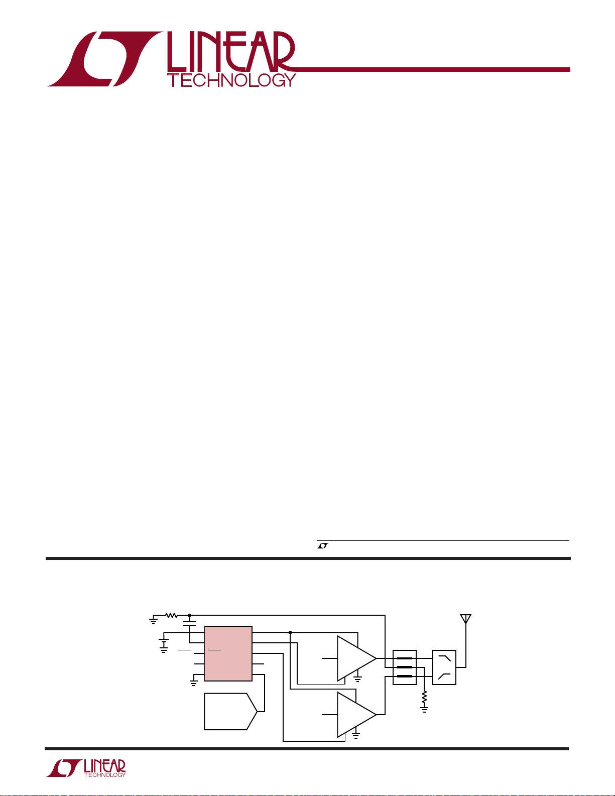
TYPICAL APPLICATIO
68Ω
33pF
V
IN
Li-Ion
SHDN
BSEL
U
LTC1758-2 Dual Band Cellular Telephone Transmitter
LTC1758-2
1
V
IN
2
RF
3
SHDN
4
BSEL
5
GND
DAC
V
V
PCA
V
PCB
TXEN
PCTL
10
CC
9
8
7
TXEN
6
900MHz
1.8GHz/1.9GHz RF PA
RF PA
DIRECTIONAL
COUPLER
DIPLEXER
50Ω
1758 TA01
1
Page 2
LTC1758-1/LTC1758-2
1
2
3
4
5
V
IN
RF
SHDN
BSEL
GND
10
9
8
7
6
V
CC
V
PCA
V
PCB
TXEN
PCTL
TOP VIEW
MS10 PACKAGE
10-LEAD PLASTIC MSOP
WWWU
ABSOLUTE AXI U RATI GS
(Note 1)
VIN to GND............................................... –0.3V to 6.5V
V
, V
PCA
Voltage ..................................... – 0.3V to 3V
PCB
PCTL Voltage ............................... –0.3V to (VIN + 0.3V)
RF Voltage ........................................ (VIN – 2.2V) to 7V
I
, Continuous....................................................... 1A
VCC
I
, 12.5% Duty Cycle.......................................... 2.5A
VCC
SHDN, TXEN, BSEL
Voltage to GND ............................ –0.3V to (VIN + 0.3V)
UU
W
PACKAGE/ORDER I FOR ATIO
TOP VIEW
V
1
IN
2
RF
3
SHDN
4
GND
MS8 PACKAGE
8-LEAD PLASTIC MSOP
T
= 125°C, θJA = 160°C/W
JMAX
Consult LTC Marketing for parts specified with wider operating temperature ranges.
8
7
6
5
V
CC
V
PCA
TXEN
PCTL
ORDER PART
NUMBER
LTC1758-1EMS8
MS8 PART MARKING
LTSL
I
, 25% Duty Cycle ...................................... 20mA
VPCA/B
Operating Temperature Range (Note 2) . –30°C to 85°C
Storage Temperature Range ................ –65°C to 150°C
Maximum Junction Temperature ........................ 125°C
Lead Temperature (Soldering, 10 sec)................ 300°C
ORDER PART
NUMBER
LTC1758-2EMS
T
= 125°C, θJA = 160°C/W
JMAX
MS10 PART MARKING
LTSM
ELECTRICAL CHARACTERISTICS
The ● denotes specifications which apply over the full operating
temperature range, otherwise specifications are at TA = 25°C. VIN = 3.6V, SHDN = TXEN = HI, unless otherwise noted.
PARAMETER CONDITIONS MIN TYP MAX UNITS
VIN Operating Voltage ● 2.7 6 V
I
Shutdown Current SHDN = LO, TXEN = LO, BSEL = LO ● 1 µA
VIN
I
Autozero Current SHDN = HI, TXEN = LO ● 1 1.6 mA
VIN
I
Operating Current SHDN = HI, TXEN = HI, I
VIN
I
Current Limit 2.2 A
VCC
VIN to VCC Resistance SHDN = LO, TXEN = LO 90 150 mΩ
V
PCA/B VOL
V
Dropout Voltage I
PCA/B
V
Voltage Clamp R
PCA/B
V
Output Current V
PCA/B
V
Enable Time V
PCA/B
V
Bandwidth C
PCA/B
V
Load Capacitance (Note 6) 100 pF
PCA/B
V
Slew Rate V
PCA/B
V
Droop VIN = 2.7V, V
PCA/B
V
TXEN Start Voltage Open Loop, TXEN Low to High, C
PCA/B
SHDN Input Threshold VIN = 2.7V to 6V, TXEN = LO ● 0.35 1.4 V
TXEN, BSEL Input Threshold VIN = 2.7V to 6V ● 0.35 1.4 V
2
TXEN = HI, Open Loop, PCTL = –100mV ● 0 0.1 V
= 5.5mA, VIN = 2.7V ● VIN – 0.28 V
LOAD
= 400Ω, PCTL = 2V, External Gain = 0.417 ● 2.7 2.85 3.0 V
LOAD
= 2.4V, VIN = 2.7V ● 5.5 9 mA
PCA/B
V
= 2.6V, VIN = 3V ● 610 mA
PCA/B
= 2V Step, C
PCTL
= 100pF, R
LOAD
= 2V Step, C
PCTL
LOAD
LOAD
LOAD
= 2V Step ±1 µV/ms
PCTL
= I
VPCA
= 100pF (Note 5) ● 620 1000 ns
= 400Ω (Note 8) ● 180 250 330 kHz
= 100pF (Note 3) ● 0.75 1.3 V/µs
= 0mA, V
VPCB
= 100pF (Note 9) 500 600 700 mV
LOAD
= HI 1.1 1.7 mA
PCA/B
Page 3
LTC1758-1/LTC1758-2
LECTRICAL C CHARA TERIST
E
ICS
The ● denotes specifications which apply over the full operating
temperature range, otherwise specifications are at TA = 25°C. VIN = 3.6V, SHDN = TXEN = VIN, unless otherwise noted.
PARAMETER CONDITIONS MIN TYP MAX UNITS
SHDN, TXEN, BSEL Input Current SHDN, TXEN or BSEL = 3.6V ● 10 25 50 µA
PCTL Input Voltage Control Range VIN = 3V to 6V, R
PCTL Input Voltage Range VIN = 3V, R
LOAD
PCTL Input Resistance SHDN = LO, TXEN = LO ● 50 90 140 kΩ
PCTL Input Filter 350 kHz
Autozero Range VIN = 2.7V, R
Autozero Settling Time (tS)t
, Shutdown to Enable (Autozero), VIN = 2.7V (Note 10) ● 50 µs
S
RF Input Frequency Range (Note 6) ● 850 2000 MHz
RF Input Power Range 900MHz (Note 6) –26 16 dBm
1800MHz (Note 6) –24 16 dBm
RF Input Impedance Referenced to VIN, SHDN = LO, TXEN = LO ● 100 200 350 Ω
BSEL Timing t1, Setup Time Prior to TXEN Asserted High 200 ns
, Hold Time After TXEN is Asserted Low 200 ns
t
2
Note 1: Absolute Maximum Ratings are those values beyond which the life
of a device may be impaired.
Note 2: The LTC1758-1 and LTC1758-2 are guaranteed to meet
performance specifications from 0°C to 70°C. Specifications over the
–30°C to 85°C operating temperature range are assured by design,
characterization and correlation with statistical process controls.
Note 3: Slew rate is measured open loop. The slew time at V
measured between 1V and 2V.
Note 4: Maximum DAC zero-scale offset voltage that can be applied to
PCTL.
= 400Ω ● 02V
LOAD
= 400Ω (Note 7) ● 2.4 V
= 400Ω (Note 4) ● 400 mV
LOAD
Note 5: This is the time from TXEN rising edge 50% switch point to
V
= 1V.
PCA/B
Note 6: Guaranteed by design. This parameter is not production tested.
Note 7: Includes maximum DAC offset voltage and maximum control
voltage.
Note 8: Bandwidth is calculated using the 10% to 90% rise time:
or V
PCB
is
BW = 0.35/rise time
PCA
Note 9: Measured 1µs after TXEN = HI.
Note 10: 50% switch point, SHDN HI = V
, TXEN HI = VIN.
IN
UW
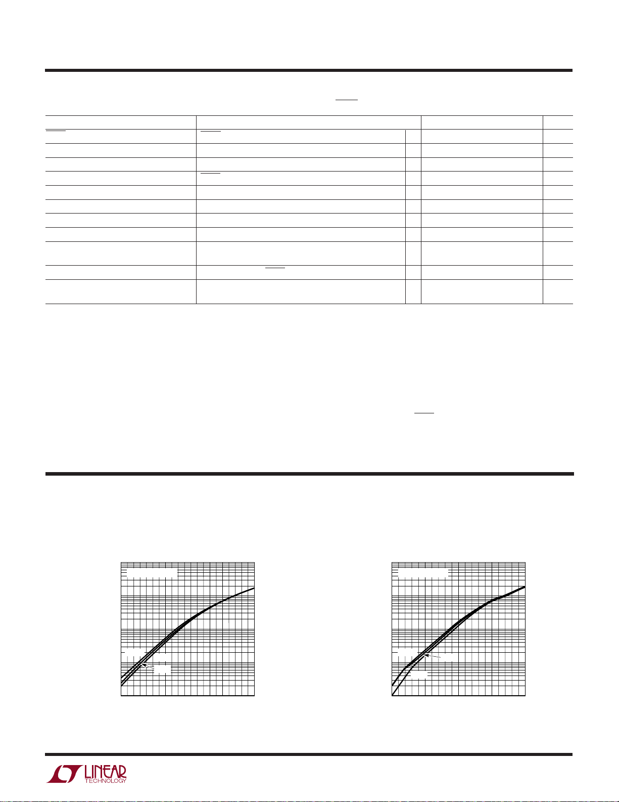
TYPICAL PERFOR A CE CHARACTERISTICS
RF Detector Characteristics
at 900MHz
10000
VIN = 3V TO 4.4V
1000
100
–30°C
10
1
–26 –14 –8 –2 4 10
PCTL REFERENCED DETECTOR OUTPUT VOLTAGE (mV)
75°C
25°C
–20
RF INPUT POWER (dBm)
16
1758 G01
RF Detector Characteristics
at 1800MHz
10000
VIN = 3V TO 4.4V
1000
100
–30°C
10
1
–24 –16 –12 –8 –4 0 4 8
PCTL REFERENCED DETECTOR OUTPUT VOLTAGE (mV)
–20
25°C
75°C
12 16
RF INPUT POWER (dBm)
1758 G02
3
Page 4

LTC1758-1/LTC1758-2
U
PI FU CTIO S
VIN (Pin 1): Input Supply Voltage, 2.7V to 6V. VIN should
be bypassed with 0.1µF and 100pF ceramic capacitors.
Used as return for RF 200Ω termination.
RF (Pin 2): RF Feedback Voltage from the Directional
Coupler. Referenced to VIN. A coupling capacitor of 33pF
must be used to connect to the ground referenced directional coupler. The frequency range is 850MHz to 2000MHz.
This pin has an internal 200Ω termination, an internal
Schottky diode detector and peak detector capacitor.
SHDN (Pin 3): Shutdown Input. A logic low on the SHDN
pin places the part in shutdown mode. A logic high places
the part in autozero when TXEN is low. SHDN has an internal 150k pull-down resistor to ensure that the part is in shutdown when the drivers are in a three-state condition.
BSEL (Pin 4): (LTC1758-2 Only) Selects V
and V
resistor to ground.
GND (Pin 5/Pin 4): System Ground.
PCTL (Pin 6/Pin 5): Analog Input. The external power
control DAC drives this input. The amplifier servos the RF
when high. This input has an internal 150k
PCB
UU
(LTC1758-2/LTC1758-1)
when low
PCA
power until the RF detected signal equals the DAC signal.
The input impedance is typically 90kΩ.
TXEN (Pin 7/Pin 6): Transmit Enable Input. A logic high
enables the control amplifier. When TXEN is low and
SHDN is high the part is in the autozero mode. This input
has an internal 150k resistor to ground.
V
(Pin 8): (LTC1758-2 Only) Power Control Voltage
PCB
Output. This pin drives an external RF power amplifier
power control pin. The maximum load capacitance is
100pF. The output is capable of rail-to-rail swings at low
load currents. Selected when BSEL is high.
V
(Pin 9/Pin 7): Power Control Voltage Output. This pin
PCA
drives an external RF power amplifier power control pin.
The maximum load capacitance is 100pF. The output is
capable of rail-to-rail swings at low load currents. Selected
when BSEL is low (LTC1758-2 only).
VCC (Pin 10/Pin 8): RF Power Amplifier Supply. This pin
has an internal 0.090Ω sense resistor between VIN and
VCC that senses the RF power amplifier supply current to
detect overcurrent conditions.
4
Page 5
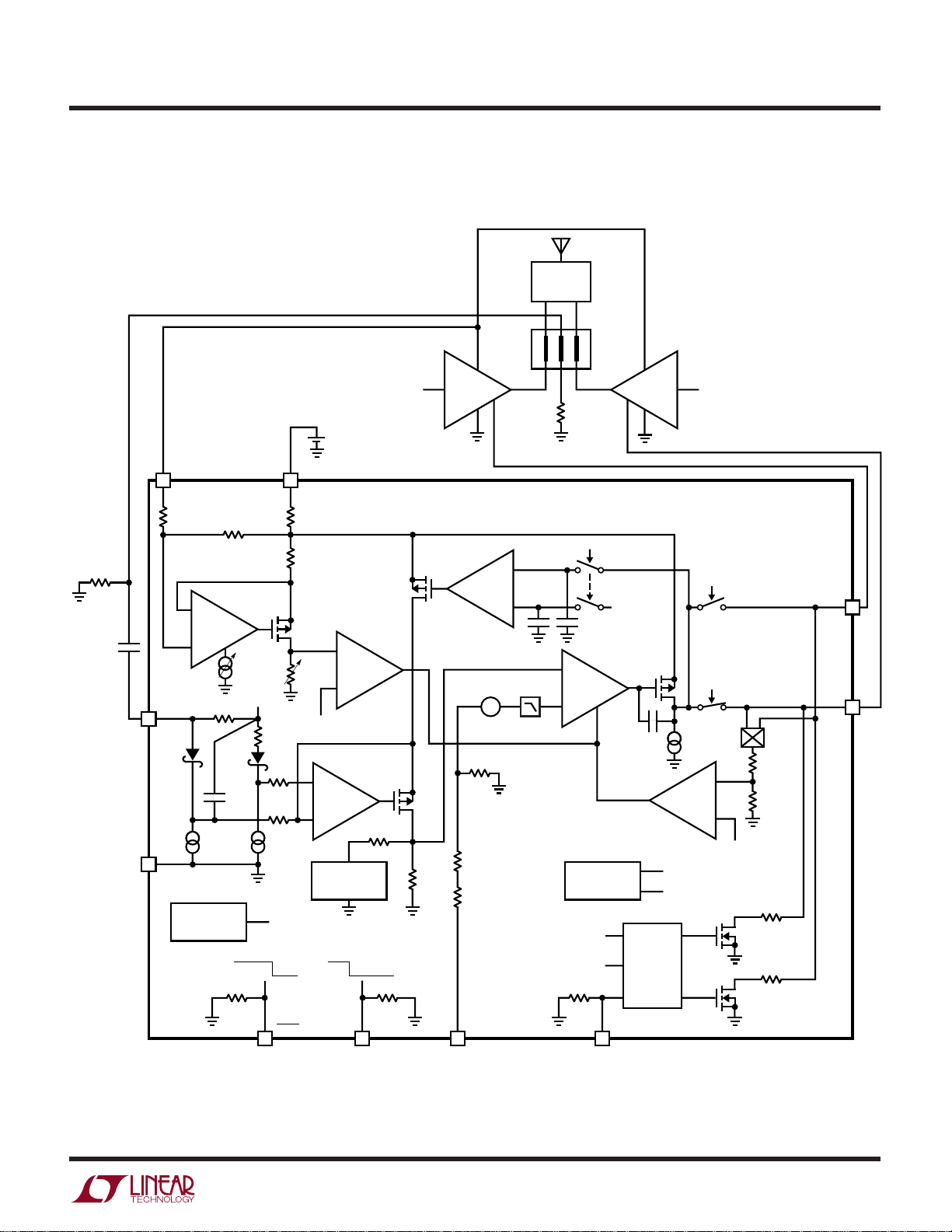
BLOCK DIAGRA
LTC1758-1/LTC1758-2
W
(LTC1758-2)
DIPLEXER
68Ω
33pF
10
V
CC
R
SENSE
0.02Ω 0.02Ω
0.05Ω
METAL
–
CS
+
OFFSET
TRIM
V
IN
RF
2
GND
5
200Ω
28pF
60µA60µA
BG1
THERMAL
SHUTDOWN
OPERATE SHDN
1
V
100Ω
METAL
OVERCURRENT
PROGRAMMABLE
200Ω
35k
35k
TSDB
Li-Ion
IN
GAIN
TRIM
+
RFDET
–
COMPRESSION
XMT AUTOZERO
RF PA900MHz
50Ω
AUTOZERO
TXENB
–
AZ
+
g
m
50mV FILTER
+
–
ICL
33k
22k
33k
22k
22k
+
CAMP
–
BG1
1.2V BANDGAP
TXENI
150k150k150k
RF PA
ADJUSTABLE
C
C
VPC
MUX
CONTROL
1.8GHz/1.9GHz
400µA
g
m
1.2V
ADJUSTABLE
PB
PA
PA
V
PCA
9
PB
140k
110k
1.2V
12Ω
100ΩTSDB
12Ω
100Ω
V
PCB
8
SHDN
TXEN
73
PCTL
6
BSEL
4
1758 BD
5
Page 6

LTC1758-1/LTC1758-2
U
WUU
APPLICATIONS INFORMATION
Forward
The LTC1758 has a wider dynamic range than the
LTC1757A. The Schottky diode detector dynamic range
has been extended to over 40dB. The start voltage accuracy has been improved to ±17%. The autozero hold time
has been increased for applications requiring transmit
times of several hundred milliseconds. The PCTL input
filter bandwidth has been reduced to 350kHz for improved
rejection of DAC noise as well as smoother ramp shaping.
The bandwidth has been reduced to 250kHz to control
slow turn-on RF power amplifiers.
Operation
The LTC1758-2 dual band RF power control amplifier
integrates several functions to provide RF power control
over frequencies ranging from 850MHz to 2GHz. The
device also prevents damage to the RF power amplifier
due to overvoltage or overcurrent conditions. These functions include an internally compensated power control,
amplifier to control the RF output power, an autozero
section to cancel internal and external voltage offsets, a
sense amplifier with an internal sense resistor to limit the
maximum RF power amplifier current, an RF Schottky
diode peak detector and amplifier to convert the RF feedback signal to DC, a V
compression, a bandgap reference, a thermal shutdown
circuit and a multiplexer to switch the control amplifier
output to either V
Band Selection
The LTC1758-2 is designed for dual band operation. The
BSEL pin will select output V
V
when high. For example, V
PCB
a 900MHz channel and V
BSEL must be established before the part is enabled. The
LTC1758-1 can be used to drive a single RF channel or
dual channel with integral multiplexer.
PCA
or V
overvoltage clamp, gain
PCA/B
.
PCB
when low and output
PCA
could be used to drive
PCA
a 1.8GHz/1.9GHz channel.
PCB
Control Amplifier
The control amplifier supplies the power control voltage to
the RF power amplifier. A portion (typically – 19dB for low
frequencies and –14dB for high frequencies) of the RF
output voltage is sampled, via a directional coupler, to
close the gain control loop. When a DAC voltage is applied
to PCTL, the amplifier quickly servos V
until the detected feedback voltage applied to the RF pin
matches the voltage at PCTL. This feedback loop provides
accurate RF power control. V
driving a 5.5mA load current and 100pF load capacitor.
RF Detector
The internal RF Schottky diode peak detector and amplifier converts the RF feedback
coupler to a low frequency
pared to the DAC
amplifier to close the RF power control loop. The RF pin
input resistance is typically 200Ω and the frequency
range of this pin is 850MHz to 2000MHz. The detector
demonstrates excel
wide range of input power. The Schottky detector is biased
at about 60µA and drives an on-chip peak detector capaci-
tor of 28pF.
Autozero
An autozero system is included to improve power programming accuracy over temperature. This section cancels internal offsets associated with the Schottky diode
detector and control amplifier. External offsets associated
with the DAC driving the PCTL pin are also cancelled.
Offset drift due to temperature is cancelled between each
burst. The maximum offset allowed at the DAC output is
limited to 400mV. Autozeroing is performed when the
part is in autozero mode (SHDN = high, TXEN = low).
When the part is enabled (TXEN = high, SHDN = high) the
autozero capacitors are held and the V
connected to the control amplifier output. The hold droop
voltage of typically < 1µV/ms provides for accurate offset
cancella
with the GSM protocol as well as with multislot protocols.
The part must be in the autozero mode for at least 50µs for
autozero to settle to the correct value.
tion over the normal 1/8 duty cycle associated
voltage
at the PCTL pin by the control
lent efficiency and linearity over a
or V
PCA
voltage
voltage
or V
PCA
are capable of
PCB
from the directional
. This
voltage
PCA
PCB
or V
positive
is com-
pin is
PCB
6
Page 7

LTC1758-1/LTC1758-2
U
WUU
APPLICATIONS INFORMATION
Filter
There is a 350kHz single pole filter included in the PCTL
path.
Protection Features
The RF power amplifier is overcurrent protected by an
internal sense amplifier. The sense amplifier measures the
voltage across an internal 0.090Ω resistor to determine
the RF power amplifier current. V
this supply current exceeds 2.2A, thereby regulating the
current to about 2.25A. The regulated current limit is
temperature compensated. The 0.090Ω resistor and the
current limit feature can be removed by connecting the PA
directly to VIN.
The RF power amplifier control voltage pins are overvoltage protected. The VPC overvoltage clamp regulates V
or V
to 2.85V when the gain and PCTL input combina-
PCB
tion attempts to exceed this voltage.
The internal thermal shutdown circuit will disable the
LTC1758-2 if the junction temperature exceeds approximately 150°C. The part will be enabled when the temperature falls below 140°C.
PCA
or V
is lowered as
PCB
PCA
Modes of Operation
The LTC1758-2 supports three operating modes: shutdown, autozero and enable.
In shutdown mode (SHDN = Low) the part is disabled and
supply currents will be reduced to <1µA. V
PCA
and V
PCB
will be connected to ground via 100Ω switches.
In autozero mode (SHDN = High, TXEN = Low) V
V
will remain connected to ground and the part will be
PCB
PCA
and
in the autozero mode. The part must remain in autozero for
at least 50µs to allow for the autozero circuit to settle.
In enable mode (SHDN = High, TXEN = High) the control
loop and protection functions will be operational. When
TXEN is switched high, acquisition will begin. The control
amplifier will start to ramp the control voltage to the RF
power amplifier. The RF amplifier will then start to turn
on. The feedback signal from the directional coupler and
the output power will be detected by the LTC1758-2 at the
RF pin. The loop closes and the amplifier output tracks
the DAC voltage ramping at PCTL. The RF power output
will then follow the programmed power profile from the
DAC.
MODE SHDN TXEN OPERATION
Shutdown Low Low Disabled
Autozero High Low Autozero
Enable High High Power Control
SHUTDOWN AUTOZERO
SHDN
BSEL
TXEN
PCTL
V
PCA
V
PCB
START
VOLTAGE
LTC1758-2 Timing Diagram
ENABLE
t
1
t
S
t
2
NOTE 1
: AUTOZERO SETTLING TIME, 50µs MINIMUM
t
S
: BSEL CHANGE PRIOR TO TXEN, 200ns TYPICAL
t
START
VOLTAGE
1
: BSEL CHANGE AFTER TXEN, 200ns TYPICAL
t
2
NOTE 1: THE EXTERNAL DAC DRIVING THE PCTL PIN CAN BE ENABLED
DURING AUTOZERO. THE AUTOZERO SYSTEM WILL CANCEL
1758 TD
THE DAC TRANSIENT. THE DAC MUST BE SETTLED TO AN OFFSET
≤400mV BEFORE TXEN IS ASSERTED HIGH.
7
Page 8

LTC1758-1/LTC1758-2
WUUU
APPLICATIO S I FOR ATIO
LTC1758-1 Description
The LTC1758-1 is identical in performance to the
LTC1758-2 except that only one control output (V
PCA
) is
available. The LTC1758-1 can drive a single band (850MHz
to 2000MHz) or a dual RF channel module with an
internal mulitplexer. Several manufacturers offer dual RF
channel modules with an internal mulitplexer.
General Layout Considerations
The LTC1758-1/LTC1758-2 should be placed near the
directional coupler. The feedback signal line to the RF pin
should be a 50Ω transmission line with optional termination or a short line. If short-circuit protection is used,
bypass capacitors are required at VCC.
External Termination
The LTC1758 has an internal 200Ω termination resistor at
the RF pin. If a directional coupler is used, it is recommended that an external 68Ω termination resistor be
connected between the RF coupling capacitor (33pF), and
ground at the side connected to the directional coupler. If
the termination is placed at the LTC1758 RF pin, then the
68Ω resistor must be connected to VIN since the detector
is referenced to VIN. Termination components should be
placed adjacent to the LTC1758.
Power Ramp Profiles
The external voltage gain associated with the RF channel
can vary significantly between RF power amplifier types.
The LTC1758 frequency compensation has been optimized to be stable with several different power amplifiers
and manufacturers. This frequency compensation generally defines the loop dynamics that impact the power/time
response and possibly (slow loops) the power ramp
sidebands. The LTC1758 operates open loop until an RF
voltage appears at the RF pin, at which time the loop closes
and the output power follows the DAC profile. The RF
power amplifier will require a certain control voltage level
(threshold) before an RF output signal is produced. The
LTC1758 V
outputs must quickly rise to this thresh-
PCA/B
old voltage in order to meet the power/time profile. To
reduce this time, the LTC1758 starts at 600mV. However,
at very low power levels the PCTL input signal is small, and
the V
outputs may take several microseconds to
PCA/B
reach the RF power amplifier threshold voltage. To reduce
this time, it may be necessary to apply a positive pulse at
the start of the ramp to quickly bring the V
PCA/B
outputs to
the threshold voltage. This can generally be achieved with
DAC programming. The magnitude of the pulse is dependent on the RF amplifier characteristics.
Power ramp sidebands and power/time are also a factor
when ramping to zero power. For RF amplifiers requiring
high control voltages, it may be necessary to further adjust
the DAC ramp profile. When the power is ramped down the
loop will eventually open at power levels below the LTC1758
detector threshold. The LTC1758 will then go open loop
and the output voltage at V
PCA
or V
will stop falling. If
PCB
this voltage is high enough to produce RF output power,
the power/time or power ramp sidebands may not meet
specification. This problem can be avoided by starting the
DAC ramp from 100mV (Figure 1). At the end of the cycle,
the DAC can be ramped down to 0mV. This applies a
negative signal to the LTC1758 thereby ensuring that the
V
outputs will ramp to 0V. The 100mV ramp step
PCA/B
must be applied at least 4µs before TXEN is asserted high
10
0
–10
–20
–30
–40
RFOUT (dBc)DAC VOLTAGE
–50
–60
–70
–80
TXEN
SHDN
–28 –18 –10 0
START
PULSE
START
CODE
100mV
50µs MINIMUM, ALLOWS TIME FOR DAC
AND AUTOZERO TO SETTLE
Figure 1. LTC1758 Ramp Timing
TIME (µs)
543 553 561 571
ZERO
CODE
1758 F01
8
Page 9

WUUU
APPLICATIO S I FOR ATIO
LTC1758-1/LTC1758-2
to allow the autozero to cancel the step. Slow DAC rise
times will extend this time by the additional RC time
constants.
Another factor that affects power ramp sidebands is the
DAC signal to PCTL. The bandwidth of the LTC1758 may
not be low enough to adequately filter out steps associated
with the DAC. If the baseband chip does not have an
internal filter, it is recommended that a 1-stage external
filter be placed between the DAC output and the PCTL pin.
Resistor values should be kept below 2k since the PCTL
input resistance is 90k. A typical filter scheme is shown in
Figure 2.
The power control ramp should be started in the range of
1µs to 10µs after TXEN is asserted high.
DAC
2k
Figure 2
LTC1758
PTCL
330pF
1758 F02
Demo Board
The LTC1758 demo board is available upon request. The
demo board has a 900MHz and an 1800MHz RF channel
controlled by the LTC1758. Timing signals for TXEN are
generated on the board using a 13MHz crystal reference.
The PCTL power control pin is driven by a 10-bit DAC and
the DAC profile can be loaded via a serial port. The serial
port data is stored in a flash memory which is capable of
storing eight ramp profiles. The board is supplied preloaded
with four GSM power profiles and four DCS power profiles
covering the entire power range. External timing signals
can be used in place of the internal crystal controlled
timing. A variety of RF power amplifiers are available.
LTC1758 Control Loop Stability
The LTC1758 provides a stable control loop for several RF
power amplifier models from different manufacturers
over a wide range of frequencies, output power levels and
V
conditions. However, there are several factors that
SWR
can improve or degrade loop frequency stability.
1) The additional voltage gain supplied by the RF power
amplifier increases the loop gain raising poles normally
below the 0dB axis. The extra voltage gain can vary
significantly over input/output power ranges, frequency,
power supply, temperature and manufacturer. RF power
amplifier gain control transfer functions are often not
available and must be generated by the user. Loop oscillations are most likely to occur in the midpower range
where the external voltage gain associated with the RF
power amplifier typically peaks. It is useful to measure the
oscillation or ringing frequency to determine whether it
corresponds to the expected loop bandwidth and thus is
due to high gain bandwidth.
2) Loop voltage losses supplied by the directional coupler
will improve phase margin. The larger the directional
coupler loss the more stable the loop will become. However, larger losses reduce the RF signal to the LTC1758
and detector performance may be degraded at low power
levels. (See RF Detector Characteristics.)
3) Additional poles within the loop due to filtering or the
turn-on response of the RF power amplifier can degrade
the phase margin if these pole frequencies are near the
effective loop bandwidth frequency. Generally loops using
RF power amplifiers with fast turn-on times have more
phase margin. Extra filtering below 16MHz should never
be placed within the control loop, as this will only degrade
phase margin.
4) Control loop instability can also be due to open loop
issues. RF power amplifiers should first be characterized
in an open loop configuration to ensure self oscillation is
not present. Self-oscillation is often related to poor power
supply decoupling, ground loops, coupling due to poor
layout and extreme V
conditions. The oscillation fre-
SWR
quency is generally in the 100kHz to 10MHz range. Power
supply related oscillation suppression requires large value
ceramic decoupling capacitors placed close to the RF
power amp supply pins. The range of decoupling capacitor
values is typically 1nF to 3.3µF.
5) Poor layout techniques associated with the directional
coupler area may result in high frequency signals bypassing the coupler. This could result in stability problems due
to the reduction in the coupler loss.
9
Page 10

LTC1758-1/LTC1758-2
WUUU
APPLICATIO S I FOR ATIO
Determining External Loop Gain and Bandwidth
The external loop voltage gain contributed by the RF channel and directional coupler network should be measured in
a closed loop configuration. A voltage step is applied to
PCTL and the change in V
PCA
(or V
) is measured. The
PCB
detected voltage is 0.6 • PCTL for PCTL < 640mV and
1.18PCTL – 0.38V for PCTL > 640mV. The external voltage
gain contributed by the RF power amplifier and directional
coupler network is 0.6 • ∆V
0.38V) • ∆V
PCTL
/∆V
. Measuring voltage gain in the
PCA
PCTL
/∆V
and (1.18PCTL –
VPCA
closed loop configuration accounts for the nonlinear detector gain that is dependent on RF input voltage and
frequency.
The LTC1758 unity gain bandwidth specified in the data
sheet assumes that the net voltage gain contributed by the
RF power amplifier and directional coupler is unity. The
bandwidth is calculated by measuring the rise time between 10% and 90% of the voltage change at V
PCA
or V
PCB
for a small step in voltage applied to PCTL.
BW1 = 0.35/rise time
The LTC1758 control amplifier unity gain bandwidth (BW1)
is typically 250kHz. The phase margin of the control
amplifier is typically 90°.
For example, to determine the external RF channel loop
voltage gain with the loop closed, apply a 100mV step to
PCTL from 300mV to 400mV. V
PCA
(or V
) will increase
PCB
to supply enough feedback voltage to the RF pin to cancel
this 100mV step which would be the required detected
voltage of 60mV. V
changed from 1.498V to 1.540V to
PCA
create the RF output power change required. The net
external voltage gain contributed by the RF power amplifier and directional coupler network can be calculated by
dividing the 60mV change at the RF pin by the 42mV
change at the V
pin. The net external voltage gain would
PCA
then be approximately 1.4. The loop bandwidth extends to
1.4␣ • BW1. If BW1 is 250kHz, the loop bandwidth increases to approximately 350kHz. The phase margin is
extracted from Figure 3. Repeat the above voltage gain
measurement over the full power and frequency range.
The phase margin degradation, due to external and internal pole combinations, is difficult to determine since
complex poles are present. Gain peaking may occur,
resulting in higher bandwidth and lower phase margin
than predicted from the open loop Bode plot. A low
frequency AC SPICE model of the LTC1758 power controller is included to better determine pole and zero interactions. The user can apply external gains and poles to
determine bandwidth and phase margin. DC, transient and
RF information cannot be extracted from the present
model. The model is suitable for external gain evaluations
up to 6×. The 350kHz PCTL input filter limits the bandwidth, therefore, use the RF input as demonstrated in the
model.
80
70
60
50
40
30
20
10
0
–10
VOLTAGE GAIN (dB)
–20
–30
–40
–50
–60
1k 10k 100k 1M 10M
100
PHASE
GAIN
FREQUENCY (Hz)
R
C
LOAD
LOAD
= 2k
= 33pF
1758 F03
140
130
120
110
100
90
80
70
60
50
40
30
20
10
0
PHASE (DEG)
Figure 3. Measured Open Loop Gain and Phase, PCTL < 640mV
10
80
70
60
50
40
30
20
10
0
–10
VOLTAGE GAIN (dB)
–20
–30
–40
–50
–60
1k 10k 100k 1M 10M
100
PHASE
GAIN
FREQUENCY (Hz)
R
C
LOAD
LOAD
= 2k
= 33pF
1758 F04
150
140
130
120
110
100
90
80
70
60
50
40
30
20
10
PHASE (DEG)
Figure 4. Measured Open Loop Gain and Phase, PCTL > 640mV
Page 11

WUUU
APPLICATIO S I FOR ATIO
LTC1758-1/LTC1758-2
This model (Figure 7) is being supplied to LTC users as an
aid to circuit designs. While the model reflects close
similarity to corresponding devices in low frequency AC
performance terms, its use is not suggested as a replacement for breadboarding. Simulation should be used as a
forerunner or a supplement to traditional lab testing.
Users should note very carefully the following factors
regarding this model: Model performance in general will
reflect typical baseline specs for a given device, and
certain aspects of performance may not be modeled fully.
While reasonable care has been taken in the preparation,
we cannot be responsible for correct application on any
and all computer systems. Model users are hereby notified
that these models are supplied “as is”, with no direct or
implied responsibility on the part of LTC for their operation
within a customer circuit or system. Further, Linear Technology Corporation reserves the right to change these
models without prior notice.
In all cases, the current data sheet information is your final
design guideline, and is the only performance guarantee.
For further technical information, refer to individual device
data sheets. Your feedback and suggestions on this model
is appreciated.
Linear Technology Corporation hereby grants the users of
this model a nonexclusive, nontransferable license to use
this model under the following conditions:
The user agrees that this model is licensed from Linear
Technology and agrees that the model may be used,
loaned, given away or included in other model libraries as
long as this notice and the model in its entirety and
unchanged is included. No right to make derivative works
or modifications to the model is granted hereby. All such
rights are reserved.
This model is provided as is. Linear Technology makes no
warranty, either expressed or implied about the suitability
or fitness of this model for any particular purpose. In no
event will Linear Technology be liable for special, collateral, incidental or consequential damages in connection
with or arising out of the use of this model. It should be
remembered that models are a simplification of the actual
circuit.
CONTROL
AMPLIFER
BW1 ≅ 250kHz RF POWER AMP
+
I
FB
G1PCTL
–
LTC1758
H1
RF DETECTOR
V
PCA/B
RF
DIRECTIONAL
COUPLER
14dB to 20dB LOSS
G2
H2
CONTROLLED
RF OUTPUT
POWER
1758 F05
Figure 5. Closed Loop Block Diagram
80
70
60
50
40
30
20
10
0
–10
VOLTAGE GAIN (dB)
–20
–30
–40
–50
–60
1k 10k 100k 1M 10M
100
PHASE
GAIN
FREQUENCY (Hz)
R
C
LOAD
LOAD
= 2k
= 33pF
1758 F06
120
110
100
90
80
70
60
50
40
30
20
10
0
–10
–20
PHASE (DEG)
Figure 6. SPICE Model Open Loop Gain and Phase
Characteristics from RF to V
, PCTL < 640mV
PCA
11
Page 12

LTC1758-1/LTC1758-2
WUUU
APPLICATIO S I FOR ATIO
*LTC1758 Low Frequency AC Spice Model*
GIN1 ND2 0 ND1A IFB 100E-6
GX3 ND6 0 0 ND4 1E-6
GX4 ND7 0 0 ND6 1E-6
GX1 ND3 0 0 ND2 1E-6
GX2 ND4 0 0 ND3 1E-6
GX5 ND10 0 0 ND9 1E-6
GX8 ND14 0 0 ND12 1E-6
GX7 ND12 0 0 ND11 1E-6
GX6 ND11 0 0 ND10 1E-6
GXFB IFB 0 0 ND14 28.8E-6
EX1 ND8 0 0 ND7 1
RPCTL2 ND1 0 33E3
RFILT ND1 ND1A 50E3
RO1 ND2 0 70E6
RX3 ND6 0 1E6
RX4 ND7 0 1E6
RPCTL1 PCTL ND1 53E3
RX1 ND3 0 1E6
RX2 ND4 ND5 1E6
RSD RF ND9 500
RX5 ND10 0 1E6
RT RF 0 250
RX8 ND14 0 1E6
RX7 ND12 ND13 1E6
RX6 ND11 0 1E6
R9 ND8 ND8A 100
R9A ND8A VPCA 20
RLOAD VPCA 0 2E3
RFB1 IFB 0 22E3
CPCTL1 ND1A 0 7E-12
CX3 ND6 0 8E-15
CX4 ND7 0 12E-15
CC1 ND2 0 45E-12
CX1 ND3 0 2E-15
CX5 ND10 0 10E-15
CX6 ND11 0 1.2E-15
CLOAD VPCA 0 33E-12
CLINT ND8A 0 37E-12
CLINTA VPCA 0 18E-12
CFB1 IFB 0 300E-15
CP ND9 0 28E-12
LX2 ND5 0 34E-3
LX7 ND13 0 7E-3
**Closed loop connections, comment-out VPCTLO, VRF, Adjust EFB gain to reflect external gain, currently set at 3X**
*EFB RF 0 VPCA VIN 3
VIN VIN 0 DC 0 AC 1
*VPCTLO PCTL 0 DC 0
**Open loop connections, comment-out EFB, VIN and VPCTLO**
VPCTLO PCTL 0 DC 0
VRF RF 0 DC 0 AC 1
**Add AC statement and print statement as required**
.AC DEC 50 100 1E7
.END
Figure 7. LTC1758 Low Frequency AC SPICE Model
12
Page 13

WUUU
APPLICATIO S I FOR ATIO
ND7
X4
C
RX41E6
12E-15
V
PCA
LOAD
C
LTC1758-1/LTC1758-2
33E-12
13MHz POLE
GX4
ND6
20MHz POLE
GX3
ND4
RX21E6
5MHz ZERO
GX2
ND3
80MHz POLE
GX1
+
RX31E6
+
+
RX11E6
+
GM
GM
ND5
2E3
LOAD
R9A
R9
EX1
+
+
20Ω
ND8A
100Ω
ND8
VAMP
FB1
C
300E-15
FB1
R
22E3
GM
R
–
–
LINTA
C
LINT
C
18E-12
37E-12
28.8E-6
ND14
GX8
+
ND12
RX71E6
23MHz ZERO
GX7
+
ND11
130MHz POLE
GX6
+
ND10
RX81E6
GM
ND13
GM
RX61E6
GM
RX51E6
–
–
–
1E-6
X7
L
1E-6
C
1E-6
7E-3
X6
X5
C
1758 F08
1.2E-15
Figure 8. LTC1758 Low Frequency AC Model
10E-15
1E-6
–
X3
C
8E-15
1E-6
–
X2
34E-3
L
1E-6
–
X1
C
2E-15
GXFB
24MHz POLE
1E-6
–
ND2
50Hz POLE
53E3
PCTL1
R
PCTL
GIN1
ND1AND1
C1
C
RO1
70E6
45E-12
100E-6
FB
–
PCTL1
C
I
7E-12
GM GM GM
+
FILT
50E3
R
33E3
PCTL2
R
16MHz POLE
GX5
RT200Ω
RF
1E-6
GM
+
–
ND9
SD
P
R
C
500Ω
28E-12
13
Page 14

LTC1758-1/LTC1758-2
PACKAGE DESCRIPTIO
U
MS8 Package
8-Lead Plastic MSOP
(Reference LTC DWG # 05-08-1660)
0.118 ± 0.004*
(3.00 ± 0.102)
8
7
6
5
0.193 ± 0.006
(4.90 ± 0.15)
12
0.043
(1.10)
MAX
0.007
(0.18)
0.021
± 0.006
(0.53 ± 0.015)
* DIMENSION DOES NOT INCLUDE MOLD FLASH, PROTRUSIONS OR GATE BURRS. MOLD FLASH,
PROTRUSIONS OR GATE BURRS SHALL NOT EXCEED 0.006" (0.152mm) PER SIDE
** DIMENSION DOES NOT INCLUDE INTERLEAD FLASH OR PROTRUSIONS.
INTERLEAD FLASH OR PROTRUSIONS SHALL NOT EXCEED 0.006" (0.152mm) PER SIDE
° – 6° TYP
0
SEATING
PLANE
0.009 – 0.015
(0.22 – 0.38)
0.0256
(0.65)
BSC
4
3
0.118 ± 0.004**
(3.00 ± 0.102)
0.034
(0.86)
REF
0.005
± 0.002
(0.13 ± 0.05)
MSOP (MS8) 1100
14
Page 15

PACKAGE DESCRIPTIO
U
MS10 Package
10-Lead Plastic MSOP
(Reference LTC DWG # 05-08-1661)
0.118 ± 0.004*
(3.00 ± 0.102)
LTC1758-1/LTC1758-2
8910
7
6
0.193 ± 0.006
(4.90 ± 0.15)
45
12
3
0.043
(1.10)
(0.17 – 0.27)
MAX
0.0197
(0.50)
BSC
0.007
(0.18)
0.021
± 0.006
(0.53 ± 0.015)
* DIMENSION DOES NOT INCLUDE MOLD FLASH, PROTRUSIONS OR GATE BURRS. MOLD FLASH,
PROTRUSIONS OR GATE BURRS SHALL NOT EXCEED 0.006" (0.152mm) PER SIDE
** DIMENSION DOES NOT INCLUDE INTERLEAD FLASH OR PROTRUSIONS.
INTERLEAD FLASH OR PROTRUSIONS SHALL NOT EXCEED 0.006" (0.152mm) PER SIDE
° – 6° TYP
0
SEATING
PLANE
0.007 – 0.011
0.118 ± 0.004**
(3.00 ± 0.102)
0.034
(0.86)
REF
0.005
± 0.002
(0.13 ± 0.05)
MSOP (MS10) 1100
Information furnished by Linear Technology Corporation is believed to be accurate and reliable.
However, no responsibility is assumed for its use. Linear Technology Corporation makes no representation that the interconnection of its circuits as described herein will not infringe on existing patent rights.
15
Page 16

LTC1758-1/LTC1758-2
U
TYPICAL APPLICATIO S
68Ω
33pF
V
Li-Ion
IN
Li-Ion
68Ω
33pF
V
IN
SHDN
1
2
3
4
1
V
IN
2
RF
3
SHDN
SHDN
4
GND
Dual Band Cellular Telephone Transmitter Without Current Limiting
LTC1758-1 RF POWER MODULE WITH MUX
V
IN
RF
SHDN
GND
V
TXEN
PCTL
Single Band Cellular Telephone Transmitter
LTC1758-1
DAC
8
V
CC
7
PCA
6
5
V
V
PCA
TXEN
PCTL
TXEN
8
CC
7
6
TXEN
5
RF IN
V
CC
PWRCTRL
BANDSELECT
RF1 IN RF2 IN
RF PA
RFOUT1
900MHz
RFOUT2
1800MHz
DIRECTIONAL
COUPLER
1758 TA02
DIRECTIONAL
COUPLER DIPLEXER
50Ω
1758 TA03
DAC
900MHz 1800MHz
RELATED PARTS
PART NUMBER DESCRIPTION COMMENTS
LTC1261 Regulated Inductorless Voltage Inverter Regulated –5V from 3V, REG Pin Indicates Regulation, Up to 15mA, Micropower
LTC1550/LTC1551 Low Noise Inductorless Voltage Inverter Regulated Output, <1mV
LTC1730 Li-Ion Pulse Charger Complete Pulse Charger for 1-Cell Li-Ion Battery
LTC1732 Li-Ion Linear Charger Complete Linear Charger for 1- and 2-Cell Li-Ion Battery
LTC1734 ThinSOTTM Li-Ion Linear Charger Only Two External Components, Allows Charge Current Monitoring for Termination
LTC1754 ThinSOT Charge Pump 2V ≤ VIN ≤ 4V, I
LT®1761 ThinSOT LDO I
= 100mA, Low Noise: 20µV
OUT
OUT
LTC1957 RF Power Controller Single/Dual Channel RF Power Controller (Higher Bandwidth Version of the LTC1758)
LTC3200/LTC3200-5 Low Noise, Regulated Charge Pump 2MHz Constant Frequency, I
ThinSOT and MSOP Packages
LTC3404 Step-Down DC/DC Converter 1.4MHz Integrated Synchronous Rectification, 10µA Quiescent Current
ThinSOT is a trademark of Linear Technology Corporation.
Linear Technology Corporation
16
1630 McCarthy Blvd., Milpitas, CA 95035-7417
(408) 432-1900 ● FAX: (408) 434-0507
●
www.linear-tech.com
Ripple, 900kHz
P-P
= 40mA, No Inductors for White LED Backlight
RMS
= 100mA, 2.7V ≤ VIN ≤ 4.5V,
OUT
175812f LT/TP 0601 2K • PRINTED IN THE USA
LINEAR TECHNOLOGY CORPORATION 2001
 Loading...