

Page 1
FEATURES
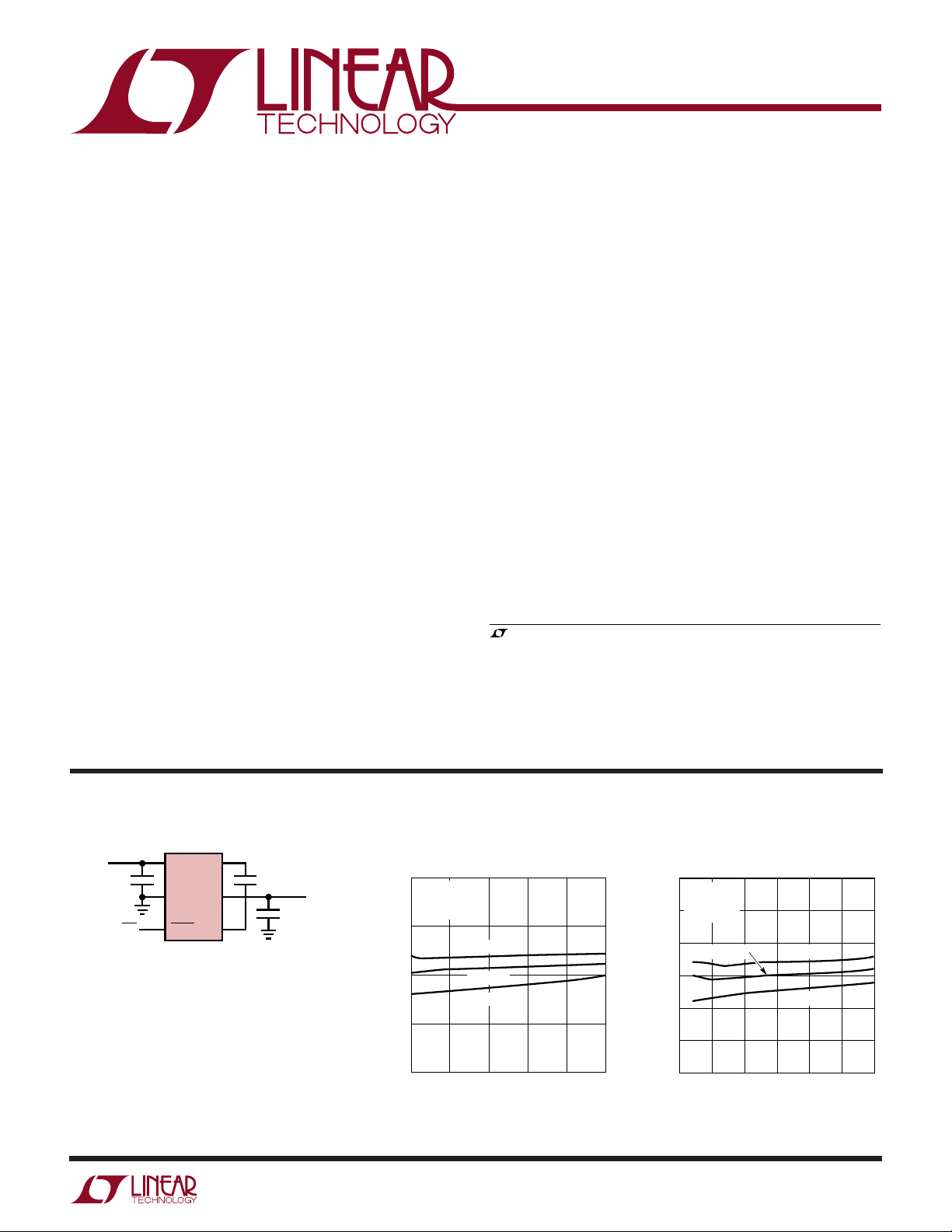
SUPPLY VOLTAGE (V)
2.5
4.85
OUTPUT VOLTAGE (V)
4.90
4.95
5.00
5.05
5.15
3.0
3.5 4.0 4.5
1574 TA03
5.0 5.5
5.10
TA = –40°C
T
A
= 85°C
I
OUT
= 25mA
C
OUT
= 10µF
C
FLY
= 1µF
TA = 25°C
■
Ultralow Power: IIN = 13µA
■
Regulated Output Voltage: 3.3V ±4%, 5V ±4%
■
5V Output Current: 50mA (VIN ≥ 3.0V)
■
3.3V Output Current: 40mA (VIN ≥ 2.5V)
■
No Inductors Needed
■
Very Low Shutdown Current: <1µA
■
Shutdown Disconnects Load from V
■
Internal Oscillator: 600kHz
■
Short-Circuit and Overtemperature Protected
■
Ultrasmall Application Circuit: (0.052 Inch2)
■
6-Pin SOT-23 Package
IN
U
APPLICATIO S
LTC1754-3.3/LTC1754-5
Micropower, Regulated
3.3V/5V Charge Pump with
Shutdown in SOT-23
U
DESCRIPTIO
The LTC®1754 is a micropower charge pump DC/DC
converter that produces a regulated output. The input
voltage range is 2V to 4.4V for 3.3V output and 2.7V to
5.5V for 5V output. Extremely low operating current and a
low external parts count (one flying capacitor and two
small bypass capacitors at VIN and V
ideally suited for small, battery-powered applications. The
total component area of the application circuit shown
below is only 0.052 inch2.
The LTC1754 operates as a Burst ModeTM switched capacitor voltage doubler to produce a regulated output. It has
thermal shutdown capability and can survive a continuous
short circuit from V
to GND.
OUT
) make the LTC1754
OUT
■
SIM Interface Supplies for GSM Cellular Telephones
■
White LED Power Supplies
■
Li-Ion Battery Backup Supplies
■
Handheld Computers
■
Smart Card Readers
■
PCMCIA Local 5V Supplies
TYPICAL APPLICATIO
V
OUT
Regulated 3.3V Output from 2V to 4.4V Input
Regulated 5V Output from 2.7V to 5.5V Input
10µF
ON/OFF
1
2
3
= 0mA TO 20mA, VIN > 2.0V
I
OUT
= 0mA TO 40mA, VIN > 2.5V
I
OUT
= 0mA TO 25mA, VIN > 2.7V
I
OUT
= 0mA TO 50mA, VIN > 3.0V
I
OUT
V
OUT
LTC1754-X
GND
SHDN
V
= 3.3V ±4%
OUT
V
= 5V ±4%
OUT
+
C
V
IN
–
C
The LTC1754 is available in a 6-pin SOT-23 package.
, LTC and LT are registered trademarks of Linear Technology Corporation.
Burst Mode is a trademark of Linear Technology Corporation.
U
LTC1754-3.3
6
1µF
5
4
10µF
1754 TA01
V
IN
Output Voltage vs Supply Voltage
3.40
I
= 20mA
OUT
C
= 10µf
OUT
= 1µF
C
FLY
3.35
= 85°C
T
A
3.30
OUTPUT VOLTAGE (V)
3.25
3.20
2.0
T
= 25°C
A
TA = –40°C
2.5
3.0
SUPPLY VOLTAGE (V)
3.5
4.0
4.5
1754 TA02
Output Voltage vs Supply Voltage
LTC1754-5
1
Page 2
LTC1754-3.3/LTC1754-5
WWWU
ABSOLUTE AXI U RATI GS
PACKAGE/ORDER I FOR ATIO
UU
W
(Note 1)
VIN to GND .................................................. – 0.3V to 6V
V
to GND ............................................... – 0.3V to 6V
OUT
SHDN to GND.............................................. – 0.3V to 6V
I
(Note 4) ......................................................... 75mA
OUT
V
Short-Circuit Duration ............................ Indefinite
OUT
Operating Temperature Range (Note 3) ... – 40°C to 85°C
Storage Temperature Range .................. –65°C to 150°C
V
OUT
GND 2
SHDN 3
TOP VIEW
1
S6 PACKAGE
6-LEAD PLASTIC SOT-23
T
= 150°C, θJA = 230°C/ W
JMAX
6 C
5 V
4 C
+
IN
–
Lead Temperature (Soldering, 10 sec)................... 300°C
Consult factory for Industrial and Military grade parts.
ELECTRICAL CHARACTERISTICS
temperature range, otherwise specifications are at TA = 25°C. C
SYMBOL PARAMETER CONDITIONS MIN TYP MAX UNITS
LTC1754-3.3
V
IN
V
OUT
I
CC
V
R
η Efficiency VIN = 2.0V, I
f
OSC
t
ON
I
SC
LTC1754-5
V
IN
V
OUT
I
CC
V
R
η Efficiency VIN = 3V, I
f
OSC
t
ON
I
SC
LTC1754-3.3/LTC1754-5
I
SHDN
V
IH
V
IL
I
IH
I
IL
Note 1: Absolute Maximum Ratings are those values beyond which the life of
a device may be impaired.
Note 2: 0.6µF is the minimum required C
current capability. Depending on the choice of capacitor material, a
somewhat higher value of capacitor may be required to attain 0.6µF over
temperature.
Input Supply Voltage ● 2.0 4.4 V
Output Voltage 2.0V ≤ VIN ≤ 4.4V, I
Operating Supply Current 2.0V ≤ VIN ≤ 4.4V, I
Output Ripple VIN = 2.5V, I
Switching Frequency Oscillator Free Running 600 kHz
V
Turn-On Time VIN = 2.0V, I
OUT
Output Short-Circuit Current VIN = 2.5V, V
Input Supply Voltage ● 2.7 5.5 V
Output Voltage 2.7V ≤ VIN ≤ 5.5V, I
Operating Supply Current 2.7V ≤ VIN ≤ 5.5V, I
Output Ripple VIN = 3V, I
Switching Frequency Oscillator Free Running 700 kHz
V
Turn-On Time VIN = 3V, I
OUT
Output Short-Circuit Current VIN = 3V, V
Shutdown Supply Current VIN ≤ 3.6V, I
SHDN Input Threshold (High) ● 1.4 V
SHDN Input Threshold (Low) ● 0.3 V
SHDN Input Current (High) SHDN = V
SHDN Input Current (Low) SHDN = 0V ● –1 1 µA
capacitance for rated output
FLY
2.5V ≤ V
3.0V ≤ VIN ≤ 5.5V, I
3.6V < V
The ● denotes specifications which apply over the full operating
= 1µF (Note 2), CIN = 10µF, C
FLY
≤ 20mA ● 3.17 3.30 3.43 V
≤ 4.4V, I
IN
OUT
OUT
OUT
, I
IN
IN
OUT
≤ 40mA ● 3.17 3.30 3.43 V
OUT
= 0mA, SHDN = V
OUT
= 40mA 23 mV
OUT
= 20mA 82 %
OUT
= 0mA 0.8 ms
OUT
= 0V, SHDN = 2.5V 118 mA
OUT
≤ 25mA ● 4.8 5.0 5.2 V
OUT
≤ 50mA ● 4.8 5.0 5.2 V
OUT
= 0mA, SHDN = V
OUT
= 50mA 65 mV
= 50mA 82.7 %
= 0mA 0.4 ms
= 0V, SHDN = 3V 150 mA
OUT
= 0mA, V
OUT
= 0mA, V
OUT
Note 3: The LTC1754ES6-X is guaranteed to meet performance
specifications from 0°C to 70°C. Specifications over the –40°C to 85°C
operating temperature range are assured by design, characterization and
correlation with statistical process controls.
Note 4: Based on long term current density limitations.
= 0V ● 0.01 1 µA
SHDN
= 0V ● 2.5 µA
SHDN
IN
IN
= 10µF.
OUT
● 11 30 µA
● 13 30 µA
● –1 1 µA
ORDER PART
NUMBER
LTC1754ES6-3.3
LTC1754ES6-5
S6 PART MARKING
LTGK
LTLW
P-P
P-P
2
Page 3
UW
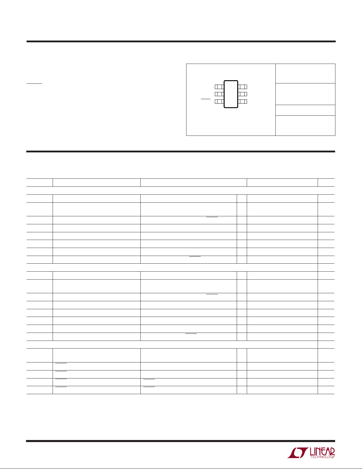
TYPICAL PERFOR A CE CHARACTERISTICS
No Load Supply Current
vs Supply VoltageOutput Voltage vs Output Current Supply Current vs V
3.40
TA = 25°C
= 10µF
C
OUT
= 1µF
C
FLY
3.35
3.30
OUTPUT VOLTAGE (V)
3.25
VIN = 2.5V
VIN = 2V
20
I
= 0µA
OUT
= 1µF
C
FLY
= V
V
SHDN
IN
15
10
SUPPLY CURRENT (µA)
TA = 85°C
TA = 25°C
TA = –40°C
LTC1754-3.3/LTC1754-5
LTC1754-3.3, TA = 25°C unless otherwise noted.
SHDN
20
TA = 25°C
= 0µA
I
OUT
15
VIN = 2.5V
10
V
= 2V
IN
SUPPLY CURRENT (µA)
5
V
= 4.5V
IN
3.20
0
I
OUT
0mA to 20mA
10mA/DIV
V
OUT
AC COUPLED
20mV/DIV
20
OUTPUT CURRENT (mA)
60
40
V
OUT
80
Short-Circuit Current
vs Supply Voltage
180
TA = 25°C
= 1µF
C
FLY
160
140
120
100
SHORT-CIRCUIT CURRENT (mA)
80
OUT
V
60
2.0
2.5 3.0 3.5 4.0
SUPPLY VOLTAGE (V)
Load Transient Response
1754 G01
100
5
2.0
1735 G04
V
OUT
AC COUPLED
20mV/DIV
2.5 3.0 3.5 4.0
SUPPLY VOLTAGE (V)
EFFICIENCY (%)
4.5
Output Ripple
4.5
1754 G02
0
Efficiency vs Load Current
100
TA = 25°C
90
V
= 2V
IN
= 1µF
C
FLY
80
70
60
50
40
30
20
10
0
0.01 0.1 1 10 100
0.001
LOAD CURRENT (mA)
SHDN
1V/DIV
V
OUT
1V/DIV
1
2
V
CONTROL VOLTAGE (V)
SHDN
1754 G05
Start-Up Time
3
4
5
1754 G03
= 2V 50µs/DIV 1754 G07
V
IN
C
= 10µF
OUT
= 2V 5µs/DIV 1754 G08
V
IN
C
= 10µF
OUT
= 20mA
I
OUT
= 2V 200µs/DIV 1754 G9
V
IN
C
= 10µF
OUT
3
Page 4
LTC1754-3.3/LTC1754-5
UW
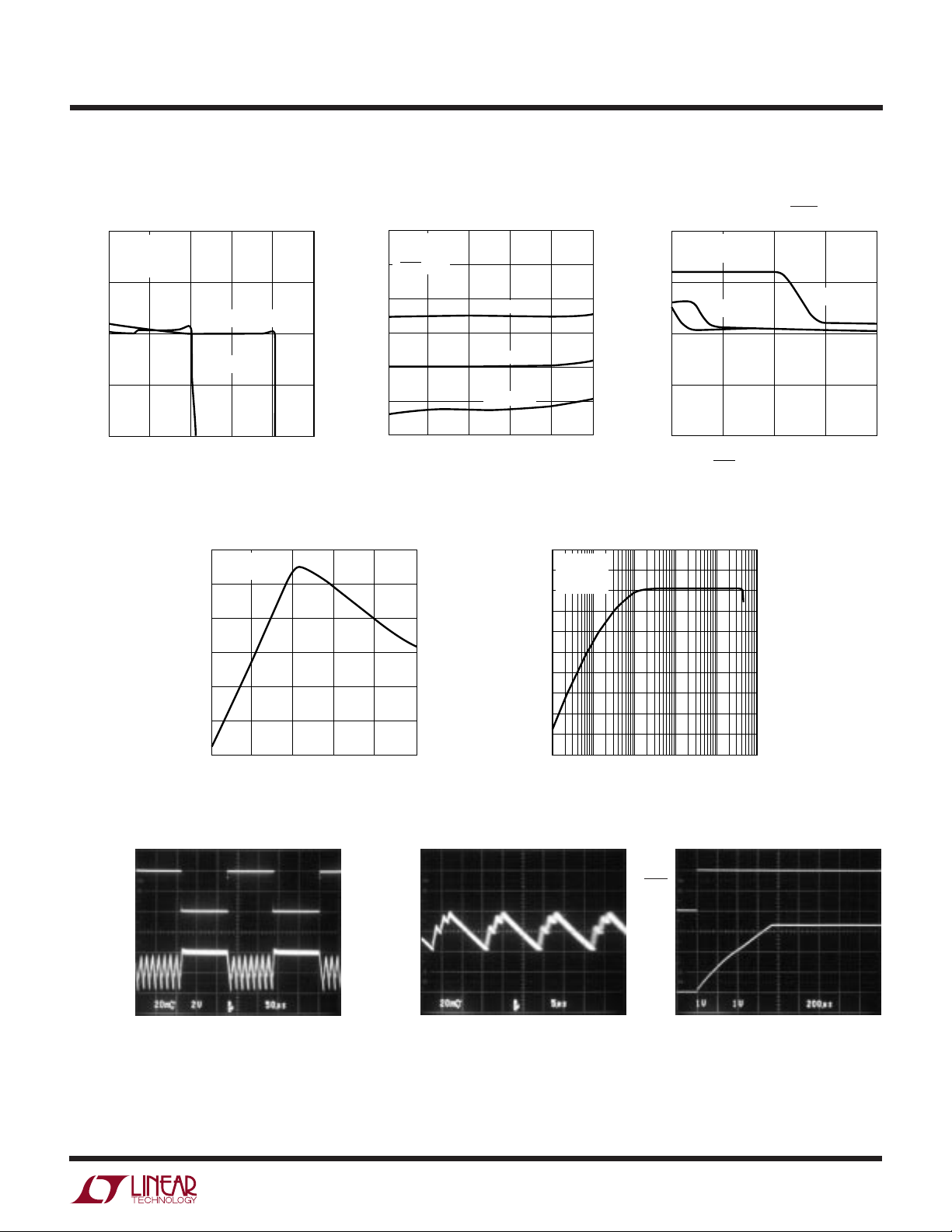
TYPICAL PERFOR A CE CHARACTERISTICS
No Load Supply Current
vs Supply VoltageOutput Voltage vs Output Current Supply Current vs V
5.15
TA = 25°C
= 10µF
C
OUT
5.10
5.05
5.00
4.95
OUTPUT VOLTAGE (V)
4.90
= 1µF
C
FLY
VIN = 3V
VIN = 2.7V
20
I
= 0µA
OUT
C
= 1µF
FLY
V
= V
SHDN
IN
15
10
SUPPLY CURRENT (µA)
TA = 85°C
TA = 25°C
TA = –40°C
LTC1754-5, TA = 25°C unless otherwise noted.
SHDN
25
TA = 25°C
I
= 0µA
OUT
20
VIN = 3.3V
15
VIN = 2.7V
10
SUPPLY CURRENT (µA)
5
V
= 5.5V
IN
4.85
0
I
OUT
0mA to 50mA
25mA/DIV
V
OUT
AC COUPLED
50mV/DIV
20 40 60 80
OUTPUT CURRENT (mA)
V
Short-Circuit Current
OUT
vs Supply Voltage
220
TA = 25°C
C
= 1µF
FLY
200
180
160
140
SHORT-CIRCUIT CURRENT (mA)
120
OUT
V
100
2.5
3.0
SUPPLY VOLTAGE (V)
3.5
1574-5 G02
100
4.0 4.5
5
2.5
5.0 5.5
1754 G13
V
OUT
AC COUPLED
20mV/DIV
3.5
3.0
SUPPLY VOLTAGE (V)
4.0 4.5
5.0 5.5
1754 G11
0
2
1
V
CONTROL VOLTAGE (V)
SHDN
Efficiency vs Load Current
100
VIN = 3V
90
T
= 25°C
A
C
= 1µF
FLY
80
70
60
50
40
EFFICIENCY (%)
30
20
10
0
0.01 0.1 1 10 100
0.001
LOAD CURRENT (mA)
1754-5 G05
Output RippleLoad Transient Response Start-Up Time
SHDN
5V/DIV
V
OUT
1V/DIV
4
5
3
6
1574 G12
4
V
= 3V 50µs/DIV 1754 G16
IN
C
= 10µF
OUT
= 3V 5µs/DIV 1754 G17
V
IN
C
= 10µF
OUT
= 50mA
I
OUT
V
= 3V 100µs/DIV 1754 G18
IN
C
= 10µF
OUT
Page 5

UW
SUPPLY VOLTAGE (V)
2.0
THRESHOLD VOLTAGE (V)
0.85
0.90
0.95
3.5 4.5
1754 G21
0.80
0.75
2.5 3.0
4.0 5.0 5.5
0.70
0.65
TA = –40°C
TA = 25°C
TA = 85°C
TYPICAL PERFOR A CE CHARACTERISTICS
LTC1754-3.3. LTC1754-5, TA = 25°C unless otherwise noted.
LTC1754-3.3/LTC1754-5
Oscillator Frequency
vs Supply VoltageEfficiency vs Supply Voltage
100
90
80
70
60
EFFICIENCY (%)
50
LTC1754-3.3
I
OUT
40
30
2.0
2.5 3.0
U
LTC1754-5
I
OUT
= 20mA
3.5 4.5
SUPPLY VOLTAGE (V)
TA = 25°C
= 1µF
C
FLY
= 25mA
4.0 5.0 5.5
1754 G19
UU
850
800
750
700
650
600
550
OSCILLATOR FREQUENCY (kHz)
500
450
2.5 3.0 4.0
2.0
SUPPLY VOLTAGE (V)
PI FU CTIO S
V
(Pin 1): Regulated Output Voltage. For best perfor-
OUT
mance, V
ESR capacitor as close as possible to the pin.
GND (Pin 2): Ground. Should be tied to a ground plane for
best performance.
should be bypassed with a 6.8µF (min) low
OUT
V
Threshold Voltage
SHDN
vs Supply Voltage
TA = 85°C
TA = 25°C
TA = –40°C
3.5
4.5 5.0 5.5
1754 G20
C– (Pin 4): Flying Capacitor Negative Terminal.
VIN (Pin 5): Input Supply Voltage. VIN should be bypassed
with a 6.8µF (min) low ESR capacitor.
C+ (Pin 6): Flying Capacitor Positive Terminal.
SHDN (Pin 3): Active Low Shutdown Input. A low on
SHDN disables the LTC1754. SHDN must not be allowed
to float.
SI PLIFIEDWBLOCK DIAGRA
V
OUT
SHDN
C
OUT
10µF
W
*
2
1
+
COMP1
–
V
REF
*CHARGE PUMP SHOWN IN PHASE 1, THE CHARGING PHASE.
PHASE 1 IS ALSO THE SHUTDOWN PHASE
CONTROL
2
1
+
C
–
C
1754 BD
C
1µF
FLY
C
IN
10µF
V
IN
5
Page 6

LTC1754-3.3/LTC1754-5
WUUU
APPLICATIO S I FOR ATIO
Operation (Refer To Block Diagram)
The LTC1754 uses a switched-capacitor charge pump to
boost VIN to a regulated output voltage. Regulation is
achieved by sensing the output voltage through an internal
resistor divider and enabling the charge pump when the
divided output drops below the lower trip point of COMP1.
When the charge pump is enabled, a two-phase
nonoverlapping clock activates the charge pump switches.
The flying capacitor is charged to VIN on phase one of the
clock. On phase two of the clock it is stacked in series with
VIN and connected to V
discharging the flying capacitor continues at a free running frequency of 600kHz (typ). Once the attenuated
output voltage reaches the upper trip point of COMP1, the
charge pump is disabled. When the charge pump is
disabled the LTC1754 draws only 13µA from VIN thus
providing high efficiency under low load conditions.
In shutdown mode all circuitry is turned off and the
LTC1754 draws only leakage current from the VIN supply.
Furthermore, V
pin is a CMOS input with a threshold voltage of approximately 0.8V, but may be driven to a logic level that exceeds
VIN. The LTC1754 is in shutdown when a logic low is
applied to the SHDN pin. Since the SHDN pin is a high
impedance CMOS input, it should never be allowed to
float. To ensure that its state is defined, it must always be
driven with a valid logic level.
Power Efficiency
The efficiency (η) of the LTC1754 is similar to that of a
linear regulator with an effective input voltage of twice the
actual input voltage. This results because the input current
for a voltage doubling charge pump is approximately twice
the output current. In an ideal voltage doubling regulator
the power efficiency would be given by:
is disconnected from VIN. The SHDN
OUT
. This sequence of charging and
OUT
VIN = 3V, I
mea
sured efficiency of 82.7%, which is in close agreement
with the theoretical 83.3% calculation. The LTC1754 continues to maintain good efficiency even at fairly light loads
because of its inherently low power design.
Short-Circuit/Thermal Protection
During short-circuit conditions, the LTC1754 will draw
between 100mA and 400mA from VIN causing a rise in the
junction temperature. On-chip thermal shutdown circuitry
disables the charge pump once the junction temperature
exceeds approximately 150°C and reenables the charge
pump once the junction temperature drops back to approximately 140°C. The LTC1754 will cycle in and out of
thermal shutdown indefinitely without latchup or damage
until the short circuit on V
Capacitor Selection
The style and value of capacitors used with the
LTC1754 determine several important parameters such as
output ripple, charge pump strength and turn-on time.
To reduce noise and ripple, it is recommended that low
ESR (<0.1Ω) capacitors be used for both CIN and C
These capacitors should be either ceramic or tantalum and
be 6.8µF or greater. Aluminum capacitors are not recom-
mended because of their high ESR. If the source impedance to VIN is very low up to several megahertz, CIN may
not be needed.
A ceramic capacitor is recommended for the flying capacitor with a value in the range of 1µF to 2.2µF. Note that a
large value flying capacitor (>2.2µF) will increase output
ripple unless C
applications, C
This will reduce output ripple at the expense of maximum
output current and efficiency.
= 25mA and V
OUT
is also increased. For very low load
OUT
may be reduced to 0.01µF to 0.047µF.
FLY
regulating to 5V,
OUT
is removed.
OUT
has a
OUT
.
VI
OUT OUT
P
OUT
η= =
P
At moderate-to-high output power, the switching losses and
quiescent current of the LTC1754 are negligible and the
expression above is valid. For example, an LTC1754-5 with
()()
2
IN
VI
IN OUT
()( )
V
OUT
=
2
V
IN
6
In order to achieve the rated output current it is necessary
to have at least 0.6µF of capacitance for the flying capaci-
tor. Capacitors of different material lose their capacitance
over temperature at different rates. For example, a ceramic
capacitor made of X7R material will retain most of its
capacitance from –40°C to 85°C, whereas a Z5U or Y5V
style capacitor will lose considerable capacitance over that
Page 7

WUUU
APPLICATIO S I FOR ATIO
LTC1754-3.3/LTC1754-5
range. The capacitor manufacturer’s data sheet should be
consulted to determine what style and value of capacitor
is needed to ensure 0.6µF at all temperatures.
Output Ripple
Low frequency
regulation mode
ripple exists due to the
hysteresis in the sense comparator and propagation delay
in the charge pump control circuit. The amplitude and
frequency of this ripple are heavily dependent on the load
current, the input voltage and the output capacitor size.
For large VIN the ripple voltage can become substantial
because the increased strength of the charge pump causes
fast edges that may outpace the regulation circuitry.
Generally the regulation ripple has a sawtooth shape
associated with it.
A high frequency ripple component may also be present
on the output capacitor due to the charge transfer action
of the charge pump. In this case the output can display a
voltage pulse during the charging phase. This pulse
results from the product of the charging current and the
ESR of the output capacitor. It is proportional to the input
voltage, the value of the flying capacitor and the ESR of the
output capacitor.
Typical combined output ripple for the LTC1754-5 with
VIN = 3V under maximum load is 65mV
using a low ESR
P-P
10µF output capacitor. A smaller output capacitor and/or
larger output current load will result in higher ripple due to
higher output voltage slew rates.
1µF
CERAMIC
V
OUT
V
OUT
1754 F01
V
OUT
+
LTC1754-X
V
OUT
LTC1754-X
Figure 1. Output Ripple Reduction Techniques
15µF
TANTALUM
2Ω
+ +
10µF
TANTALUM
10µF
TANTALUM
In low load or high VIN applications, smaller values for the
flying capacitor may be used to reduce output ripple. A
smaller flying capacitor (0.01µF to 0.47µF) delivers less
charge per clock cycle to the output capacitor resulting in
lower output ripple. However, with a smaller flying capacitor, the maximum available output current will be reduced
along with the efficiency.
Note that when using a larger output capacitor the turn on
time of the device will increase.
Inrush Currents
During normal operation VIN will experience current transients in the 50mA to 100mA range whenever the charge
pump is enabled. However during start-up, inrush currents may approach 250mA. For this reason it is important
to minimize the source impedance between the input
supply and the VIN pin. Too much source impedance may
result in regulation problems or prevent start-up.
There are several ways to reduce output voltage ripple. For
applications requiring higher VIN or lower peak-to-peak
ripple, a larger C
capacitor (22µF or greater) is recom-
OUT
mended. A larger capacitor will reduce both the low and
high frequency ripple due to the lower charging and
discharging slew rates, as well as the lower ESR typically
found with higher value (larger case size) capacitors. A low
ESR ceramic output capacitor will minimize the high
frequency ripple, but will not reduce the low frequency
ripple unless a high capacitance value is used. To reduce
both the low and high frequency ripple, a reasonable
compromise is to use a 10µF to 22µF tantalum capacitor
in parallel with a 1µF to 3.3µF ceramic capacitor on V
OUT
.
An R-C filter may also be used to reduce high frequency
voltage spikes (see Figure 1).
Ultralow Quiescent Current Regulated Supply
The LTC1754 contains an internal resistor divider (refer to
the Simplified Block Diagram) that typically draws 1.5µA
from V
causes a droop rate of only 150mV per second on V
with C
. During no-load conditions, this internal load
OUT
= 10µF. Applying a 2Hz to 100Hz, 2% to 5% duty
OUT
OUT
cycle signal to the SHDN pin ensures that the circuit of
Figure 2 comes out of shutdown frequently enough to
maintain regulation. Since the LTC1754 spends nearly the
entire time in shutdown, the no-load quiescent current is
approximately (V
)(1.5µA)/(ηVIN).
OUT
The LTC1754 must be out of shutdown for a minimum
duration of 200µs to allow enough time to sense the output
voltage and keep it in regulation. A 2Hz, 2% duty cycle
7
Page 8

LTC1754-3.3/LTC1754-5
WUUU
APPLICATIO S I FOR ATIO
signal will keep V
tions. As the V
in regulation under no-load condi-
OUT
load current increases, the frequency
OUT
with which the LTC1754 is taken out of shutdown must
also be increased.
V
OUT
10µF
SHDN PIN
WAVEFORM
LOW IQ MODE (2Hz TO 100Hz, 2% TO 5% DUTY CYCLE)
1
V
OUT
LTC1754-X
2
GND
3
SHDN
Figure 2. Ultralow Quiescent Current Regulated Supply
6
TA = 25°C
= 0µA
I
OUT
= 1µF
C
5
FLY
4
3
2
SUPPLY CURRENT (µA)
1
0
2.0
2.5 3.0
SUPPLY VOLTAGE (V)
Figure 3. No-Load Supply Current vs Supply Voltage
for the Circuit Shown in Figure 2
6
+
C
5
V
IN
4
–
C
LTC1754-5
LTC1754-3.3
4.0 5.0 5.5
3.5 4.5
1µF
10µF
1754 F03
V
IN
1754 F02
Layout Considerations
Due to high switching frequency and high transient currents produced by the LTC1754, careful board layout is
necessary. A true ground plane and short connections to
all capacitors will improve performance and ensure proper
regulation under all conditions. Figure 4 shows the recommended layout configuration
V
IN
V
OUT
10µF 10µF
GND
LTC1754-X
SHDN
1µF
1754-5 F04
Figure 4. Recommended Layout
Thermal Management
For higher input voltages and maximum output current,
there can be substaintial power dissipation in the LTC1754.
If the junction temperature increases above approximately
150°C, the thermal shutdown circuitry will automatically
deactivate the output. To reduce the maximum junction
temperature, a good thermal connection to the PC board
is recommended. Connecting the GND pin (Pin 2) to a
ground plane and maintaining a solid ground plane under
the device on at least two layers of the PC board can reduce
the thermal resistance of the package and PC board
system to about 150°C/W.
8
Page 9

TYPICAL APPLICATIO S
Low Power Battery Backup with Autoswitchover and No Reverse Current
LTC1754-3.3/LTC1754-5
U
10µF
13
2
V
OUT
I
OUT
I
10µF
HIGH = BACKUP MODE
OUT
= 3.3V
≤ 300mA
≤ 20mA BACKUP
175433 TA03
OUT
1
LTC1521-3.3
15
3
8
1µF
46
–
10µF
V
4
3
6
5
C
IN
LTC1754-3.3
1N4148
1.2M
475k
75k
+
2-CELL
NiCd
BATTERY
10k
1M
V
IN
5V
GND
2
7
LTC1540
2
+
C
V
SHDN
USB Port to Regulated 5V Power Supply
1µF
46
5
3
10µF 10µF
LTC1754-5
1
2
V
OUT
5V ±4%
50mA
1754 TA06
9
Page 10

LTC1754-3.3/LTC1754-5
U
TYPICAL APPLICATIO S
5V, 100mA Step-Up Generator from 3V
V
IN
3V
ON/OFF
10µF
46
–
C
5
V
IN
LTC1754-5
3
SHDN
46
–
C
5
V
IN
LTC1754-5
3
SHDN
1µF
1µF
C
V
C
V
+
OUT
GND
+
OUT
GND
V
10µF
OUT
5V
100mA
1
2
1
2
1754 TA07
V
ON/OFF
Lithium-Ion Battery to 5V White or Blue LED Driver
1µF
46
3V TO 4.4V
Li-Ion
BATTERY
ON/OFF
–
C
5
V
IN
10µF 10µF
3
LTC1754-5
SHDN
C
V
GND
+
OUT
1
100Ω
2
100Ω 100Ω
1754 TA08
3.3V and 5V Step-Up Generator from 2V
V
OUT1
10µF
1754 TA09
3.3V
V
OUT2
5V
+ 2I5 ≤ 20mA
I
3.3
3.3I
η ≅
VIN(2I
3.3
3.3
+ 5I
+ 4I5)
5
1µF1µF
46
–
C
10µF
5
3
V
IN
LTC1754-3.3
SHDN
IN
2V
C
V
+
OUT
GND
1
10µF
2
46
–
C
5
V
IN
LTC1754-5
3
SHDN
C
V
GND
+
OUT
1
2
10
Page 11

PACKAGE DESCRIPTION
LTC1754-3.3/LTC1754-5
U
Dimensions in inches (millimeters), unless otherwise noted.
S6 Package
6-Lead Plastic SOT-23
(LTC DWG # 05-08-1634)
2.80 – 3.00
(0.110 – 0.118)
(NOTE 3)
1.90
2.6 – 3.0
(0.110 – 0.118)
1.50 – 1.75
(0.059 – 0.069)
0.35 – 0.55
(0.014 – 0.022)
NOTE:
1. DIMENSIONS ARE IN MILLIMETERS
2. DIMENSIONS ARE INCLUSIVE OF PLATING
3. DIMENSIONS ARE EXCLUSIVE OF MOLD FLASH AND METAL BURR
4. MOLD FLASH SHALL NOT EXCEED 0.254mm
5. PACKAGE EIAJ REFERENCE IS SC-74A (EIAJ)
0.09 – 0.20
(0.004 – 0.008)
(NOTE 2)
(0.074)
REF
0.00 – 0.15
(0.00 – 0.006)
SIX PLACES (NOTE 2)
0.35 – 0.50
(0.014 – 0.020)
0.95
(0.037)
REF
0.90 – 1.45
(0.035 – 0.057)
0.90 – 1.30
(0.035 – 0.051)
S6 SOT-23 0898
Information furnished by Linear Technology Corporation is believed to be accurate and reliable.
However, no responsibility is assumed for its use. Linear Technology Corporation makes no representation that the interconnection of its circuits as described herein will not infringe on existing patent rights.
11
Page 12

LTC1754-3.3/LTC1754-5
U
TYPICAL APPLICATIO
Low Power Battery Backup with Autoswitchover and No Reverse Current
1N4148
75k
+
10µF
V
IN
5V
3-CELL
NiCd
BATTERY
10µF
1µF
46
–
C
V
IN
LTC1754-5
SHDN
GND
2
BAT54C
Si4435DY
+
C
15
V
OUT
10µF
3
V
I
OUT
OUT
= 5V
≤ 50mA
1.43M
475k
10k
1M
4
3
6
5
7
LTC1540
2
8
1
1754 TA05
RELATED PARTS
PART NUMBER DESCRIPTION COMMENTS
LT1054 High Power Doubler Charge Pump Up to 100mA Output, VIN = 3.5V to 15V, SO-8 Package
LTC1144 Charge Pump Inverter with Shutdown VIN = 2V to 18V, 15V to –15V Supply
LTC1262 12V, 30mA Flash Memory Prog. Supply Regulated 12V ±5% Output, IQ = 500µA
LTC1514/LTC1515 Buck/Boost Charge Pumps with IQ = 60µA 50mA Output at 3V, 3.3V or 5V; 2V to 10V Input
LTC1516 Micropower 5V Charge Pump IQ = 12µA, Up to 50mA Output, VIN = 2V to 5V
LTC1517-5/LTC1517-3.3 Micropower 5V/3.3V Doubler Charge Pumps IQ = 6µA, Up to 20mA Output
LTC1522 Micropower 5V Doubler Charge Pump IQ = 6µA, Up to 20mA Output
LT1615 Step-Up Switching Regulator in SOT-23 IQ = 20µA, VIN = 1.2V to 15V, Up to 34V Output
LTC1682 Low Noise Doubler Charge Pump Output Noise = 60µV
, 2.5V to 5.5V Output
RMS
12
Linear Technology Corporation
1630 McCarthy Blvd., Milpitas, CA 95035-7417
(408) 432-1900 ● FAX: (408) 434-0507
●
www.linear-tech.com
175435f LT/TP 0400 4K • PRINTED IN USA
LINEAR TECHNOLOGY CORPORATION 1999
 Loading...