

Page 1
FEATURES
LTC1734
Lithium-Ion Linear
Battery Charger in ThinSOT
U
DESCRIPTIO
■
Low Profile (1mm) ThinSOTTM Package
■
No Blocking Diode Required
■
No Sense Resistor Required
■
1% Accurate Preset Voltages: 4.1V or 4.2V
■
Charge Current Monitor Output
for Charge Termination
■
Programmable Charge Current: 200mA to 700mA
■
Automatic Sleep Mode with Input Supply Removal
■
Manual Shutdown
■
Negligible Battery Drain Current in Shutdown
■
Undervoltage Lockout
■
Self Protection for Overcurrent/Overtemperature
U
APPLICATIO S
■
Cellular Telephones
■
Handheld Computers
■
Digital Cameras
■
Charging Docks and Cradles
■
Low Cost and Small Size Chargers
■
Programmable Current Sources
The LTC®1734 is a low cost, single cell, constant-current/
constant-voltage Li-Ion battery charger controller. When
combined with a few external components, the SOT-23
package forms a very small, low cost charger for single cell
lithium-ion batteries.
The LTC1734 is available in 4.1V and 4.2V versions with
1% accuracy. Constant current is programmed using a
single external resistor between the PROG pin and ground.
Manual shutdown is accomplished by floating the program resistor while removing input power automatically
puts the LTC1734 into a sleep mode. Both the shutdown
and sleep modes drain near zero current from the battery.
Charge current can be monitored via the voltage on the
PROG pin allowing a microcontroller or ADC to read the
current and determine when to terminate the charge cycle.
The output driver is both current limited and thermally
protected to prevent the LTC1734 from operating outside
of safe limits. No external blocking diode is required.
The LTC1734 can also function as a general purpose
current source or as a current source for charging nickelcadmium (NiCd) and nickel-metal-hydride (NiMH) batteries using external termination.
, LTC and LT are registered trademarks of Linear Technology Corporation.
ThinSOT is a trademark of Linear Technology Corporation.
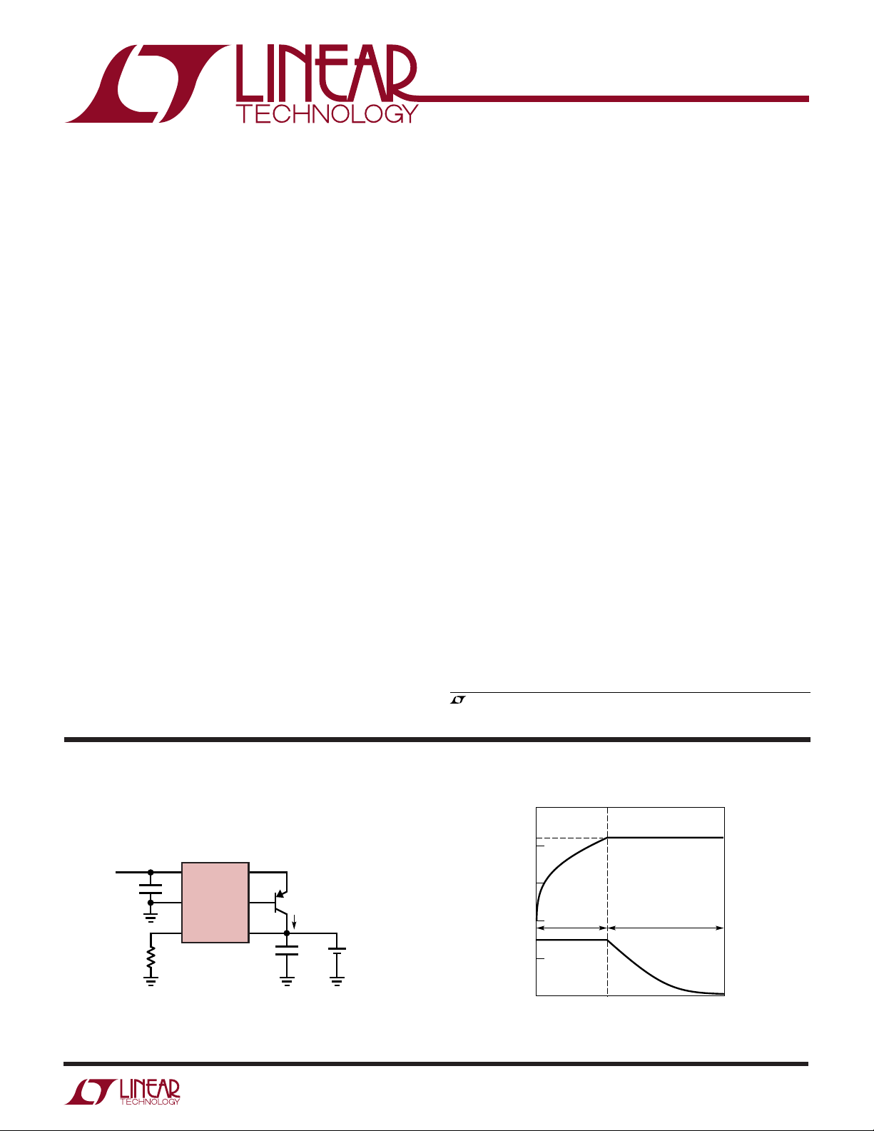
TYPICAL APPLICATIO
300mA Li-Ion Battery Charger
V
IN
5V
1µF
31
2
4
R
PROG
5k
V
CC
LTC1734
GND
PROG
I
SENSE
DRIVE
BAT
6
5
U
FMMT549
I
BAT
10µF
= 300mA
+
SINGLE
Li-Ion
BATTERY
1734 TA01
PROG Pin Indicates Charge Status
5V
V
(V)V
4V
BAT
V
3V
2V
1.5V
(V)
1V
PROG
0V
CHARGING
BEGINS
CONSTANT
CURRENT
BAT
V
CONSTANT
VOLTAGE
PROG
CHARGING
COMPLETE
1734 TA01b
1
Page 2
LTC1734
WW
W
ABSOLUTE MAXIMUM RATINGS
U
U
W
PACKAGE/ORDER INFORMATION
(Note 1)
Supply Voltage (VCC) ...................................–0.3V to 9V
Input Voltage (BAT, PROG) ........ –0.3V to (VCC + 0.3V)
Output Voltage (DRIVE) .............. –0.3V to (VCC + 0.3V)
Output Current (I
) ................................... –900mA
SENSE
Short-Circuit Duration (DRIVE) ...................... Indefinite
Junction Temperature.......................................... 125°C
Operating Ambient Temperature Range
(Note 2) ...............................................–40°C to 85°C
Operating Junction Temperature (Note 2) ............ 100°C
TOP VIEW
I
1
SENSE
GND 2
3
V
CC
S6 PACKAGE
6-LEAD PLASTIC SOT-23
T
= 125°C, θJA = 230°C/W
JMAX
6 DRIVE
5 BAT
4 PROG
ORDER PART
NUMBER
LTC1734ES6-4.1
LTC1734ES6-4.2
S6 PART MARKING
LTHD
LTRG
Storage Temperature Range ................. –65°C to 150°C
Lead Temperature (Soldering, 10 sec).................. 300°C
ELECTRICAL CHARACTERISTICS
temperature range, otherwise specifications are at TA = 25°C. VCC = 5V, GND = 0V and V
otherwise noted. All current into a pin is positive and current out of a pin is negative. All voltages are referenced to GND, unless
otherwise specified.
SYMBOL PARAMETER CONDITIONS MIN TYP MAX UNITS
VCC Supply
V
CC
I
CC
I
SHDN
I
BMS
I
BSL
V
UVLOI
V
UVLOD
V
UVHYS
Charging Performance
V
BAT
I
BAT1
I
BAT2
V
CM1
V
CM2
I
DSINK
Operating Supply Range (Note 5) ● 4.55 8 V
Quiescent VCC Pin Supply Current V
VCC Pin Supply Current in Manual Shutdown PROG Pin Open ● 450 900 µA
Battery Drain Current in Manual Shutdown PROG Pin Open ● –1 0 1 µA
(Note 3)
Battery Drain Current in Sleep Mode (Note 4) VCC = 0V ● –1 0 1 µA
Undervoltage Lockout Exit Threshold VCC Increasing ● 4.45 4.56 4.68 V
Undervoltage Lockout Entry Threshold VCC Decreasing ● 4.30 4.41 4.53 V
Undervoltage Lockout Hysteresis VCC Decreasing 150 mV
Output Float Voltage in Constant Voltage Mode 4.1V Version, I
Output Full-Scale Current When Programmed R
for 200mA in Constant Current Mode Pass PNP Beta > 50
Output Full-Scale Current When Programmed R
for 700mA in Constant Current Mode Pass PNP Beta > 50
Current Monitor Voltage on PROG Pin I
Current Monitor Voltage on PROG Pin I
Drive Output Current V
The ● denotes the specifications which apply over the full operating
= 5V, (Forces I
BAT
= 200µA,(7500Ω from PROG to GND)
I
PROG
4.2V Version, I
= 7500Ω, 4.55V ≤ VCC ≤ 8V, ● 155 200 240 mA
PROG
= 2143Ω, 4.55V ≤ VCC ≤ 8V, ● 620 700 770 mA
PROG
= 10% of I
BAT
4.55V ≤ V
≤ 85°C
0°C ≤ T
A
= 10% of I
BAT
4.55V ≤ V
0°C ≤ T
≤ 85°C
A
= 3.5V ● 30 mA
DRIVE
Consult LTC Marketing for parts specified with wider operating temperature ranges.
is equal to the float voltage unless
BAT
= I
DRIVE
= 10mA, 4.55V ≤ VCC ≤ 8V ● 4.059 4.10 4.141 V
BAT
= 10mA, 4.55V ≤ VCC ≤ 8V ● 4.158 4.20 4.242 V
BAT
, R
BAT1
BAT2
, R
PROG
PROG
≤ 8V, Pass PNP Beta > 50,
CC
≤ 8V, Pass PNP Beta > 50,
CC
= 0), ● 670 1150 µA
BAT
= 7500Ω, 0.045 0.15 0.28 V
= 2143Ω, 0.10 0.15 0.20 V
U
2
Page 3
LTC1734
TEMPERATURE (°C)
–50
190
I
BAT1
(mA)
200
210
0
50
75
1734 G03
–25
25
100
125
R
PROG
= 7.5k
PNP = FCX589
VCC = 4.55V AND 8V
ELECTRICAL CHARACTERISTICS
temperature range, otherwise specifications are at TA = 25°C. VCC = 5V, GND = 0V and V
The ● denotes the specifications which apply over the full operating
is equal to the float voltage unless
BAT
otherwise noted. All current into a pin is positive and current out of a pin is negative. All voltages are referenced to GND, unless
otherwise specified.
SYMBOL PARAMETER CONDITIONS MIN TYP MAX UNITS
Charger Manual Control
V
MSDT
V
MSHYS
I
PROGPU
Protection
I
DSHRT
Note 1: Absolute Maximum Ratings are those values beyond which the life
of a device may be impaired.
Note 2: The LTC1734E is guaranteed to meet performance specifications
from 0°C to 70°C ambient temperature range and 0°C to 100°C junction
temperature range. Specifications over the –40°C to 85°C operating
ambient temperature range are assured by design, characterization and
correlation with statistical process controls.
Note 3: Assumes that the external PNP pass transistor has negligible B-C
reverse-leakage current when the collector is biased at 4.2V (V
base is biased at 5V (V
Manual Shutdown Threshold V
Manual Shutdown Hysteresis V
Programming Pin Pull-Up Current V
Drive Output Short-Circuit Current Limit V
).
CC
Increasing ● 2.05 2.15 2.25 V
PROG
Decreasing from V
PROG
= 2.5V –6 –3 –1.5 µA
PROG
= V
DRIVE
CC
MSDT
● 35 65 130 mA
90 mV
Note 4: Assumes that the external PNP pass transistor has negligible B-E
reverse-leakage current when the emitter is biased at 0V (V
base is biased at 4.2V (V
BAT
).
CC
Note 5: The 4.68V maximum undervoltage lockout (UVLO) exit threshold
must first be exceeded before the minimum V
Short duration drops below the minimum V
specification applies.
CC
specification of several
CC
microseconds or less are ignored by the UVLO. If manual shutdown is
entered, then VCC must be higher than the 4.68V maximum UVLO
) and the
BAT
threshold before manual shutdown can be exited. When operating near the
minimum V
, a suitable PNP transistor with a low saturation voltage
CC
must be used.
) and the
UW
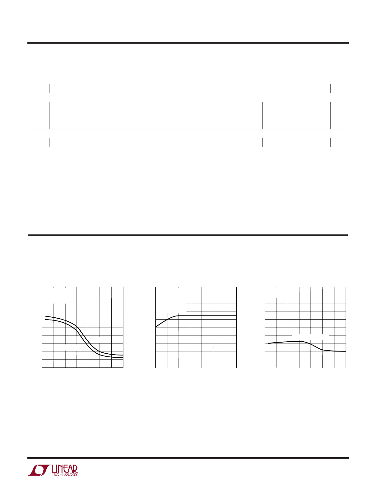
TYPICAL PERFOR A CE CHARACTERISTICS
Float Voltage vs Temperature
4.21
4.20
FLOAT VOLTAGE (V)
4.19
and Supply Voltage
I
= 10mA
BAT
PNP = FCX589
4.2V OPTION
V
= 4.55V
CC
25
–25
0
TEMPERATURE (°C)
–50
VCC = 8V
50
100
125
1734 G01
75
Float Voltage vs I
4.201
VCC = 5V
= 25°C
T
A
PNP = FCX589
4.2V OPTION
= 2150Ω
R
PROG
4.200
FLOAT VOLTAGE (V)
4.199
0
100
200
300
I
BAT
BAT
400
(mA)
500
600
1734 G02
700
I
vs Temperature
BAT1
and Supply Voltage
3
Page 4
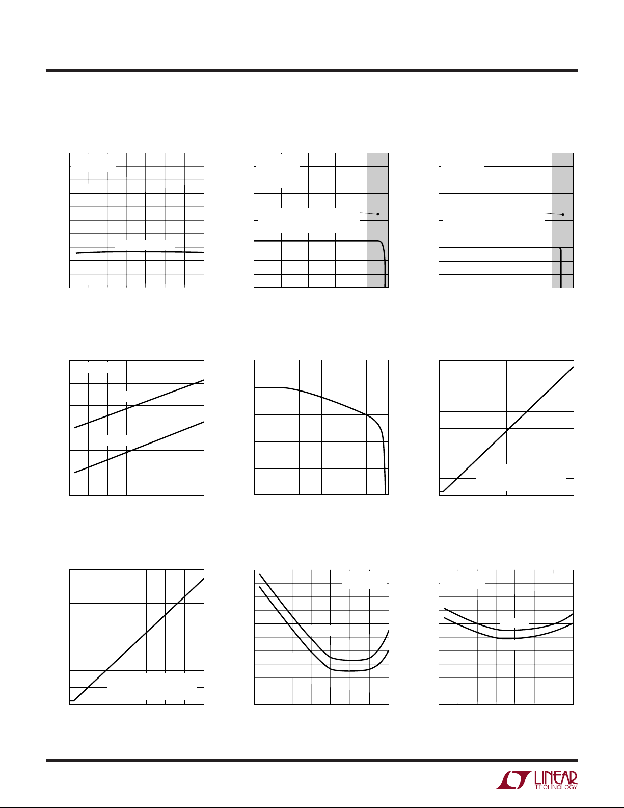
LTC1734
TEMPERATURE (°C)
–50
140
V
PROG
(mV)
150
160
0
50
75
1734 G12
–25
25
100
125
R
PROG
= 2.15k
PNP = FCX589
VCC = 8V
V
CC
= 4.55V
UW
TYPICAL PERFOR A CE CHARACTERISTICS
I
vs Temperature
BAT2
and Supply Voltage
740
R
= 2.15k
PROG
PNP = FCX589
I
210
vs V
BAT1
VCC = 5V
T
= 25°C
A
= 7.5k
R
PROG
PNP = FCX589
BAT
I
750
vs V
BAT2
VCC = 5V
T
= 25°C
A
= 2.15k
R
PROG
PNP = FCX589
BAT
(mA)
700
BAT2
I
VCC = 4.55V AND 8V
660
–50
0
–25
TEMPERATURE (°C)
50
25
Program Pin Pull-Up Current vs
Temperature and Supply Voltage
3.6
V
= 2.5V
PROG
3.5
V
= 8V
3.4
(µA)
3.3
PROGPU
I
3.2
3.1
3.0
–50
–25 0
CC
VCC = 4.55V
50 100 125
25 75
TEMPERATURE (°C)
BAT PIN MUST BE DISCONNECTED
(mA)
200
BAT1
I
100
125
1734 G04
75
190
AND GROUNDED TO FORCE
CC MODE IN THIS REGION
1
0
3
4
2
V
(V)
BAT
5
1734 G05
Program Pin Pull-Up Current
vs V
PROG
3.6
VCC = 8V
= 25°C
T
A
3.4
3.2
(µA)
PROGPU
3.0
I
2.8
1734 G07
2.6
2
456
3
V
PROG
(V)
78
1635 G08
BAT PIN MUST BE DISCONNECTED
(mA)
BAT2
I
700
650
AND GROUNDED TO FORCE
CC MODE IN THIS REGION
1
0
2
V
BAT
Program Pin Voltage
vs Charge Current (200mA)
1.6
VCC = 5V
T
= 25°C
A
(V)
PROG
V
1.4
1.2
1.0
0.8
0.6
0.4
0.2
R
PROG
PNP = FCX589
0
0
= 7.5k
LIMITS AT 25mV DUE TO
PROGRAMMING PIN PULL-UP
CURRENT (I
I
100
BAT1
50
(V)
PROGPU
(mA)
3
4
5
1734 G06
)
150
200
1734 F09
4
Program Pin Voltage
vs Charge Current (700mA)
1.6
VCC = 5V
= 25°C
T
A
1.4
1.2
1.0
(V)
0.8
PROG
V
0.6
0.4
0.2
= 2.15k
R
PROG
PNP = FCX589
LIMITS AT 6mV DUE TO
PROGRAMMING PIN PULL-UP
0
0
CURRENT (I
100 200 400
300
I
BAT2
PROGPU
(mA)
)
500 600 700
1734 G10
Program Pin Voltage for I
BAT1
vs Temperature and Supply Voltage
160
(mV)
150
PROG
V
140
–50
–25
V
CC
= 4.55V
0
VCC = 8V
25
TEMPERATURE (°C)
50
R
PROG
PNP = FCX589
75
/10
= 7.5k
100
1734 G11
125
Program Pin Voltage for I
BAT2
/10
vs Temperature and Supply Voltage
Page 5

UUU
PIN FUNCTIONS
I
(Pin 1): Sense Node for Charge Current. Current
SENSE
from VCC passes through the internal current sense resistor and reappears at I
external PNP emitter. The PNP collector provides charge
current to the battery.
GND (Pin 2): Ground. Provides a reference for the internal
voltage regulator and a return for all internal circuits.
When in the constant voltage mode, the LTC1734 will
precisely regulate the voltage between the BAT and GND
pins. The battery ground should connect close to the GND
pin to avoid voltage drop errors.
VCC (Pin 3): Positive Input Supply Voltage. This pin
supplies power to the internal control circuitry and external PNP transistor through the internal current sense
resistor. This pin should be bypassed to ground with a
capacitor in the range of 1µF to 10µF.
PROG (Pin 4): Charge Current Programming, Charge
Current Monitor and Manual Shutdown Pin. Provides a
virtual reference voltage of 1.5V for an external resistor
(R
) tied between this pin and ground that programs
PROG
the battery charge current when the charger is in the
constant current mode. The typical charge current will be
1000 times greater than the current through this resistor
to supply current to the
SENSE
LTC1734
(I
= 1500/R
BAT
current to be monitored. The voltage on this pin is proportional to the charge current where 1.5V corresponds to the
full programmed currrent. Floating this pin allows an
internal current source to pull the pin voltage above the
shutdown threshold voltage. Because this pin is in a signal
path, excessive capacitive loading can cause AC instability. See the Applications Information section for more
details.
BAT (Pin 5): Battery Voltage Sense Input. A precision
internal resistor divider sets the final float voltage on this
pin. This divider is disconnected in the manual shutdown
or sleep mode. When charging, approximately 34µA
flows into the BAT pin. To minimize float voltage errors,
avoid excessive resistance between the battery and the
BAT pin. For dynamically stable operation, this pin usually
requires a minimum bypass capacitance to ground of 5µF
to frequency compensate for the high frequency inductive
effects of the battery and wiring.
DRIVE (Pin 6): Base Drive Output for the External PNP
Pass Transistor. Provides a controlled sink current that
drives the base of the PNP. This pin has current limiting
protection for the LTC1734.
). This pin also allows for the charge
PROG
BLOCK DIAGRA
VOLTAGE
REFERENCE
2.5V
UVLO
2.15V
C1
+
–
W
REF
SHUTDOWN
SHUTDOWN
V
IN
1µF
V
CC
3
I
/1000
BAT
60Ω 0.06Ω
1.5V
3µA
4
PROG
R
PROG
I
BAT
SHUTDOWN
+
–
A3
+
–
OUTPUT
DRIVER
TEMPERATURE AND
CURRENT LIMITING
A1A2
SHUTDOWN
2.5V
+
–
I
SENSE
1
DRIVE
6
I
BAT
BAT
5
10µF
1734 BD
2
GND
SINGLE
Li-Ion
CELL
5
Page 6

LTC1734
OPERATIO
U
The LTC1734 is a linear battery charger controller. Operation can best be understood by referring to the Block
Diagram. Charging begins when VCC rises above the
UVLO (Undervoltage Lockout) threshold V
external current programming resistor is connected between the PROG pin and ground. When charging, the
collector of the external PNP provides the charge current.
The PNP’s emitter current flows through the I
and through the internal 0.06Ω current sense resistor.
This current is close in magnitude, but slightly more than
the collector current since it includes the base current.
Amplifier A3, along with the P-channel FET, will force the
same voltage that appears across the 0.06Ω resistor to
appear across the internal 60Ω resistor. The scale factor
of 1000:1 in resistor values will cause the FET’s drain
current to be 1/1000 of the charge current and it is this
current that flows through the PROG pin. In the constant
current mode, amplifier A2 is used to limit the charge
current to the maximum that is programmed by R
The PROG pin current, which is 1/1000 of the charge
current, develops a voltage across the program resistor.
When this voltage reaches 1.5V, amplifier A2 begins
diverting current away from the output driver, thus limiting the charge current. This is the constant current mode.
The constant charge current is 1000 • (1.5V/R
As the battery accepts charge, its voltage rises. When it
reaches the preset float voltage of 4.2V (LTC1734-4.2
version), a precisely divided down version of this voltage
(2.5V) is compared to the 2.5V internal reference voltage
by amplifier A1. If the battery voltage attempts to exceed
UVLOI
SENSE
PROG
and an
pin
PROG
).
.
4.2V (2.5V at amplifier A1’s input) the amplifier will divert
current away from the output driver thus limiting charge
current to that which will maintain 4.2V on the battery. This
is the constant voltage mode.
When in the constant voltage mode, the 1000:1 current
ratio is still valid and the voltage on the PROG pin will
indicate the charge current as a proportion of the maximum current set by the current programming resistor.
The battery charge current is 1000 • (V
This feature allows a microcontroller with an ADC to easily
monitor charge current and if desired, manually shut down
the charger at the appropriate time.
When VCC is applied, the charger can be manually shut
down by floating the otherwise grounded end of R
An internal 3µA current source pulls the PROG pin above
the 2.15V threshold of voltage comparator C1 initiating
shutdown.
For charging NiMH or NiCd batteries, the LTC1734 can
function as a constant current source by grounding the
BAT pin. This will prevent amplifier A1 from trying to limit
charging current and only A2 will control the current.
Fault conditions such as overheating of the die or excessive DRIVE pin current are monitored and limited.
When input power is removed or manual shutdown is
entered, the charger will drain only tiny leakage currents
from the battery, thus maximizing battery standby time.
With VCC removed the external PNP’s base is connected to
the battery by the charger. In manual shutdown the base
is connected to VCC by the charger.
PROG/RPROG
) amps.
PROG
.
WUUU
APPLICATIO S I FOR ATIO
Charging Operation
Charging begins when an input voltage is present that
exceeds the undervoltage lockout threshold (V
Li-Ion battery is connected to the charger output and a
program resistor is connected from the PROG pin to
ground. During the first portion of the charge cycle, when
the battery voltage is below the preset float voltage, the
charger is in the constant current mode. As the battery
voltage rises and reaches the preset float voltage, the
UVLOI
), a
6
charge current begins to decrease and the constant
voltage portion of the charge cycle begins. The charge
current will continue to decrease exponentially as the
battery approaches a fully charged condition.
Should the battery be removed during charging, a fast
built-in protection circuit will prevent the BAT pin from rising above 5V, allowing the precision constant voltage
circuit time to respond.
Page 7

LTC1734
U
WUU
APPLICATIONS INFORMATION
Manual Shutdown
Floating the program resistor allows an internal 3µA
current source (I
PROGPU
2.15V shutdown threshold (V
the charger. In this mode, the LTC1734 continues to draw
some current from the supply (I
gible leakage current is delivered to the battery (I
Shutdown can also be accomplished by pulling the otherwise grounded end of the program resistor to a voltage
greater than 2.25V (V
1.5V, but the internal battery voltage resistor divider will
draw about 34µA from the battery until shutdown is
entered. Figure 1 illustrates a microcontroller configuration that can either float the resistor or force it to a voltage.
The voltage should be no more than 8V when high and
have an impedance to ground of less than 10% of the
program resistor value when low to prevent excessive
charge current errors. To reduce errors the program
resistor value may be adjusted to account for the impedance to ground. The programming resistor will prevent
potentially damaging currents if the PROG pin is forced
above VCC. Under this condition VCC may float, be loaded
down by other circuitry or be shorted to ground. If V
not shorted to ground the current through the resistor will
pull V
up somewhat.
CC
) to pull the PROG pin above the
), thus shutting down
MSDT
), but only a negli-
SHDN
BMS
Max). Charging will cease above
MSDT
).
CC
is
entering shutdown, but no more than 0.3V above V
CC
to
prevent damaging the LTC1734 from excessive PROG
pin current. An exception is if VCC is allowed to float with
no other circuitry loading VCC down. Then, because the
current will be low, it is allowable to have the PROG pin
shutdown voltage applied. A three-state logic driver with
sufficient pull-up current can be used to perform this
function by enabling the high impedance state to charge
or enabling the pull-up device to enter shutdown.
An NPN transistor or a diode can also be utilized to
implement shutdown from a voltage source. These have
the advantage of blocking current when the voltage source
goes low, thus automatically disconnecting the voltage
source for normal charging operation. The use of an NPN
allows for use of a weak voltage source due to the current
gain of the transistor. For an NPN connect the collector to
V
the base to the voltage source and the emitter to the
CC,
PROG pin. For a diode, connect the anode to the voltage
source and cathode to the PROG pin. An input high level
ranging from 3.3V to VCC should be adequate to enter
shutdown while a low level of 0.5V or less should allow for
normal charging operation. Use of inexpensive small
signal devices such as the 2N3904 or 1N914 is recommended to prevent excessive capacitive loading on the
PROG pin (see Stability section).
Another method is to directly switch the PROG pin to a
voltage source when shutdown is desired (Caution: pulling the PROG below 1.5V with VCC applied will cause
excessive and uncontrolled charge currents). The voltage source must be capable of sourcing the resulting
current through the program resistor. This has the advantage of not adding any error to the program resistor
during normal operation. The voltage on the PROG pin
must be greater than 2.25V (V
R
OPEN DRAIN
OR TOTEM
POLE OUTPUT
µC
ADC INPUT
Figure 1. Interfacing with a Microcontroller
PROG
MSDT(MAX)
PROG
LTC1734
) to ensure
1734 F01
Sleep Mode
When the input supply is disconnected, the IC enters the
sleep mode. In this mode, the battery drain current (I
BSL
)
is a negligible leakage current, allowing the battery to remain connected to the charger for an extended period of
time without discharging the battery. The leakage current
is due to the reverse-biased B-E junction of the external
PNP transistor.
Undervoltage Lockout
Undervoltage lockout (UVLO) keeps the charger off until
the input voltage exceeds a predetermined threshold level
(V
) that is typically 4.56V. Approximately 150mV of
UVLOI
hysteresis is built in to prevent oscillation around the
threshold level. In undervoltage lockout, battery drain
current is very low (<1µA).
7
Page 8

LTC1734
U
WUU
APPLICATIONS INFORMATION
Programming Constant Current
When in the constant current mode, the full-scale charge
current (C) is programmed using a single external resistor
between the PROG pin and ground. This charge current
will be 1000 times greater than the current through the
program resistor. The program resistor value is selected
by dividing the voltage forced across the resistor (1.5V)
by the desired resistor current.
The LTC1734 is designed for a maximum current of
approximately 700mA. This translates to a maximum
PROG pin current of 700µA and a minimum program
resistor of approximately 2.1k. Because the PROG pin is in
a closed-loop signal path, the pole frequency must be kept
high enough to maintain adequate AC stability by avoiding
excessive capacitance on the pin. See the Stability section
for more details.
The minimum full-scale current that can be reliably programmed is approximately 50mA, which requires a program resistor of 30k. Limiting capacitive loading on the
program pin becomes more important when high value
program resistors are used. In addition, the current
monitoring accuracy can degrade considerably at very
low current levels. If current monitoring is desired, a
minimum full-scale current of 200mA is recommended.
Different charge currents can be programmed by various
means such as by switching in different program resistors
as shown in Figures 2 and 3. A voltage DAC connected
through a resistor to the PROG pin or a current DAC
connected in parallel with a resistor to the PROG pin can
also be used to program current (the resistor is required
with the I
to maintain AC stability as discussed in the
DAC
Stability section). Another means is to use a PWM output
from a microcontroller to duty cycle the charger into and
out of shutdown to create an average current (see Manual
Shutdown section for interfacing examples). Because
chargers are generally slow to respond, it can take up to
approximately 300µs for the charger to fully settle after a
shutdown is deasserted. This delay must be accounted for
unless the minimum PWM low duration is about 3ms or
more. Shutdown occurs within a few microseconds of a
shutdown command. The use of PWM can extend the
average current to less than the normal 200mA minimum
constant current.
CHARGE
CURRENT
MONITOR
(FILTERED)
OPTIONAL FILTER
1k
0.1µF TO
0.5µF
Figure 2. Logic Control Programming of Output Current to 0mA, 200mA, 500mA or 700mA
PIN 4
CONTROL 1
CHARGE
CURRENT
MONITOR
(UNFILTERED)
V
IN
5V
1µF
3k
Q1
2N7002
CONTROL 2
V
IN
5V
1µF
3k
Q1
2N7002
CONTROL 1
Q2
2N7002
CONTROL 2
31
2
4
7.5k
V
CC
LTC1734
GND
PROG
I
SENSE
6
DRIVE
5
BAT
*OBSERVE MAXIMUM TEMPERATURE
31
2
4
7.5k
Q2
2N7002
V
CC
GND
PROG
I
SENSE
LTC1734
DRIVE
FZT549*
LOAD
BAT
I
LOAD
1734 F03
6
5
FZT549
I
BAT
10µF
CURRENT
0
200mA
500mA
700mA
CHARGE CURRENT
SINGLE
Li-Ion
BATTERY
1734 F02
CONTROL 1
LOW
LOW
HIGH
HIGH
0
200mA
500mA
700mA
CONTROL 2
LOW
HIGH
LOW
HIGH
CONTROL 1
LOW
LOW
HIGH
HIGH
CONTROL 2
LOW
HIGH
LOW
HIGH
8
Figure 3. Programmable Current Source with Output Current of 0mA, 200mA, 500mA or 700mA
Page 9

LTC1734
U
WUU
APPLICATIONS INFORMATION
Monitoring Charge Current
The voltage on the PROG pin indicates the charge current
as a proportion of the maximum current set by the
program resistor. The charge current is equal to 1000 •
(V
PROG/RPROG
ler with an ADC to easily monitor charge current and if
desired, manually shut down the charger at the appropriate time. See Figure 1 for an example. The minimum PROG
pin current is about 3µA (I
Errors in the charge current monitor voltage on the PROG
pin are inversely proportional to battery current and can be
statistically approximated as follows:
One Sigma Error(%) ≅ 1 + 0.3/I
Dynamic loads on the battery will cause transients to
appear on the PROG pin. Should they cause excessive
errors in charge current monitoring, a simple RC filter as
shown in Figure 2 can be used to filter the transients. The
filter will also quiet the PROG pin to help prevent inadvertent momentary entry into the manual shutdown mode.
Because the PROG pin is in a closed-loop signal path the
pole frequency must be kept high enough to maintain
adequate AC stability. This means that the maximum
resistance and capacitance presented to the PROG pin
must be limited. See the Stability section for more details.
Constant Current Source
The LTC1734 can be used as a constant current source by
disabling the voltage control loop as shown in Figure 3.
This is done by pulling the BAT pin below the preset float
voltages of 4.1V or 4.2V by grounding the BAT pin. The
program resistor will determine the output current. The
output current range can be between approximately 50mA
and 700mA, depending on the maximum power rating of
the external PNP pass transistor.
External PNP Transistor
The external PNP pass transistor must have adequate
beta, low saturation voltage and sufficient power dissipation capability (including any heat sinking, if required).
) amps. This feature allows a microcontrol-
PROGPU
).
BAT
(A)
used, more base current is required from the LTC1734.
This can result in the output drive current limit being
reached, or thermal shutdown due to excessive power
dissipation. Excessive beta can affect AC stability (see
Stability section)
With low supply voltages, the PNP saturation voltage
(V
than the minimum supply voltage minus the maximum
voltage drop across the internal sense resistor and bond
wires (0.1Ω) and battery float voltage. If the PNP transistor can not achieve the low saturation voltage required,
base current will dramatically increase. This is to be
avoided for a number of reasons: output drive may reach
current limit resulting in the charger’s characteristics to
go out of specifications, excessive power dissipation may
force the IC into thermal shutdown, or the battery could
become discharged because some of the current from the
DRIVE pin could be pulled from the battery through the
forward biased collector base junction.
For example, to program a charge current of 500mA with
a minimum supply voltage of 4.75V, the minimum operating VCE is:
The actual battery charge current (I
than the expected charge current because the charger
senses the emitter current and the battery charge current
will be reduced by the base current. In terms of β (IC/IB),
I
BAT
If β = 50, then I
be compensated for by increasing I
Another important factor to consider when choosing the
PNP pass transistor is the power handling capability. The
transistor’s data sheet will usually give the maximum rated
power dissipation at a given ambient temperature with a
power derating for elevated temperature operation. The
maximum power dissipation of the PNP when charging is:
) becomes important. The V
CESAT
V
CE(MIN)
can be calculated as follows:
I
BAT
P
D(MAX)
(V) = 4.75 – (0.5)(0.1) – 4.2 = 0.5V
(A) = 1000 • I
BAT
(W) = I
BAT (VDD(MAX)
[β/(β + 1)]
PROG
is 2% low. If desired, the 2% loss can
must be less
CESAT
) is slightly smaller
BAT
by 2%.
PROG
– V
BAT(MIN)
)
To provide 700mA of charge current with the minimum
available base drive of approximately 30mA requires a
PNP beta greater than 23. If lower beta PNP transistors are
V
DD(MAX)
the minimum battery voltage when discharged.
is the maximum supply voltage and V
BAT(MIN)
is
9
Page 10

LTC1734
U
WUU
APPLICATIONS INFORMATION
Table 1. PNP Pass Transistor Selection Guide
Maximum PD (W)
Mounted on Board
= 25°C Package Style ZETEX Part Number ROHM Part Number Comments
at T
A
0.5 SOT-23 FMMT549 Low V
0.625 SOT-23 FMMT720 Very Low V
1 SOT-89 FCX589 or BCX69
1.1 SOT-23-6 ZXT10P12DE6 Very Low V
1 to 2 SOT-89 FCX717 Very Low V
2 SOT-223 FZT589 Low V
2 SOT-223 BCP69 or FZT549
0.75 FTR 2SB822 Low V
1 ATV 2SB1443 Low V
2 SOT-89 2SA1797 Low V
10 (TC = 25°C) TO-252 2SB1182 Low V
Once the maximum power dissipation and V
CE(MIN)
known, Table 1 can be used as a guide in selecting some
PNPs to consider. In the table, very low V
0.25V, low V
is 0.25V to 0.5V and the others are 0.5V
CESAT
CESAT
is less than
to 0.8V all depending on the current. See the manufacturer’s
data sheet for details. All of the PNP transistors are rated
to carry at least 1A continuously as long as the power
dissipation is within limits. The Stability section addresses
caution in the use of high beta PNPs.
Should overheating of the PNP transistor be a concern,
protection can be achieved with a positive temperature
coefficient (PTC) thermistor, wired in series with the
current programming resistor and thermally coupled to
the transistor. The PTH9C chip series from Murata has a
steep resistance increase at temperature thresholds from
85°C to 145°C making it behave somewhat like a thermostat switch. For example, the model PTH9C16TBA471Q
thermistor is 470Ω at 25°C, but abruptly increase its
resistance to 4.7k at 125°C. Below 125°C, the device
exhibits a small negative TC. The 470Ω thermistor can be
added in series with a 1.6k resistor to form the current
programming resistor for a 700mA charger. Should the
thermistor reach 125°C, the charge current will drop to
238mA and inhibit any further increase in temperature.
are
CESAT
High Beta
CESAT,
High Beta, Small
CESAT,
High Beta
CESAT,
CESAT
CESAT
CESAT
CESAT
High Beta
CESAT,
constant voltage mode, a capacitor of at least 4.7µF is
usually required from BAT to ground. The battery and
interconnecting wires appear inductive at high frequencies, and since these are in the feedback loop, this capacitance may be necessary to compensate for the inductance.
This capacitor need not exceed 100µF and its ESR can
range from near zero to several ohms depending on the
inductance to be compensated. In general, compensation
is optimal with a capacitance of 4.7µF to 22µF and an ESR
of 0.5Ω to 1.5Ω.
Using high beta PNP transistors (>300) and very low ESR
output capacitors (especially ceramic) reduces the phase
margin, possibly resulting in oscillation. Also, using high
value capacitors with very low ESRs will reduce the phase
margin. Adding a resistor of 0.5Ω to 1.5Ω in series with
the capacitor will restore the phase margin.
In the constant current mode, the PROG pin is in the
feedback loop, not the battery. Because of this, capacitance on this pin must be limited. Locating the program
resistor near the PROG pin and isolating the charge
current monitoring circuitry (if used) from the PROG pin
with a 1k to 10k resistor may be necessary if the capacitance is greater than that given by the following equation:
Stability
The LTC1734 contains two control loops: constant voltage
and constant current. To maintain good AC stability in the
10
C
MAX pF
()
k
400
=
R
PROG
Page 11

LTC1734
V
CC
V
IN
*
1734 F06
LTC1734
*DRAIN-BULK DIODE OF FET
U
WUU
APPLICATIONS INFORMATION
Higher charge currents require lower program resistor
values which can tolerate more capacitive loading on the
PROG pin. Maximum capacitance can be as high as 50pF
for a charge current of 200mA (R
Figure 4 is a simple test circuit for checking stability in both
the constant current and constant voltage modes. With
input power applied and a near fully charged battery
connected to the charger, driving the PROG pin with a
pulse generator will cycle the charger in and out of the
manual shutdown mode. Referring to Figure 5, after a
short delay, the charger will enter the constant current
mode first, then if the battery voltage is near the programmed voltage of 4.1V or 4.2V, the constant voltage
mode will begin. The resulting waveform on the PROG pin
is an indication of stability.
The double exposure photo in Figure 5 shows the effects
of capacitance on the program pin. The middle waveform
is typical while the lower waveform indicates excessive
program pin capacitance resulting in constant current
mode instability. Although not common, ringing on the
constant voltage portion of the waveform is an indication
PROG
= 7.5k).
of instability due to any combination of extremely low ESR
values, high capacitance values of the output capacitor or
very high PNP transistor beta. To minimize the effect of the
scope probe capacitance, a 10k resistor is used to isolate
the probe from the program pin. Also, an adjustable load
resistor or current sink can be used to quickly alter the
charge current when a fully charged battery is used.
Reverse Input Voltage Protection
In some applications, protection from reverse voltage on
VCC is desired. If the supply voltage is high enough, a
series blocking diode can be used. In other cases, where
the voltage drop must be kept low, a P-channel FET as
shown in Figure 6 can be used.
Figure 6. Low Loss Reverse Voltage Protection
VCC Bypass Capacitor
TO SCOPE
2.5V
GENERATOR
(20pF ON PIN)
(200pF ON PIN)
10k
R
PROG
3k
0V
f = 1kHz
Figure 4. Setup for AC Stability Testing
5V
PULSE
0V
2V
PROG PIN
PROG PIN
1V
0V
2V
1V
0V
SHUT
DOWN
Figure 5. Stability Waveforms
PROG
*FULLY CHARGED CELL
DELAY CONSTANT
HORIZONTAL SCALE: 100µs/DIV
BAT
LTC1734
CURRENT
Information furnished by Linear Technology Corporation is believed to be accurate and reliable.
However, no responsibility is assumed for its use. Linear Technology Corporation makes no representation that the interconnection of its circuits as described herein will not infringe on existing patent rights.
+
1734 F04
Li-Ion*
CONSTANT
VOLTAGE
6Ω TO
20Ω
Many types of capacitors with values ranging from 1µF to
10µF located close to the LTC1734 will provide adequate
input bypassing. However, caution must be exercised
when using multilayer ceramic capacitors. Because of the
self resonant and high Q characteristics of some types of
ceramic capacitors, high voltage transients can be generated under some start-up conditions, such as connecting
the charger input to a hot power source. To prevent these
transients from exceeding the absolute maximum voltage
rating, several ohms of resistance can be added in series
with the ceramic input capacitor.
Internal Protection
Internal protection is provided to prevent excessive DRIVE
pin currents (I
) and excessive self-heating of the
DSHRT
LTC1734 during a fault condition. The faults can be
generated from a shorted DRIVE pin or from excessive
DRIVE pin current to the base of the external PNP
transistor when it’s in deep saturation from too low a VCE.
This protection is not designed to prevent overheating of
the external pass transistor. Indirectly though, self-heating
of the PNP thermally conducting to the LTC1734 and
11
Page 12

LTC1734
U
WUU
APPLICATIONS INFORMATION
resulting in the IC’s junction temperature to rise above
150°C, thus cutting off the PNP’s base current. This
action will limit the PNP’s junction temperature to some
temperature well above 150°C. The temperature
U
PACKAGE DESCRIPTIO
S6 Package
6-Lead Plastic SOT-23
(LTC DWG # 05-08-1634)
(LTC DWG # 05-08-1636)
.20
(.008)
DATUM ‘A’
L
NOTE:
1. CONTROLLING DIMENSION: MILLIMETERS
2. DIMENSIONS ARE IN
3. DRAWING NOT TO SCALE
4. DIMENSIONS ARE INCLUSIVE OF PLATING
5. DIMENSIONS ARE EXCLUSIVE OF MOLD FLASH AND METAL BURR
6. MOLD FLASH SHALL NOT EXCEED .254mm
7. PACKAGE EIAJ REFERENCE IS:
SC-74A (EIAJ) FOR ORIGINAL
JEDEL MO-193 FOR THIN
MILLIMETERS
(INCHES)
.09 – .20
(.004 – .008)
(NOTE 2)
A2
A
(.074)
SOT-23
(Original)
.90 – 1.45
A
(.035 – .057)
.00 – 0.15
A1
(.00 – .006)
.90 – 1.30
A2
(.035 – .051)
.35 – .55
L
(.014 – .021)
depends on how well the IC and PNP are thermally
connected and on the transistor’s θJA. See the External
PNP Transistor section for information on protecting the
transistor from overheating.
2.80 – 3.10
(.110 – .118)
(NOTE 3)
1.90
REF
SOT-23
(ThinSOT)
1.00 MAX
(.039 MAX)
.01 – .10
(.0004 – .004)
.80 – .90
(.031 – .035)
.30 – .50 REF
(.012 – .019 REF)
A1
2.60 – 3.00
(.102 – .118)
1.50 – 1.75
(.059 – .069)
(NOTE 3)
.95
(.037)
REF
PIN ONE ID
.25 – .50
(.010 – .020)
(6PLCS, NOTE 2)
S6 SOT-23 0401
RELATED PARTS
PART NUMBER DESCRIPTION COMMENTS
LT®1510-5 500kHz Constant-Current/Constant-Voltage Battery Charger Up to 1A Charge Current for Li-Ion, NiCd, NiMH or Lead-Acid
LT1571-1/LT1571-2 200kHz/500kHz Constant-Current/Constant-Voltage Battery Up to 1.5A Charge Current for 1-, 2- or Multiple Cell Li-Ion Batteries,
LT1571-5 Charger Family Preset and Adjustable Battery Voltages, C/10 Charge Detection
LTC1729 Li-Ion Battery Charger Termination Controller Can be Used with LTC Battery Chargers to Provide Charge Termina-
LTC1730 Li-Ion Battery Pulse Charger Minimizes Heat Dissipation, No Blocking Diode Required,
LTC1731 Linear Constant-Current/Constant-Voltage Charger Controller Simple Charger Uses External FET. Features Preset Voltages,
LTC1732 Linear Constant-Current/Constant-Voltage Charger Controller Simple Charger Uses External FET. Input Power Good Indication
LT1769 200kHz Constant-Current/Constant-Voltage Battery Charger Up to 2A Charge Current for Li-Ion, NiCd, NiMH or Lead-Acid
Linear Technology Corporation
12
1630 McCarthy Blvd., Milpitas, CA 95035-7417
(408) 432-1900 ● FAX: (408) 434-0507
●
www.linear.com
Batteries
tion, Preset Voltages, C/10 Charge Detection and Timer Functions
Limits Maximum Current for Safety
C/10 Charge Detection and Programmable Timer
Features Preset Voltages, C/10 Charge Detection and Programmable Timer
Batteries with Input Current Limit
sn1734 1734fs LT/TP 0801 2K • PRINTED IN THE USA
LINEAR TECHNOLOGY CORPO RATION 2001
 Loading...