

Page 1

FEATURES
■
Two 0.4Ω/300mA N-Channel Switches
■
Available in MS8 and SO-8 Packages
■
SMBus and I2C Compatible
■
0.6V VIL and 1.4V VIH for DATA and CLK
■
Low Standby Current: 14µA
■
Separate Drain Connection to SW0
■
Three Addresses from One Three-State Address Pin
■
Independent Control of Up to Six Switches
■
Built-In Power-On Reset Timer
■
Built-In Undervoltage Lockout
LTC1710
SMBus Dual Monolithic
High Side Switch
U
DESCRIPTION
The LTC®1710 SMBus dual switch has two built-in 0.4Ω/
300mA switches that are controlled by a 2-wire SMBus
interface. With a low standby current of 14µ A (3.3V), the
LTC1710 operates over an input voltage range of 2.7V to
5.5V while maintaining the SMBus specified 0.6V VIL and
1.4V VIH input thresholds.
Using the 2-wire interface, CLK and DATA, the LTC1710
follows SMBus’s Send Byte Protocol to independently
control the two 0.4Ω internal N-channel power switches,
which are fully enhanced by onboard charge pumps.
U
APPLICATIONS
■
Handheld Computer Power Management
■
Computer Peripheral Control
■
Laptop Computer Power Plane Switching
■
Portable Equipment Power Control
■
Industrial Control Systems
■
ACPI SMBus Interface
U
TYPICAL APPLICATION
V
CC
2.7V TO 5.5V
81
SW0
5
CLOCK
FROM SMBus
(PROGRAMMABLE)
DATA
AD1
CHARGE
6
PUMP
3
SW1
LTC1710
SW0D
0V TO V
4
CC
2
7
10µF10µF
LOAD 1
LOAD 2
1710 TA01
The LTC1710 has one three-state programmable
address pin that allows three different addresses for a total
of six available switches on the same bus. The LTC1710
also features a separate user-controlled drain supply
(SW0D) to Switch 0 so that it can be used to control
SMBus peripherials using a different power supply.
, LTC and LT are registered trademarks of Linear Technology Corporation.
Switch Voltage Drop
vs Load Current
500
T
= 25°C
A
400
300
200
100
SWITCH VOLTAGE DROP (mV)
0
100
0
LOAD CURRENT (mA)
200
VCC = 2.7V
V
CC
= 5V
V
CC
300
= 3.3V
400
1710 TA02
1
Page 2
LTC1710
WW
W
U
ABSOLUTE MAXIMUM RATINGS
(Voltages Referred to GND Pin) (Note 1)
Input Supply Voltage (VCC).......................... –0.3V to 6V
Input Supply Voltage (VCC) with SW0 Connected
as a Low Side Switch ........................... – 0.3V to 3.6V
DATA, CLK (Bus Pins 6, 5)......................... –0.3V to 6V*
AD1 ( Address Pin 3) ....................... –0.3V to VCC + 0.3V
OUT0, OUT1 (Output Pins 2, 7) ................... – 0.3V to 6V
SW0D (Switch 0 Drain Pin 1)....................... –0.3V to 6V
OUT0, OUT1 (Output Pins 2, 7)
Continuous .................................................... 300mA
Pulsed, <10µ s (nonrepetitive) ............................... 1A
U
W
U
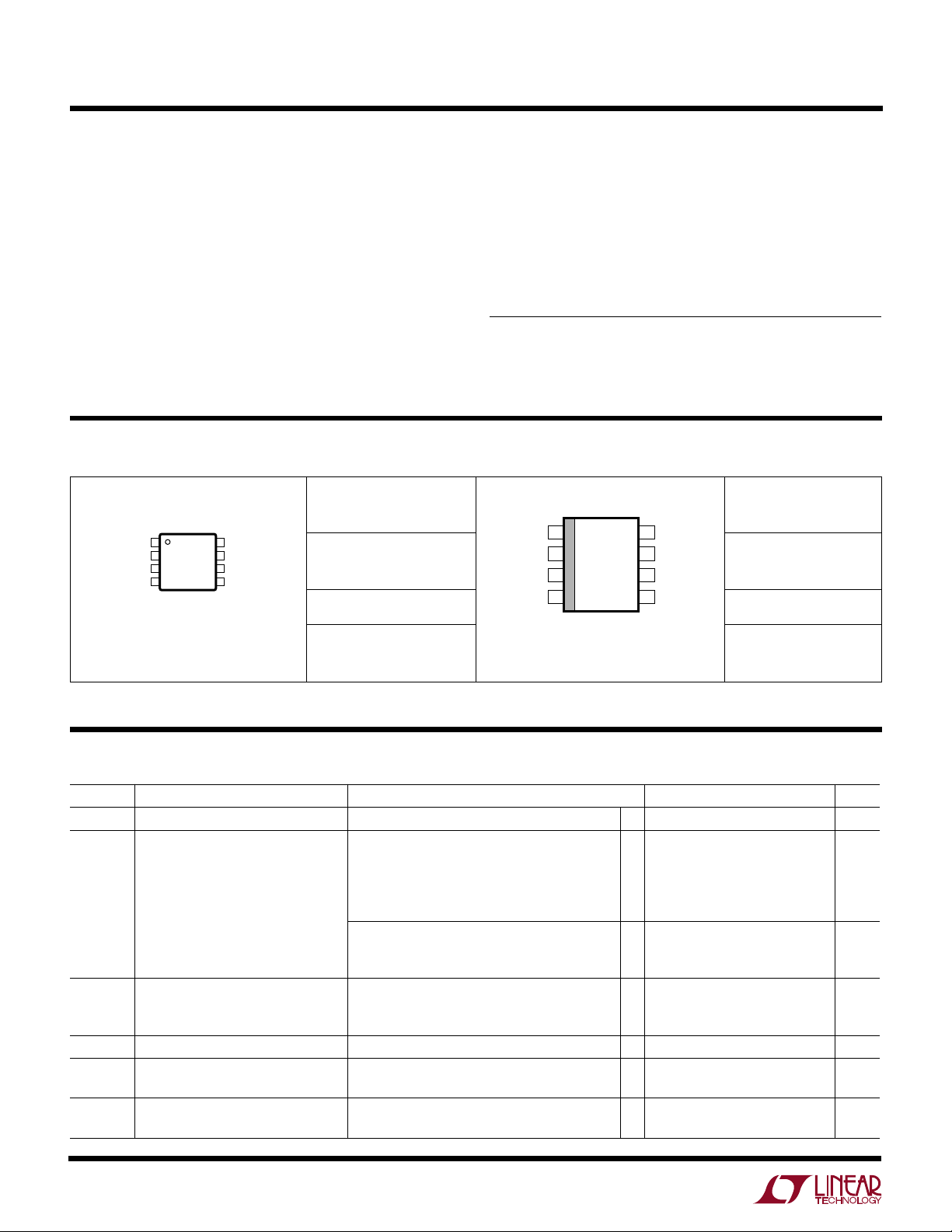
PACKAGE/ORDER INFORMATION
ORDER PART
TOP VIEW
SW0D
1
OUT0
2
AD1
3
GND
4
MS8 PACKAGE
8-LEAD PLASTIC MSOP
T
= 110°C, θJA = 150°C/W
JMAX
8
7
6
5
V
CC
OUT1
DATA
CLK
NUMBER
LTC1710CMS8
MS8 PART MARKING
LTDZ
Operating Temperature Range
LTC1710C................................................ 0°C to 70°C
LTC1710I ............................................ – 40°C to 85°C
Junction Temperature** ...................................... 125°C
Storage Temperature Range .................. –65°C to 150°C
Lead Temperature (Soldering, 10 sec)................... 300°C
*Supply rails to DATA and CLK are independent of VCC to LTC1710.
**Although the LTC1710 can sustain T
circuitry is set to shut down the switches at T
TOP VIEW
SW0D
1
OUT0
2
AD1
3
GND
4
= 125°C without damage, its internal protection
JMAX
= 120°C with 15°C hysteresis.
J
ORDER PART
NUMBER
V
8
CC
OUT1
7
DATA
6
CLK
5
LTC1710CS8
LTC1710IS8
S8 PART MARKING
S8 PACKAGE
8-LEAD PLASTIC SO
T
= 110°C, θJA = 110°C/W
JMAX
1710
1710I
Consult factory for Military grade parts.
ELECTRICAL CHARACTERISTICS
SYMBOL PARAMETER CONDITIONS MIN TYP MAX UNITS
V
CC
I
VCC
R
DS(ON)
V
UVLO
t
POR
f
OSC
Operating Supply Voltage Range ● 2.7 5.5 V
Supply Current Charge Pump Off, AD1 High or Low,
DATA and CLK High
V
CC
V
CC
V
CC
OUT0 or OUT1 High
(Command Byte XXXXXX01 or XXXXXX10) ● 200 300 µA
Both Outputs High (Command Byte XXXXXX11)
Power Switch On Resistance VCC = 2.7V, I
= 3.3V, I
V
CC
= 5V, I
V
CC
Undervoltage Lockout Falling Edge (Note 2) ● 1.5 2.0 2.5 V
Power-On Reset Delay Time VCC = 2.7V (Note 3) 300 1000 µs
= 5.5V 300 1000 µs
V
CC
Charge Pump Oscillator Frequency 300 kHz
(Note 3)
TA = 25°C, VCC = SW0D = 5V unless otherwise noted.
= 5V ● 17 30 µA
= 3.3V ● 14 30 µA
= 2.7V ● 11 30 µA
● 250 500 µA
= 300mA 0.55 Ω
OUT
= 300mA 0.46 0.7 Ω
OUT
= 300mA 0.40 0.6 Ω
OUT
2
Page 3
LTC1710
ELECTRICAL CHARACTERISTICS
TA = 25°C, VCC = SW0D = 5V unless otherwise noted.
SYMBOL PARAMETER CONDITIONS MIN TYP MAX UNITS
t
t
V
V
V
C
I
ON
OFF
IL
IH
OL
IN
IN
Output Turn-On Time VCC = 2.7V (From ON (Note 6) to V
(100Ω/1µF Load) V
= 5.5V (From ON (Note 6) to V
CC
Output Turn-Off Time VCC = 2.7V (From OFF (Note 7) to V
(100Ω/1µF Load) V
= 5.5V (From OFF (Note 7) to V
CC
= 90% VCC) 200 µs
OUT
= 90% VCC) 160 µs
OUT
= 10% VCC) 250 µs
OUT
= 10% VCC) 250 µs
OUT
DATA/CLK Input Low Voltage VCC = 2.7V to 5.5V ● 0.6 V
AD1 Input Low Voltage V
= 2.7V to 5.5V ● 0.2 V
CC
DATA/CLK High Voltage VCC = 2.7V to 5.5V ● 1.4 V
AD1 Input High Voltage V
Data Output Low Voltage VCC = 2.7V to 5.5V, I
= 2.7V to 5.5V ● VCC – 0.2 V
CC
= 350µA ● 0.18 0.4 V
PULL-UP
Input Capacitance (DATA, CLK, AD1) 5 pF
Input Leakage Current (DATA, CLK) ● ±1 µA
Input Leakage Current (AD1) ● ±250 nA
SMBus Related Specifications (Note 5)
f
SMB
t
BUF
SMBus Operating Frequency 10 100 kHz
Bus Free Time Between 4.7 µs
Stop and Start
t
SU:STA
t
HD:STA
t
SU:STO
t
HD: DAT
t
SU:DAT
t
LOW
t
HIGH
t
f
t
r
I
PULL-UP
Start Condition Setup Time 4.7 µs
Start Condition Hold Time 4.0 µs
Stop Condition Setup Time 4.0 µs
Data Hold Time 300 ns
Data Setup Time 250 ns
Clock Low Period 4.7 µs
Clock High Period 4.0 50 µs
Clock/Data Fall Time 300 ns
Clock/Data Rise Time 1000 ns
Current Through External Pull-Up VCC = 2.7V to 5.5V 100 350 µA
Resistor on DATA Pin (Open-Drain Data Pull-Down Current Capacity)
The ● denotes specifications which apply over the full operating
temperature range.
Note 1: Absolute Maximum Ratings are those values beyond which the life
of a device may be impaired.
Note 2: Approximately 3% hysteresis is provided to ensure stable operation
and eliminate false triggering by minor V
Note 3: Measured from V
CC
> V
UVLO
glitches.
CC
to SMBus ready for DATA input.
Note 4: The oscillator frequency is not tested directly but is inferred from
turn-on time.
Note 5: SMBus timing specifications are guaranteed but not tested.
Note 6: ON is enabled upon receiving the Stop condition from the SMBus
master.
Note 7: OFF is enabled upon receiving the Stop condition from the SMBus
master.
3
Page 4

LTC1710
SUPPLY VOLTAGE (V)
0
0
SUPPLY CURRENT (µA)
100
200
300
400
500
24
1710 G03
68
BOTH SW ON
SW1 ON
T
A
= 25°C
SW0 ON
TEMPERATURE (°C)
DATA ACK V
OL
(mV)
200
300
100
1710 G06
100
0
–50
0
50
400
I
PULL-UP
= 350µA
UW
TYPICAL PERFOR A CE CHARACTERISTICS
Standby Current vs Temperature
50
40
30
VCC = 3.3V
STANDBY CURRENT (µA)
20
10
0
–50
Switch R
VCC = 5V
V
= 2.7V
CC
0
TEMPERATURE (°C)
vs Temperature
DS(ON)
(SO-8 Package)
1.0
I
= 300mA
OUT
0.9
0.8
0.7
(Ω)
0.6
DS(ON)
0.5
0.4
0.3
SWITCH R
0.2
0.1
0
–50
VCC = 3.3V
050
TEMPERATURE (°C)
50
VCC = 2.7V
V
Supply Current (IQ)
vs Temperature
500
= 5V
V
CC
400
1710 G01
100
300
200
SUPPLY CURRENT (µA)
100
0
–50
Switch R
BOTH SW ON
SW1 ON
0
TEMPERATURE (°C)
vs Temperature
DS(ON)
SW0 ON
50
100
1710 G02
(MSOP Package)
1.0
I
= 300mA
OUT
0.9
0.8
0.7
(Ω)
0.6
DS(ON)
0.5
= 5V
CC
100
1710 G04
0.4
0.3
SWITCH R
0.2
0.1
0
0
V
= 3.3V
CC
20
40
TEMPERATURE (°C)
60
VCC = 2.7V
= 5V
V
CC
80
100
1710 G05
Supply Current (IQ)
vs Supply Voltage
Data ACK VOL vs Temperature
UUU
PIN FUNCTIONS
SW0D (Pin 1): Drain Supply of Switch 0. User-programmable from 0V to VCC.
OUT0 (Pin 2): Source Output of Switch 0. Maximum load
of 300mA; controlled by LSB of command byte.
AD1 (Pin 3): Three-State Programmable Address Pin.
Must be connected directly to VCC, GND or VCC/2 (using
two resistors ≤1M). Do not float this pin.
GND (Pin 4): Ground Connection.
4
CLK (Pin 5): Serial Clock Interface. Must be pulled high to
VCC with external resistor. The pull-up current must be
limited to 350µA.
DATA (Pin 6): Open-Drain Connected Serial Data Interface. Must be pulled high to VCC with external resistor. The
pull-up current must be limited to 350µA.
OUT1 (Pin 7): Source Output of Switch 1. Maximum load
of 300mA; controlled by 2nd LSB of command byte.
VCC (Pin 8): Input Supply Voltage. Operating range from
2.7V to 5.5V.
Page 5

BLOCK DIAGRA
LTC1710
W
V
DATA
CLK
AD1
CHARGE
PUMPS
POWER-ON
RESET
THERMAL
SHUTDOWN
V
CC
7
OUT1
12SW0D
OUT0
GND
4
1710 BD
UNDERVOLTAGE
LOCKOUT
8
CC
V
CC
START
AND
STOP
DETECTORS
6
INPUT
BUFFERS
5
3
SHIFT
REGISTER
COUNTER
ADDRESS
DECODER
ADDRESS
COMPARATOR
LOGIC
ACK
A
B
2V
OUTPUT
LATCHES
REGULATED
UW W
TI I G DIAGRA
CLK
t
DATA
t
SU:DAT
HIGH
t
t
SU:STA
START STOP
HD:STA
t
t
HD:DAT
r
U
OPERATIO
SMBus Operation
SMBus is a serial bus interface that uses only two bus lines,
DATA and CLK, to control low power peripheral devices in
portable equipment. It consists of masters, also known as
hosts, and slave devices. The master of the SMBus is
always the one to initiate communications to the slave
devices by varying the status of the DATA and CLK lines.
The SMBus specification establishes a set of protocols that
devices on the bus must follow for communications.
t
f
t
LOW
t
SU:STO
1710 TD
The protocol that the LTC1710 uses is the Send Byte Protocol. In this protocol, the master first sends out a Start
signal by switching the DATA line from high to low while
CLK is high. (Because there may be more than one master
on the same bus, an arbitration process takes place if two
masters attempt to take control of the DATA line simultaneously; the first master that outputs a one while the other
master is zero loses the arbitration and becomes a slave
itself.) Upon detecting this Start signal, all slave devices on
the bus wake up and prepare to shift in the next byte of data.
5
Page 6

LTC1710
5
3
6
4
1
2
1M
5V
8
7
1710 F02
DATA
CLK
AD1
SW0D
OUT0
V
CC
LTC1710
OUT1
GND
LOAD 1
LOAD 2
1M
OPERATIO
U
The master then sends out the first byte. The first seven
bits of this byte consist of the address of the device that the
master wishes to communicate with. The last bit indicates
whether the command will be a read (logic one) or write
(logic zero). Because the LTC1710 is a slave device that
can only be written to by a master, it will ignore the ensuing
commands of the master if it wants to read from the
LTC1710, even if the address sent by the master matches
that of the LTC1710. After reception of the first byte, the
slave device (LTC1710) with the matching address then
acknowledges the master by pulling the DATA line low
before the next rising clock edge.
By now all other nonmatching slave devices will have gone
back to their original standby states to wait for the next
Start signal. Meanwhile, upon receiving the acknowledge
from the matching slave, the master then sends out the
command byte (see Table 1).
Table 1. Switch Control Table
COMMAND XXXXXX00 XXXXXX01 XXXXXX10 XXXXXX11
Switch 0 SW0 Off SW0 On SW0 Off SW0 On
Switch 1 SW1 Off SW1 Off SW1 On SW1 On
After receiving the command byte, the slave device
(LTC1710) needs to acknowledge the master again by
pulling the DATA line low on the following clock cycle. The
master then ends this Send Byte Protocol by sending the
Stop signal, which is a transition from low to high on the
DATA line while the CLK line is high. Valid data is shifted
into the output latch on the last acknowledge signal; the
output switch will not turn on, however, until the Stop
signal is detected. This double buffering feature of the
output latch allows the user to “daisy-chain” multiple
SMBus devices such that their outputs are synchronously
executed on the Stop signal despite the fact that valid data
were loaded into their output latches at different times. An
example is shown in Figure 1. If somehow either the Start
or the Stop signal is detected in the middle of a byte, the
slave device (LTC1710) will regard this as an error and
reject all previous data.
Address
The LTC1710 has an address of 10110XX; the five MSBs
are hardwired, but the two LSBs are programmable by the
user with the help of a three-state address pin. Refer to
Table 2 for the pin configurations and their corresponding
addresses.
Table 2. Address Pin Truth Table
AD1 ADDRESS
GND 1011000
VCC/2 1011001
V
CC
1011010
To conserve standby current, it is preferable to tie the
address pins to either VCC or GND. If three LTC1710s are
needed, then the address pin can be tied to the third state
of VCC/2 by using two equal value resistors (≤1M), see
Figure 2.
Figure 2. The LTC1710 Programmed with Address 1011001
6
EXECUTION OF DATA STORED IN
START ADDR1 ADDR2COMMAND COMMANDA START STARTA A A A AADDR3 COMMAND
STOP
1710 F01
OUTPUT LATCH OF DEVICES WITH
ADDR1, ADDR2 AND ADDR3
Figure 1. Daisy-Chain Example
Example of Send Byte Protocol to Slave Address 1011000 Turning SW0 and SW1 On
CLK
DATA
(PROGRAMMABLE)
ADDRESS BYTE COMMAND BYTE
(WRITE)
ACK0
1
000000001101START 0
(SW1
ON)
1
(SW0
ON)
ACK
STOP
1710 TA03
Page 7

OPERATIO
LTC1710
U
Charge Pump
To fully enhance the internal N-channel power switches,
an internal charge pump is used to boost the gate drive to
a maximum of 6V above VCC. The reason for the maximum
charge pump output voltage limit is to protect the internal
switches from excessive gate overdrive. A feedback network is used to limit the charge pump output once it is 6V
above VCC. To prevent the power switches from turning on
too fast, an internal current source is placed between the
output of the charge pump and the gate of the power
switch to control the ramp rate.
Since the charge pumps are driving just the gates of the
internal switches, only a small amount of current is
required. Therefore, all the charge pump capacitors are
integrated onboard. The drain of switch 1 is internally
connected to VCC, however, the drain of switch 0 is user
controlled through Pin 1. In other words, SMBus devices
using different power supply voltages can be simultaneously switched by the same LTC1710.
Power-On Reset and Undervoltage Lockout
The LTC1710 starts up with both gate drives low. An
internal power-on reset (POR) signal inhibits operation
until about 300µs after VCC crosses the undervoltage
lockout threshold (typically 2V). The circuit includes some
hysteresis and delay to avoid nuisance resets. Once operation begins, VCC must drop below the threshold for at least
100µ s to trigger another POR sequence.
Input Threshold
Anticipating the trend of lower and lower supply voltages,
the SMBus is specified with a VIH of 1.4V and a VIL of 0.6V.
While some SMBus parts may violate this stringent SMBus
specification by specifying a higher VIH value for a corresponding higher input supply voltage, the LTC1710 meets
and maintains the constant SMBus input threshold specification throughout the entire supply voltage range of 2.7V
to 5.5V.
Thermal Shutdown
In the unlikely event that either power switch overheats, a
thermal shutdown circuit, which is placed closely to the
two switches, will activate and turn off the gate drives to
both switches. The thermal shutdown circuit has a threshold of 120°C with a 15°C hysteresis.
U
TYPICAL APPLICATIONS
The LTC1710, when used with the LT®1521-3.3, can
switch a regulated 3.3V/300mA supply to a load (Figure 3).
Also, with the help of the LT1304-5, the LTC1710 can be
5V
10µF
8
V
CC
5
CLK
FROM SMBus
PROGRAMMABLE
LTC1710
6
DATA
3
AD1
GND
Figure 3. Low Dropout Regulator Switching a 3.3V/300mA Supply
OUT1
SW0D
OUT0
4
7
1
2
8
V
IN
1µF
LT1521-3.3
5
SHDN
SWITCHED
3.3V
Information furnished by Linear Technology Corporation is believed to be accurate and reliable.
However, no responsibility is assumed for its use. Linear Technology Corporation makes no representation that the interconnection of its circuits as described herein will not infringe on existing patent rights.
V
OUT
SENSE
1
3.3V
2
1.5µF
1710 F03
used to make a boost switching regulator with output
disconnect and a low standby current of 22µ A (Figure 5).
5V
3.3V
10µF10µF
81
FROM SMBus
PROGRAMMABLE
VCCSW0D
5
CLK
6
DATA
3
AD1
LTC1710
GND
OUT0
OUT1
4
2
7
3.3V
LOAD
5V
LOAD
1710 F04
Figure 4. The LTC1710 Switching Two Different Voltage Loads
7
Page 8

LTC1710
1
2
3
4
0.150 – 0.157**
(3.810 – 3.988)
8
7
6
5
0.189 – 0.197*
(4.801 – 5.004)
0.228 – 0.244
(5.791 – 6.197)
0.016 – 0.050
0.406 – 1.270
0.010 – 0.020
(0.254 – 0.508)
× 45°
0°– 8° TYP
0.008 – 0.010
(0.203 – 0.254)
SO8 0996
0.053 – 0.069
(1.346 – 1.752)
0.014 – 0.019
(0.355 – 0.483)
0.004 – 0.010
(0.101 – 0.254)
0.050
(1.270)
TYP
DIMENSION DOES NOT INCLUDE MOLD FLASH. MOLD FLASH
SHALL NOT EXCEED 0.006" (0.152mm) PER SIDE
DIMENSION DOES NOT INCLUDE INTERLEAD FLASH. INTERLEAD
FLASH SHALL NOT EXCEED 0.010" (0.254mm) PER SIDE
*
**
U
TYPICAL APPLICATIONS
3.3V
5
FROM SMBus
PROGRAMMABLE
CLK
6
DATA
3
AD1
Figure 5. Switching Regulator with Low-Battery Detect Using 22µA of Standby Current
PACKAGE DESCRIPTION
MS8 Package
8-Lead Plastic MSOP
(LTC DWG # 05-08-1660)
0.118 ± 0.004*
(3.00 ± 0.102)
2
7
10µF
+
100µF
499k
604k
34
VINSW
LT1304-5
LBI
SHDN
SHUTDOWN
22µH*
SENSE
LBO
GND
57
1N5817
8
100k
21
LBO
*SUMIDA CD54-220
+
81
VCCSW0D
OUT0
LTC1710
OUT1
GND
4
U
Dimensions in inches (millimeters), unless otherwise noted.
S8 Package
8-Lead Plastic Small Outline (Narrow 0.150)
(LTC DWG # 05-08-1610)
8
7
6
5
5V
200mA
2200µF
LOAD
1710 F05
3.3V
0.007
(0.18)
0.021 ± 0.006
(0.53 ± 0.015)
*DIMENSION DOES NOT INCLUDE MOLD FLASH, PROTRUSIONS OR GATE BURRS. MOLD FLASH,
PROTRUSIONS OR GATE BURRS SHALL NOT EXCEED 0.006" (0.152mm) PER SIDE
** DIMENSION DOES NOT INCLUDE INTERLEAD FLASH OR PROTRUSIONS.
INTERLEAD FLASH OR PROTRUSIONS SHALL NOT EXCEED 0.006" (0.152mm) PER SIDE
RELATED PARTS
0° – 6° TYP
PART NUMBER DESCRIPTION COMMENTS
LTC1304 Micropower DC/DC Converter Low-Battery Detector Active in Shutdown
LTC1470/LTC1471 Single and Dual PCMCIA Protected 3.3V/5V VCC Switches Current Limit
LTC1473 Dual PowerPathTM Switch Matrix Current Limit with Timer
LTC1623 SMBus Dual High Side Switch Controller Uses External Switches, Two Three-State Address Pins
PowerPath is a trademark of Linear Technology Corporation.
8
Linear Technology Corporation
1630 McCarthy Blvd., Milpitas, CA 95035-7417
(408) 432-1900 ● FAX: (408) 434-0507
SEATING
PLANE
0.192 ± 0.004
(4.88 ± 0.10)
0.040 ± 0.006
(1.02 ± 0.15)
0.012
(0.30)
REF
4
12
3
0.0256
(0.65)
TYP
●
www.linear-tech.com
0.118 ± 0.004**
(3.00 ± 0.102)
0.034 ± 0.004
(0.86 ± 0.102)
0.006 ± 0.004
(0.15 ± 0.102)
MSOP (MS8) 1197
1710f LT/TP 0998 4K • PRINTED IN USA
LINEAR TECHNOLOGY CORPORATION 1998
 Loading...