

Page 1
LTC1707
Final Electrical Specifications
High Efficiency Monolithic
Synchronous Step-Down
Switching Regulator
FEATURES
■
600mA Output Current (VIN ≥ 4V)
■
High Efficiency: Up to 96%
■
Constant Frequency: 350kHz Synchronizable
to 550kHz
■
2.85V to 8.5V VIN Range
■
0.8V Feedback Reference Allows Low Voltage
Outputs: 0.8V ≤ V
■
No Schottky Diode Required
■
1.19V ±1% Reference Output Pin
■
Selectable Burst ModeTM Operation/Pulse
OUT
≤ V
IN
Skipping Mode
■
Low Dropout Operation: 100% Duty Cycle
■
Precision 2.7V Undervoltage Lockout
■
Current Mode Control for Excellent Line and
Load Transient Response
■
Low Quiescent Current: 200µA
■
Shutdown Mode Draws Only 15µA Supply Current
■
Available in 8-Lead SO Package
U
APPLICATIO S
■
Cellular Telephones
■
Portable Instruments
■
Wireless Modems
■
RF Communications
■
Distributed Power Systems
■
Single and Dual Cell Lithium
U
December 1999
DESCRIPTIO
The LTC®1707 is a high efficiency monolithic current
mode synchronous buck regulator using a fixed frequency
architecture. The operating supply range is from 8.5V
down to 2.85V, making it suitable for both single and dual
lithium-ion battery-powered applications. Burst Mode operation provides high efficiency at low load currents.
100% duty cycle provides low dropout operation, extending operating time in battery-powered systems.
The switching frequency is internally set at 350kHz,
allowing the use of small surface mount inductors. For
noise sensitive applications it can be externally synchronized up to 550kHz. Burst Mode operation is inhibited
during synchronization or when the SYNC/MODE pin is
pulled low preventing low frequency ripple from interfering with audio circuitry. Soft-start is provided by an
external capacitor.
The internal synchronous MOSFET switch increases efficiency and eliminates the need for an external Schottky
diode, saving components and board space. Low output
voltages down to 0.8V are easily achieved due to the 0.8V
internal reference. The LTC1707 comes in an 8-lead SO
package.
, LTC and LT are registered trademarks of Linear Technology Corporation.
Burst Mode is a trademark of Linear Technology Corporation.
TYPICAL APPLICATIO
V
*
IN
3V TO
+
8.5V
22µF
16V
Figure 1a. High Efficiency Low Dropout Step-Down Converter
47pF
6
V
IN
2
RUN
7
SYNC/MODE
1
I
TH
LTC1707
GND
4
SW
V
REF
V
FB
U
15µH
5
8
3
*V
OUT
3V < VIN < 3.3V
+
249k
80.6k
FOLLOWS VIN FOR
100µF
6.3V
V
OUT
3.3V
1707 F01a
100
V
OUT
95
90
85
EFFICIENCY (%)
80
75
70
1
= 3.3V
10 100 1000
OUTPUT CURRENT (mA)
Figure 1b. Efficiency vs Output Load Current
Information furnished by Linear Technology Corporation is believed to be accurate and reliable.
However, no responsibility is assumed for its use. Linear Technology Corporation makes no representation that the interconnection of its circuits as described herein will not infringe on existing patent rights.
VIN = 3.6V
= 6V
V
IN
VIN = 8.4V
1707 F01b
1
Page 2
LTC1707
WWWU
ABSOLUTE AXI U RATI GS
PACKAGE/ORDER I FOR ATIO
UU
W
(Note 1)
Input Supply Voltage ................................ –0.3V to 10V
I
Voltage ................................................. –0.3V to 5V
TH
RUN/SS, VFB Voltages ............................... – 0.3V to V
SYNC/MODE Voltage ................................. –0.3V to V
IN
IN
P-Channel Switch Source Current (DC) .............. 800mA
N-Channel Switch Sink Current (DC) .................. 800mA
Peak SW Sink and Source Current ......................... 1.5A
Operating Ambient Temperature Range
Commercial ............................................ 0°C to 70°C
I
RUN/SS
V
GND
TOP VIEW
1
TH
2
3
FB
4
S8 PACKAGE
8-LEAD PLASTIC SO
T
= 125°C, θJA = 110°C/ W
JMAX
8
V
SYNC/MODE
7
V
6
SW
5
REF
IN
ORDER PART
NUMBER
LTC1707CS8
LTC1707IS8
S8 PART MARKING
1707
1707I
Industrial ........................................... –40°C to 85°C
Junction Temperature (Note 2)............................. 125°C
Consult factory for Military grade parts.
Storage Temperature Range ................ –65°C to 150°C
Lead Temperature (Soldering, 10 sec)................. 300°C
ELECTRICAL CHARACTERISTICS
temperature range, otherwise specifications are at TA = 25°C. V
SYMBOL PARAMETER CONDITIONS MIN TYP MAX UNITS
I
VFB
V
FB
∆V
OVL
∆V
FB
V
LOADREG
I
S
V
RUN/SS
I
RUN/SS
I
SYNC/MODE
f
OSC
V
UVLO
R
PFET
R
NFET
I
PK
I
LSW
V
REF
∆V
REF
Note 1: Absolute Maximum Ratings are those values beyond which the life
of a device may be impaired.
Note 2: T
dissipation P
TJ = TA + (PD • 110°C/W)
Feedback Current (Note 3) 6 60 nA
Regulated Feedback Voltage (Note 3) ● 0.78 0.80 0.82 V
Output Overvoltage Lockout ∆V
Reference Voltage Line Regulation VIN = 3V to 8.5V (Note 3) 0.002 0.01 %/V
Output Voltage Load Regulation ITH Sinking 2µA (Note 3) 0.5 0.8 %
Input DC Bias Current (Note 4)
Pulse Skipping Mode VIN = 8.5V, V
Burst Mode Operation V
Shutdown V
Shutdown V
Run/SS Threshold V
Soft-Start Current Source V
SYNC/MODE Pull-Up Current V
Oscillator Frequency V
Undervoltage Lockout VIN Ramping Down from 3V (0°C to 70°C) 2.55 2.70 2.85 V
R
of P-Channel FET ISW = –100mA 0.5 0.7 Ω
DS(ON)
R
of N-Channel FET ISW = –100mA 0.6 0.8 Ω
DS(ON)
Peak Inductor Current VIN = 4V, ITH = 1.4V, Duty Cycle < 40% 0.70 0.915 1.10 A
SW Leakage V
Reference Output Voltage I
Reference Output Load Regulation 0V ≤ I
is calculated from the ambient temperature TA and power
J
according to the following formula:
D
I
TH
ITH
RUN/SS
RUN/SS
RUN/SS
RUN/SS
SYNC/MODE
FB
V
FB
V
IN
VIN Ramping Down from 3V (–40°C to 85°C) 2.45 2.70 2.85 V
V
IN
RUN/SS
REF
The ● denotes specifications which apply over the full operating
= 5V unless otherwise specified.
IN
= V
OVL
Sourcing 2µA (Note 3) –0.5 –0.8 %
= 0V, VIN = 8.5V, V
= 0.7V 315 350 385 kHz
= 0V 35 kHz
Ramping Up from 0V (0°C to 70°C) 2.60 2.80 3.00 V
Ramping Up from 0V (–40°C to 85°C) 2.50 2.80 3.00 V
= 0µA ● 1.178 1.19 1.202 mV
– V
OVL
FB
= 3.3V, V
OUT
= 0V, 3V < VIN < 8.5V 11 35 µA
= 0V, VIN < 3V 6 µA
Ramping Positive 0.4 0.7 1.0 V
= 0V 1.2 2.25 3.3 µA
= 0V 0.5 1.5 2.5 µA
= 0V ±10 ±1000 nA
≤ 100µA ● 2.3 15 mV
REF
SYNC/MODE
SYNC/MODE
Note 3: The LTC1707 is tested in a feedback loop that servos V
balance point for the error amplifier (V
Note 4: Dynamic supply current is higher due to the gate charge being
delivered at the switching frequency.
= 0V 300 µA
= Open 200 320 µA
20 60 110 mV
to the
= 0.8V).
ITH
FB
2
Page 3
INPUT VOLTAGE (V)
2.5
4
SUPPLY CURRENT IN SHUTDOWN (µA)
6
10
12
14
6.5
22
1707 G06
8
4.5
3.5
7.5
5.5 8.5
16
18
20
V
RUN/SS
= 0V
T
J
= 85°C
TJ = 25°C
TJ = –40°C
UW
TYPICAL PERFOR A CE CHARACTERISTICS
LTC1707
Efficiency vs Input Voltage
100
95
90
85
EFFICIENCY (%)
80
V
OUT
L = 15µH
Burst Mode OPERATION
75
0
I
LOAD
= 2.5V
2
I
= 100mA
LOAD
I
LOAD
= 10mA
6
4
INPUT VOLTAGE (V)
Undervoltage Lockout Threshold
vs Temperature
3.00
2.95
2.90
2.85
2.80
2.75
2.70
2.65
2.60
2.55
UNDERVOLTAGE LOCKOUT THRESHOLD (V)
2.50
–50 –25
V
IN
RAMPING UP
V
IN
RAMPING DOWN
0 25 50 125
TEMPERATURE (°C)
75 100
= 300mA
8
1707 G04
1707 G01
10
Efficiency vs Load Current
100
95
Burst Mode
90
OPERATION
85
80
75
70
EFFICIENCY (%)
65
60
55
50
1
PULSE SKIPPING
MODE
10 100 1000
OUTPUT CURRENT (mA)
DC Supply Current
vs Input Voltage
350
300
250
200
150
100
DC SUPPLY CURRENT (µA)
TJ = 25°C
50
V
OUT
LOAD CURRENT = 0A
0
2.5
PULSE SKIPPING
= 1.8V
4.5
3.5
INPUT VOLTAGE (V)
MODE
Burst Mode
OPERATION
VIN = 3.6V
= 2.5V
V
OUT
L = 15µH
1707 G02
5.5 8.5
6.5
7.5
1707 G05
Efficiency vs Load Current
100
95
90
85
EFFICIENCY (%)
80
75
70
1
VIN = 7.2V
V
OUT
L = 15µH
Burst Mode OPERATION
10 100 1000
OUTPUT CURRENT (mA)
Supply Current in Shutdown
vs Input Voltage
VIN = 2.8V
VIN = 3.6V
= 2.5V
1707 G03
Reference Voltage
vs Temperature
1.200
VIN = 5V
1.195
1.190
1.185
REFERENCE VOLTAGE (V)
1.180
–50 –25
0 25 50 125
TEMPERATURE (°C)
75 100
1707 G07
Oscillator Frequency
vs Temperature
390
VIN = 5V
380
370
360
350
340
330
320
OSCILLATOR FREQUENCY (kHz)
310
300
–50 –25
0 25 50 125
TEMPERATURE (°C)
75 100
1707 G08
Oscillator Frequency
vs Input Voltage
390
380
370
360
350
340
330
320
OSCILLATOR FREQUENCY (kHz)
310
300
2.5
4.5
3.5
INPUT VOLTAGE (V)
5.5 8.5
6.5
7.5
1627 G09
3
Page 4
LTC1707
UW
TYPICAL PERFOR A CE CHARACTERISTICS
Maximum Output Current vs
Input Voltage
1000
V
= 1.8V
800
600
400
OUTPUT CURRENT (mA)
200
OUT
= 1.5V
V
OUT
V
= 3.3V
V
OUT
V
= 2.5V
OUT
V
= 2.9V
OUT
0
2.5
4.5
3.5
INPUT VOLTAGE (V)
5.5 8.5
OUT
= 5V
6.5
TJ = 85°C
L = 15µH
7.5
1707 G10
Switch Leakage Current
vs Temperature
1800
VIN = 8.4V
1600
1400
1200
1000
800
600
SWITCH LEAKAGE (nA)
400
200
0
–50 –25
0 25 50 125
TEMPERATURE (°C)
SYNCHRONOUS
Switch Resistance
vs Input Voltage Load Step Transient Response
0.9
0.8
0.7
0.6
0.5
0.4
0.3
SWITCH RESISTANCE (Ω)
0.2
0.1
MAIN SWITCH
0
2.5
4.5
3.5
INPUT VOLTAGE (V)
SYNCHRONOUS SWITCH
5.5 8.5
6.5
7.5
1707 G13
I
0.5V/DIV
V
OUT
50mV/DIV
AC COUPLED
I
LOAD
500mA/DIV
TH
FIGURE 1A VIN = 5V FIGURE 1A I
25µs/DIV
SWITCH
SWITCH
75 100
MAIN
1707 G11
1707 G14
0.9
0.8
0.7
0.6
0.5
0.4
0.3
SWITCH RESISTANCE (Ω)
0.2
0.1
SW
5V/DIV
V
OUT
20mV/DIV
AC COUPLED
I
LOAD
200mA/DIV
Switch Resistance
vs Temperature
VIN = 5V
SYNCHRONOUS
SWITCH
0
–50 –25
0 25 50 125
TEMPERATURE (°C)
Burst Mode Operation
10µs/DIV
MAIN
SWITCH
75 100
VIN = 5V
= 50mA
LOAD
1707 G12
1707 G15
4
Page 5
LTC1707
U
UU
PI FU CTIO S
I
(Pin 1): Error Amplifier Compensation Point. The
TH
current comparator threshold increases with this control
voltage. Nominal voltage range for this pin is 0V to 1.2V.
RUN/SS (Pin 2): Combination of Soft-Start and Run
Control Inputs. A capacitor to ground at this pin sets the
ramp time to full current output. The time is approximately
0.5s/µF. Forcing this pin below 0.4V shuts down the
LTC1707.
VFB (Pin 3): Feedback Pin. Receives the feedback voltage
from an external resistive divider across the output.
GND (Pin 4): Ground Pin.
SW (Pin 5): Switch Node Connection to Inductor. This pin
connects to the drains of the internal main and synchronous power MOSFET switches.
U
U
W
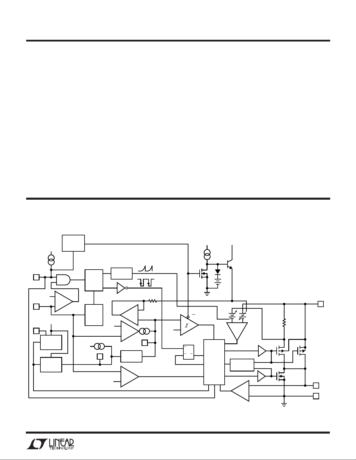
FU CTIO AL DIAGRA
VIN (Pin 6): Main Supply Pin. Must be closely decoupled
to GND, Pin 4.
SYNC/MODE (Pin 7):
This pin performs two functions:
1) synchronize with an external clock and 2) select between two modes of low load current operation. To
synchronize with an external clock, apply a TTL/CMOS
compatible clock with a frequency between 385kHz and
550kHz. To select Burst Mode operation, float the pin or
tie it to VIN. Grounding Pin 7 forces pulse skipping mode
operation.
V
(Pin 8): The Output of a 1.19V ±1% Precision
REF
Reference. May be loaded up to 100µA and is stable with
up to 2000pF load capacitance.
SYNC/MODE
7
V
FB
3
V
REF
8
SHUTDOWN
V
IN
1.5µA
0.6V
V
IN
1.19V
REF
UVLO
TRIP = 2.7V
BURST
DEFEAT
–
+
Y = “0” ONLY WHEN X IS A CONSTANT “1”
Y
X
SLOPE
OSC
FREQ
SHIFT
V
IN
RUN/SS
2.25µA
2
COMP
0.8V
0.86V
+
EA
–
RUN/SOFT
START
+
OVDET
–
V
IN
–
EN
+
0.12V
I
1
TH
–
+
BURST
SLEEP
QRS
SWITCHING
Q
LOGIC
AND
BLANKING
CIRCUIT
V
0.4V
IN
–
+
I
COMP
ANTI-
SHOOT-THRU
I
RCMP
6
V
IN
6Ω
+
–
SW
5
GND
4
1707 BD
5
Page 6

LTC1707
OPERATIO
U
(Refer to Functional Diagram)
Main Control Loop
The LTC1707 uses a constant frequency, current mode
step-down architecture. Both the main (P-channel
MOSFET) and synchronous (N-channel MOSFET) switches
are internal. During normal operation, the internal top
power MOSFET is turned on each cycle when the oscillator
sets the RS latch, and turned off when the current comparator, I
current at which I
the voltage on the ITH pin, which is the output of error
amplifier EA. The VFB pin, described in the Pin Functions
section, allows EA to receive an output feedback voltage
from an external resistive divider. When the load current
increases, it causes a slight decrease in the feedback
voltage relative to the 0.8V reference, which, in turn,
causes the ITH voltage to increase until the average inductor current matches the new load current. While the top
MOSFET is off, the bottom MOSFET is turned on until
either the inductor current starts to reverse as indicated by
the current reversal comparator I
the next cycle.
The main control loop is shut down by pulling the RUN/SS
pin low. Releasing RUN/SS allows an internal 2.25µA
current source to charge soft-start capacitor CSS. When
CSS reaches 0.7V, the main control loop is enabled with the
ITH voltage clamped at approximately 5% of its maximum
value. As CSS continues to charge, ITH is gradually
released, allowing normal operation to resume.
Comparator OVDET guards against transient overshoots
>7.5% by turning the main switch off and keeping it off
until the fault is removed.
Burst Mode Operation
, resets the RS latch. The peak inductor
COMP
resets the RS latch is controlled by
COMP
, or the beginning of
RCMP
When the converter is in Burst Mode operation, the peak
current of the inductor is set to approximately 200mA,
even though the voltage at the ITH pin indicates a lower
value. The voltage at the I
average current is greater than the load requirement. As
the ITH voltage drops below 0.12V, the BURST comparator
trips, causing the internal sleep line to go high and forcing
off both internal power MOSFETs.
In sleep mode, both power MOSFETs are held off and the
internal circuitry is partially turned off, reducing the quiescent current to 200µA. The load current is now being
supplied from the output capacitor. When the output
voltage drops, causing ITH to rise above 0.22V, the top
MOSFET is again turned on and this process repeats.
Short-Circuit Protection
When the output is shorted to ground, the frequency of the
oscillator is reduced to about 35kHz, 1/10 the nominal
frequency. This frequency foldback ensures that the
inductor current has more time to decay, thereby preventing runaway. The oscillator’s frequency will progressively
increase to 350kHz (or the synchronized frequency) when
VFB rises above 0.3V.
Frequency Synchronization
The LTC1707 can be synchronized with an external
TTL/CMOS compatible clock signal with an amplitude of at
least 2V
from 385kHz to 550kHz.
LTC1707 below 385kHz as this may cause abnormal
operation and an undesired frequency spectrum. The top
MOSFET turn-on follows the rising edge of the external
source.
. The frequency range of this signal must be
P-P
pin drops when the inductor’s
TH
Do not
attempt to synchronize the
The LTC1707 is capable of Burst Mode operation in which
the internal power MOSFETs operate intermittently based
on load demand. To enable Burst Mode operation, simply
allow the SYNC/MODE pin to float or connect it to a logic
high. To disable Burst Mode operation and enable pulse
skipping mode, connect the SYNC/MODE pin to GND. In
this mode, efficiency is lower at light loads, but becomes
comparable to Burst Mode operation when the output load
exceeds 30mA.
6
When the LTC1707 is synchronized to an external source,
the LTC1707 operates in PWM pulse skipping mode. In
this mode, when the output load is very low, current
comparator I
and forces the main switch to stay off for the same number
of cycles. Increasing the output load slightly allows constant frequency PWM operation to resume. This mode
exhibits low output ripple as well as low audio noise and
reduced RF interference while providing reasonable low
current efficiency.
remains tripped for more than one cycle
COMP
Page 7

INPUT VOLTAGE (V)
2.5
0
OUTPUT CURRENT (mA)
200
400
600
6.5
1200
1000
1707 F02b
4.5
3.5
7.5
5.5 8.5
800
TJ = 25°C
L = 15µH
EXT SYNC AT 400kHz
V
OUT
= 5V
V
OUT
= 1.5V
V
OUT
= 2.9V
V
OUT
= 3.3V
V
OUT
= 1.8V
V
OUT
= 2.5V
OPERATIO
LTC1707
U
Frequency synchronization is inhibited when the feedback
voltage VFB is below 0.6V. This prevents the external clock
from interfering with the frequency foldback for shortcircuit protection.
Dropout Operation
When the input supply voltage decreases toward the output voltage, the duty cycle increases toward the maximum
on-time. Further reduction of the supply voltage forces the
main switch to remain on for more than one cycle until it
reaches 100% duty cycle. The output voltage will then be
determined by the input voltage minus the voltage drop
across the P-channel MOSFET and the inductor.
In Burst Mode operation or pulse skipping mode operation
with the output lightly loaded, the LTC1707 transitions
through continuous mode as it enters dropout.
Undervoltage Lockout
A precision undervoltage lockout shuts down the LTC1707
when VIN drops below 2.7V, making it ideal for single
lithium-ion battery applications. In lockout, the LTC1707
draws only several microamperes, which is low enough to
prevent deep discharge and possible damage to the lithiumion battery nearing its end of charge. A 100mV hysteresis
ensures reliable operation with noisy input supplies.
Low Supply Operation
The LTC1707 is designed to operate down to a 2.85V input
voltage. At this voltage the converter is most likely to be
running at high duty cycles or in dropout where the main
switch is on continuously. Hence, the I2R loss is due
mainly to the R
of the P-channel MOSFET. See
DS(ON)
Efficiency Considerations in the Applications Information
section.
Below VIN = 4V, the output current must be derated as
shown in Figures 2a and 2b. For applications that require
500mA below VIN = 4V, select the LTC1627.
Figure 2b. Maximum Output Current
vs Input Voltage (Synchronized)
Slope Compensation and Inductor Peak Current
Slope compensation provides stability by preventing subharmonic oscillations. It works by internally adding a ramp
to the inductor current signal at duty cycles in excess of
40%. As a result, the maximum inductor peak current is
lower for V
OUT/VIN
> 0.4 than when V
OUT/VIN
< 0.4. See the
inductor peak current as a function of duty cycle graph in
Figure 3. The worst-case peak current reduction occurs
1200
1000
V
800
600
400
OUTPUT CURRENT (mA)
200
0
2.5
Figure 2a. Maximum Output Current
vs Input Voltage (Unsynchronized)
V
OUT
OUT
V
= 1.8V
= 1.5V
OUT
3.5
= 3.3V
V
OUT
V
= 2.5V
OUT
= 2.9V
4.5
5.5 8.5
INPUT VOLTAGE (V)
1000
50
WITHOUT
EXTERNAL
CLOCK SYNC
70 80
60
90 100
1707 F03
900
V
= 5V
OUT
6.5
TJ = 25°C
L = 15µH
7.5
1707 F02a
800
700
600
MAXIMUM INDUCTOR PEAK CURRENT (mA)
500
0
WORST-CASE
EXTERNAL
CLOCK SYNC
VIN = 4V
10 203040
DUTY CYCLE (%)
Figure 3. Maximum Inductor Peak Current vs Duty Cycle
7
Page 8

LTC1707
WUUU
APPLICATIO S I FOR ATIO
with the oscillator synchronized at its minimum frequency,
i.e., to a clock just above the oscillator free-running
frequency. The actual reduction in average current is less
than for peak current.
The basic LTC1707 application circuit is shown in Figure␣ 1a.
External component selection is driven by the load requirement and begins with the selection of L followed by
CIN and C
Inductor Value Calculation
The inductor selection will depend on the operating frequency of the LTC1707. The internal preset frequency is
350kHz, but can be externally synchronized up to 550kHz.
The operating frequency and inductor selection are interrelated in that higher operating frequencies allow the use
of smaller inductor and capacitor values. However, operating at a higher frequency generally results in lower
efficiency because of increased internal gate charge losses.
The inductor value has a direct effect on ripple current. The
ripple current ∆IL decreases with higher inductance or
frequency and increases with higher VIN or V
Accepting larger values of ∆IL allows the use of low
inductances, but results in higher output voltage ripple
and greater core losses. A reasonable starting point for
setting ripple current is ∆IL = 0.4(I
The inductor value also has an effect on Burst Mode
operation. The transition to low current operation begins
when the inductor current peaks fall to approximately
200mA. Lower inductor values (higher ∆IL) will cause this
to occur at lower load currents, which can cause a dip in
efficiency in the upper range of low current operation. In
Burst Mode operation, lower inductance values will cause
the burst frequency to increase.
Inductor Core Selection
Once the value for L is known, the type of inductor must be
selected. High efficiency converters generally cannot
afford the core loss found in low cost powdered iron cores,
Kool Mµ is a registered trademark of Magnetics, Inc.
OUT.
∆I
1
=
L OUT
fL
()()
.
OUT
V
−
1
V
OUT
V
IN
).
MAX
(1)
forcing the use of more expensive ferrite, molypermalloy,
or Kool Mµ® cores. Actual core loss is independent of core
size for a fixed inductor value, but it is very dependent on
inductance selected. As inductance increases, core losses
go down. Unfortunately, increased inductance requires
more turns of wire and therefore copper losses will
increase.
Ferrite designs have very low core losses and are preferred
at high switching frequencies, so design goals can concentrate on copper loss and preventing saturation. Ferrite
core material saturates “hard,” which means that inductance collapses abruptly when the peak design current is
exceeded. This results in an abrupt increase in inductor
ripple current and consequent output voltage ripple. Do
not allow the core to saturate!
Kool Mµ (from Magnetics, Inc.) is a very good, low loss
core material for toroids with a “soft” saturation characteristic. Molypermalloy is slightly more efficient at high
(>200kHz) switching frequencies but quite a bit more
expensive. Toroids are very space efficient, especially
when you can use several layers of wire, while inductors
wound on bobbins are generally easier to surface mount.
New designs for surface mount are available from
Coiltronics, Coilcraft and Sumida.
CIN and C
In continuous mode, the source current of the top MOSFET
is a square wave of duty cycle V
voltage transients, a low ESR input capacitor sized for the
maximum RMS current must be used. The maximum
RMS capacitor current is given by:
CI
required I
IN MAX
This formula has a maximum at VIN = 2V
I
= I
RMS
monly used for design because even significant deviations
do not offer much relief. Note that capacitor manufacturer’s
ripple current ratings are often based on 2000 hours of life.
This makes it advisable to further derate the capacitor, or
choose a capacitor rated at a higher temperature than
required. Several capacitors may also be paralleled to meet
Selection
OUT
OUT/VIN
VVV
OUT IN OUT
≅
RMS
/2. This simple worst-case condition is com-
OUT
[]
. To prevent large
12/
−
()
V
IN
, where
OUT
8
Page 9

WUUU
APPLICATIO S I FOR ATIO
LTC1707
size or height requirements in the design. Always consult the
manufacturer if there is any question.
The selection of C
is driven by the required effective series
OUT
resistance (ESR). Typically, once the ESR requirement is
satisfied, the capacitance is adequate for filtering. The output
ripple ∆V
∆∆V I ESR
where f = operating frequency, C
is determined by:
OUT
≅+
OUT L
1
fC
4
OUT
= output capacitance
OUT
and ∆IL = ripple current in the inductor. The output ripple
is highest at maximum input voltage since ∆IL increases
with input voltage. For the LTC1707, the general rule for
proper operation is:
C
required ESR < 0.25Ω
OUT
Manufacturers such as Nichicon, United Chemicon and
Sanyo should be considered for high performance throughhole capacitors. The OS-CON semiconductor dielectric
capacitor available from Sanyo has the lowest ESR/size
ratio of any aluminum electrolytic at a somewhat higher
price. Once the ESR requirement for C
has been met,
OUT
the RMS current rating generally far exceeds the
I
RIPPLE(P-P)
requirement. Remember ESR is typically a
direct function of the volume of the capacitor.
In surface mount applications multiple capacitors may
have to be paralleled to meet the ESR or RMS current
handling requirements of the application. Aluminum
electrolytic and dry tantalum capacitors are both available in surface mount configurations. In the case of
tantalum, it is critical that the capacitors are surge tested
for use in switching power supplies. An excellent choice
is the AVX TPS series of surface mount tantalum, available in case heights ranging from 2mm to 4mm. Other
capacitor types include Sanyo POSCAP, KEMET T510
0.8V ≤ V
OUT
≤ 8.5V
and T495 series, Nichicon PL series and Sprague 593D
and 595D series. Consult the manufacturer for other
specific recommendations.
Output Voltage Programming
The output voltage is set by a resistive divider according
to the following formula:
VV
=+
08 1
OUT
.
R
2
R
1
(2)
The external resistive divider is connected to the output,
allowing remote voltage sensing as shown in Figure 4.
Run/Soft-Start Function
The RUN/SS pin is a dual purpose pin that provides the
soft-start function and a means to shut down the LTC1707.
Soft-start reduces surge currents from VIN by gradually
increasing the internal current limit. Power supply
sequencing can also be accomplished using this pin.
An internal 2.25µA current source charges up an external
capacitor CSS. When the voltage on RUN/SS reaches
0.7V the LTC1707 begins operating. As the voltage on
RUN/SS continues to ramp from 0.7V to 1.8V, the internal current limit is also ramped at a proportional linear
rate. The current limit begins at 25mA (at V
and ends at the Figure 3 value (V
RUN/SS
RUN/SS
≈ 1.8V). The
≤ 0.7V)
output current thus ramps up slowly, charging the output
capacitor. If RUN/SS has been pulled all the way to
ground, there will be a delay before the current starts
increasing and is given by:
C
07
t
DELAY
=
SS
A
225..µ
Pulling the RUN/SS pin below 0.4V puts the LTC1707 into
a low quiescent current shutdown (IQ < 15µA). This pin can
be driven directly from logic as shown in Figure 5. Diode
R2
V
FB
LTC1707
GND
Figure 4. Setting the LTC1707 Output Voltage
R1
1707 F04
3.3V OR 5V
RUN/SS
D1
C
SS
Figure 5. RUN/SS Pin Interfacing
RUN/SS
C
SS
1707 F05
9
Page 10

LTC1707
WUUU
APPLICATIO S I FOR ATIO
D1 in Figure 5 reduces the start delay but allows CSS to
ramp up slowly providing the soft-start function. This
diode can be deleted if soft-start is not needed.
Efficiency Considerations
The efficiency of a switching regulator is equal to the
output power divided by the input power times 100%. It is
often useful to analyze individual losses to determine what
is limiting the efficiency and which change would produce
the most improvement. Efficiency can be expressed as:
Efficiency = 100% – (L1 + L2 + L3 + ...)
where L1, L2, etc. are the individual losses as a percentage
of input power.
Although all dissipative elements in the circuit produce
losses, two main sources usually account for most of the
losses in LTC1707 circuits: VIN quiescent current and I2R
losses. The VIN quiescent current loss dominates the
efficiency loss at very low load currents whereas the I2R
loss dominates the efficiency loss at medium to high load
currents. In a typical efficiency plot, the efficiency curve at
very low load currents can be misleading since the actual
power lost is of no consequence as illustrated in Figure 6.
1. The VIN quiescent current is due to two components: the
DC bias current as given in the electrical characteristics
and the internal main switch and synchronous switch
gate charge currents. The gate charge current results
from switching the gate capacitance of the internal power
MOSFET switches. Each time the gate is switched from
high to low or from low to high, a packet of charge dQ
moves from V
current out of V
current. In continuous mode, I
to ground. The resulting dQ/dt is the
IN
that is typically larger than the DC bias
IN
GATECHG
= f(QT + QB) where
QT and QB are the gate charges of the internal top and
bottom switches. Both the DC bias and gate charge losses
are proportional to VIN and thus their effects will be more
pronounced at higher supply voltages.
2. I2R losses are calculated from the resistances of the
internal switches RSW and external inductor RL. In
continuous mode the average output current flowing
through inductor L is “chopped” between the main
switch and the synchronous switch. Thus, the series
resistance looking into SW pin from L is a function of
both top and bottom MOSFET R
and the duty
DS(ON)
cycle (DC) as follows:
RSW = (R
The R
DS(ON)TOP
for both the top and bottom MOSFETs can
DS(ON)
)(DC) + (R
DS(ON)BOT
)(1 – DC)
be obtained from the Typical Performance Characteristics curves. Thus, to obtain I2R losses, simply add R
SW
to RL and multiply by the square of the average output
current.
Other losses including CIN and C
ESR dissipative losses,
OUT
MOSFET switching losses and inductor core and copper
losses generally account for less than 2% total additional
loss.
1
V
= 1.5V
OUT
= 3.3V
V
OUT
= 5V
V
OUT
0.1
0.01
POWER LOST (W)
0.001
1
Figure 6. Power Lost vs Load Current
10 100 1000
LOAD CURRENT (mA)
VIN = 6V
1707 F06
Checking Transient Response
The regulator loop response can be checked by looking at
the load transient response. Switching regulators take
several cycles to respond to a step in load current. When
a load step occurs, V
equal to (∆I
resistance of C
charge C
OUT
• ESR), where ESR is the effective series
LOAD
OUT
, which generates a feedback error signal. The
regulator loop then acts to return V
value. During this recovery time, V
immediately shifts by an amount
OUT
. ∆I
also begins to charge or dis-
LOAD
to its steady-state
OUT
can be monitored
OUT
for overshoot or ringing that would indicate a stability
problem. The internal compensation provides adequate
compensation for most applications. But if additional
compensation is required, the ITH pin can be used for
external compensation as shown in Figure 7 (the 47pF
capacitor, CC2, is typically needed for noise decoupling).
10
Page 11

WUUU
APPLICATIO S I FOR ATIO
LTC1707
A second, more severe transient is caused by switching in
loads with large (>1µF) supply bypass capacitors. The
discharged bypass capacitors are effectively put in parallel
with C
, causing a rapid drop in V
OUT
. No regulator can
OUT
deliver enough current to prevent this problem if the load
switch resistance is low and it is driven quickly. The only
solution is to limit the rise time of the switch drive so that
the load rise time is limited to approximately (25 • C
LOAD
).
Thus, a 10µF capacitor charging to 3.3V would require a
250µs rise time, limiting the charging current to about
130mA.
PC Board Layout Checklist
When laying out the printed circuit board, the following
checklist should be used to ensure proper operation of the
LTC1707. These items are also illustrated graphically in
the layout diagram of Figure 7. Check the following in your
layout:
C
REF
1. Are the signal and power grounds segregated? The
LTC1707 signal ground consists of the resistive
divider, the optional compensation network (RC and
CC1), CSS, C
the (–) plate of CIN, the (–) plate of C
and CC2. The power ground consists of
REF
and Pin 4 of the
OUT
LTC1707. The power ground traces should be kept
short, direct and wide. The signal ground and power
ground should converge to a common node in a starground configuration.
2. Does the VFB pin connect directly to the feedback
resistors? The resistive divider R1/R2 must be connected between the (+) plate of C
and signal ground.
OUT
3. Does the (+) plate of CIN connect to VIN as closely as
possible? This capacitor provides the AC current to the
internal power MOSFETs.
4. Keep the switching node SW away from sensitive small-
signal nodes.
OPTIONAL
C
C2
R
C
C
1
C1
C
SS
BOLD LINES INDICATE HIGH CURRENT PATHS
2
3
4
I
TH
RUN/SS
V
FB
GND
SYNC/MODE
LTC1707
Figure 7. LTC1707 Layout Diagram
8
V
REF
7
6
V
SW
IN
L1
5
+
C
R2
+
C
OUT
R1
IN
V
OUT
–
1707 F07
+
+
V
IN
–
11
Page 12

LTC1707
WUUU
APPLICATIO S I FOR ATIO
Design Example
As a design example, assume the LTC1707 is used in a
single lithium-ion battery-powered cellular phone application. The VIN will be operating from a maximum of 4.2V
down to about 2.85V. The load current requirement is a
maximum of 0.3A but most of the time it will be in standby
mode, requiring only 2mA. Efficiency at both low and high
load currents is important. Output voltage is 2.5V. With
this information we can calculate L using equation (1),
L
1
=
fI
∆
()( )
L
Substituting V
V
OUT
OUT
−
1
= 2.5V, V
V
OUT
V
IN
= 4.2V, ∆IL = 120mA and
IN
(3)
f = 350kHz in equation (3) gives:
V
25
L
350 120
()()
..
kHz mA
−
1
25
42
.
V
=
V
24 1
. µ
H=
A 22µH inductor works well for this application. For best
efficiency choose a 1A inductor with less than 0.25Ω
series resistance.
CIN will require an RMS current rating of at least 0.15A at
temperature and C
will require an ESR of less than
OUT
0.25Ω. In most applications, the requirements for these
capacitors are fairly similar.
For the feedback resistors, choose R1 = 80.6k. R2 can then
be calculated from equation (2) to be:
V
R
2
OUT
08
.
Rk
1 1 171=−
=
; use 169k
Figure 8 shows the complete circuit along with its efficiency curve.
C
ITH
47pF
C
SS
0.1µF
* SUMIDA CD54-220
†
AVX TPSC107M006R0150
††
AVX TPSC226M016R0375
1
2
3
4
8
I
TH
RUN/SS
V
FB
GND
LTC1707
V
REF
SYNC/MODE
V
SW
7
V
6
IN
22µH*
5
R2
169k
1%
+
R1
80.6k
1%
C
OUT
100µF
6.3V
V
2.5V
0.3A
†
OUT
1707 F08a
IN
2.85V TO
4.5V
††
+
C
IN
22µF
16V
100
90
80
70
EFFICIENCY (%)
60
50
Figure 8. Single Lithium-Ion to 2.5V/0.3A Regulator from Design Example
VIN = 3.6V
VIN = 4.2V
V
= 2.5V
OUT
L = 15µH
Burst Mode OPERATION
1 100 1000
10
OUTPUT CURRENT (mA)
1707 F08b
12
Page 13

TYPICAL APPLICATIO S
C
ITH
47pF
C
SS
0.1µF
U
1
2
3
4
5V Input to 3.3V/0.6A Regulator
I
TH
RUN/SS
V
FB
GND
SYNC/MODE
LTC1707
8
V
REF
7
6
V
IN
15µH*
5
SW
* SUMIDA CD54-150
** AVX TPSC107M006R0150
*** TAIYO YUDEN LMK325BJ106K-T
V
OUT
R2
249k
1%
R1
80.6k
1%
3.3V
0.6A
+
C
OUT
100µF
6.3V
C
10µF
**
CERAMIC
1707 TA01
LTC1707
V
= 5V
IN
***
IN
Double Lithium-Ion Battery to 5V/0.5A Low Dropout Regulator
C
ITH
47pF
C
SS
0.1µF
1
2
3
4
I
TH
RUN/SS
V
FB
GND
SYNC/MODE
LTC1707
8
V
REF
7
6
V
IN
5
SW
***
33µH*
* SUMIDA CD54-330
**
AVX TPSD107M010R0100
AVX TPSC226M016R0375
V
OUT
R2
422k
1%
R1
80.6k
1%
5V
0.5A
+
C
OUT
100µF
10V
V
≤ 8.4V
IN
C
***
+
IN
22µF
**
16V
1707 TA02
13
Page 14

LTC1707
TYPICAL APPLICATIO S
C
ITH
47pF
C
SS
0.1µF
* SUMIDA CD54-100
** TAIYO YUDEN LMK325BJ106K-T
†
AVX TPSC107M006R0150
U
3.3V Input to 2.5V/0.4A Regulator
1
2
3
4
I
TH
RUN/SS
V
FB
GND
SYNC/MODE
LTC1707
8
V
REF
7
6
V
IN
SW
10µH*
5
169k
1%
80.6k
1%
V
= 3.3V
IN
V
OUT
2.5V
R2
R1
0.4A
†
C
+
C
OUT
100µF
6.3V
IN
10µF
CERAMIC
1707 TA03
**
C
ITH
47pF
C
SS
0.1µF
Double Lithium-Ion to 2.5V/0.5A Regulator
1
2
3
4
I
TH
RUN/SS
V
FB
GND
SYNC/MODE
LTC1707
8
V
REF
7
6
V
IN
5
SW
* SUMIDA CD54-250
** AVX TPSC107M006R0150
*** AVX TPSC226M016R0375
25µH*
R2
169k
+
1%
R1
80.6k
1%
V
2.5V
0.5A
C
OUT
100µF
6.3V
OUT
V
≤ 8.4V
IN
***
C
+
IN
22µF
**
16V
1707 TA05
14
Page 15

PACKAGE DESCRIPTIO
U
Dimensions in inches (millimeters) unless otherwise noted.
S8 Package
8-Lead Plastic Small Outline (Narrow 0.150)
(LTC DWG # 05-08-1610)
0.189 – 0.197*
(4.801 – 5.004)
7
8
5
6
LTC1707
0.228 – 0.244
(5.791 – 6.197)
0.010 – 0.020
(0.254 – 0.508)
0.008 – 0.010
(0.203 – 0.254)
*
DIMENSION DOES NOT INCLUDE MOLD FLASH. MOLD FLASH
SHALL NOT EXCEED 0.006" (0.152mm) PER SIDE
**
DIMENSION DOES NOT INCLUDE INTERLEAD FLASH. INTERLEAD
FLASH SHALL NOT EXCEED 0.010" (0.254mm) PER SIDE
×
°
45
0.016 – 0.050
(0.406 – 1.270)
(1.346 – 1.752)
0°– 8° TYP
0.053 – 0.069
0.014 – 0.019
(0.355 – 0.483)
TYP
0.150 – 0.157**
(3.810 – 3.988)
1
3
2
4
0.004 – 0.010
(0.101 – 0.254)
0.050
(1.270)
BSC
SO8 1298
15
Page 16

LTC1707
TYPICAL APPLICATIO
C
ITH
47pF
C
SS
0.1µF
U
Single Lithium-Ion to 1.8V/0.3A Regulator
1
2
3
4
I
TH
RUN/SS
V
FB
GND
SYNC/MODE
LTC1707
8
V
REF
7
6
V
IN
5
SW
* SUMIDA CD54-150
** AVX TPSC107M006R0150
*** TAIYO YUDEN LMK325BJ106K-T
15µH*
R2
100k
+
1%
R1
80.6k
1%
V
1.8V
0.3A
C
OUT
100µF
6.3V
OUT
V
≤ 4.2V
IN
CIN***
10µF
**
CERAMIC
1707 TA04
RELATED PARTS
PART NUMBER DESCRIPTION COMMENTS
LTC1174/LTC1174-3.3 High Efficiency Step-Down and Inverting DC/DC Converters Monolithic Switching Regulators, I
LTC1174-5 Burst Mode Operation
LTC1265 1.2A, High Efficiency Step-Down DC/DC Converter Constant Off-Time, Monolithic, Burst Mode Operation
LT®1375/LT1376 1.5A, 500kHz Step-Down Switching Regulators High Frequency, Small Inductor, High Efficiency
LTC1436A/LTC1436A-PLL High Efficiency, Low Noise, Synchronous Step-Down Converters 24-Pin Narrow SSOP
LTC1438/LTC1439 Dual, Low Noise, Synchronous Step-Down Converters Multiple Output Capability
LTC1474/LTC1475 Low Quiescent Current Step-Down DC/DC Converters Monolithic, I
LTC1504A Monolithic Synchronous Step-Down Switching Regulator Low Cost, Voltage Mode I
from 4V to 10V
V
IN
to 250mA, IQ = 10µA, 8-Pin MSOP
OUT
OUT
LTC1626 Low Voltage, High Efficiency Step-Down DC/DC Converter Monolithic, Constant Off-Time, I
Low Supply Voltage Range: 2.5V to 6V
LTC1627 Monolithic Synchronous Step-Down Switching Regulator Constant Frequency, I
Regulation, V
from 2.65V to 8.5V
IN
to 500mA, Secondary Winding
OUT
LTC1622 Low Input Voltage Current Mode Step-Down DC/DC Controller 550kHz Constant Frequency, External P-Channel Switch,
to 4A, VIN From 2V to 10V
I
OUT
LTC1735 High Efficiency, Synchronous Step-Down Converter 16-Pin SO and SSOP
to 450mA,
OUT
to 500mA,
to 600mA,
OUT
16
Linear Technology Corporation
1630 McCarthy Blvd., Milpitas, CA 95035-7417
(408) 432-1900 ● FAX: (408) 434-0507
●
www.linear-tech.com
1707i LT/TP 1299 4K • PRINTED IN USA
LINEAR TECHNOLOGY CORPORATION 1999
 Loading...