

Page 1
LTC1706-82
Final Electrical Specifications
VID Voltage Programmer
for Intel VRM 9.0
FEATURES
■
Fully Compliant with the Intel VRM 9.0 VID
Specification
■
Programs Regulator Output Voltage from 1.10V to
1.85V in 25mV Steps
■
Programs an Entire Family of Linear Technology
DC/DC Converters
■
±0.25% Accurate Voltage Divider
■
Built-In 40k Pull-Up Resistors on Program Inputs
■
Available in MSOP-10 Packaging
U
APPLICATIO S
■
Intel Pentium® III Processor Power Supply
■
Multiprocessor Workstations and Servers
■
Multiphase Processor Power Supply
■
AMD AthlonTM Processor Power Supply
U
January 2000
DESCRIPTIO
The LTC®1706-82 is a precision, digitally programmed,
resistive ladder which adjusts the output of any 0.8V
referenced regulator. Depending on the state of the five
VID inputs, an output voltage between 1.10V and 1.85V is
programmed in 25mV increments.
The LTC1706-82 is designed specifically to program an
entire family of Linear Technology DC/DC converters in full
compliance with the Intel Desktop VID specification.
The LTC1706-82 programs the following Linear Technology DC/DC converter products: LTC1622, LTC1628,
LTC1629, LTC1702, LTC1735, LTC1735-1, LTC1772 and
LTC1929.
Consult factory for future compatible DC/DC converter
products.
, LTC and LT are registered trademarks of Linear Technology Corporation.
Pentium is a registered trademark of Intel Corporation.
AMD Athlon is a trademark of Advanced Micro Devices, Inc.
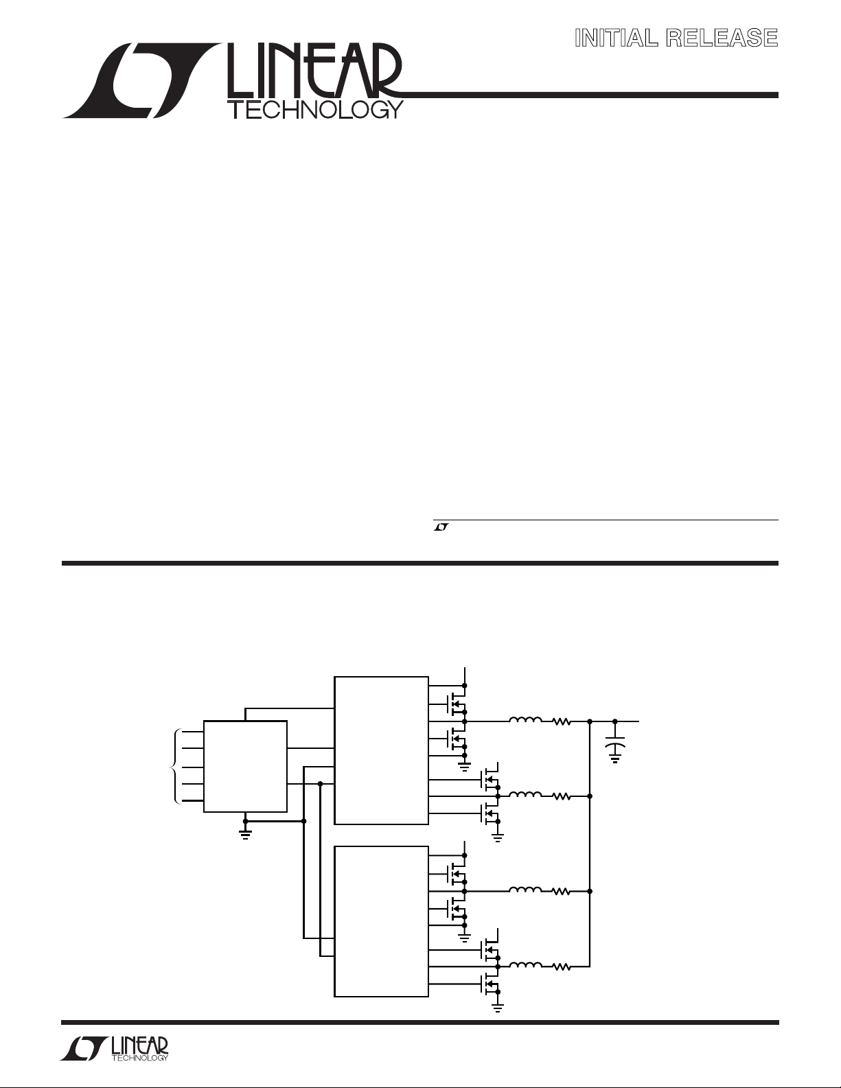
TYPICAL APPLICATIO
VID Controlled High Current 4-Phase DC/DC Converter (Simplified Block Diagram)
V
CC
VID0
FROM
µP
VID1
VID2
LTC1706-82
VID3
VID4
GND
UP TO SIX LTC1629s CAN BE PARALLELED
TO DELIVER AS MUCH AS 200A
SENSE
U
V
IN
4.5V TO 22V
V
IN
INTV
CC
LTC1629
V
DIFFOUT
SGND
FB
EAIN
LTC1629
SGND
EAIN
TG1
SW1
BG1
PGND
TG2
SW2
BG2
V
TG1
SW1
BG1
PGND
TG2
SW2
BG2
IN
V
IN
4.5V TO 22V
L1 R
SENSE1
V
IN
R
L2
SENSE2
R
L3
SENSE3
V
IN
R
L4
SENSE4
1706-82 TA01
+
V
OUT
1.10V TO 1.85V
UP TO 70A
C
OUT
Information furnished by Linear Technology Corporation is believed to be accurate and reliable.
However, no responsibility is assumed for its use. Linear Technology Corporation makes no representation that the interconnection of its circuits as described herein will not infringe on existing patent rights.
1
Page 2
LTC1706-82
WW
W
ABSOLUTE AXI U RATI GS
U
UUW
PACKAGE/ORDER I FOR ATIO
(Note 1)
(Voltages Referred to GND Pin)
Input Supply Voltage (VCC) ..........................–0.3V to 7V
VID Input Pins .............................................– 0.3V to 7V
SENSE Pin ...................................................–0.3V to 7V
FB Pin ..........................................................–0.3V to 7V
Operating Temperature Range (Note 2) .. – 40°C to 85°C
TOP VIEW
1
VID0
2
VID1
3
VID2
4
VID3
5
V
CC
MS10 PACKAGE
10-LEAD PLASTIC MSOP
10
FB
9
GND
8
NC
7
VID4
6
SENSE
ORDER PART
NUMBER
LTC1706EMS-82
MS10
PART MARKING
Junction Temperature........................................... 110°C
Storage Temperature Range ................. –65°C to 150°C
T
= 110°C, θJA = 120°C/W
JMAX
LTMJ
Lead Temperature (Soldering, 10 sec).................. 300°C
Consult factory for Industrial and Military grade parts.
ELECTRICAL CHARACTERISTICS
The ● denotes the specifications which apply over the full operating temperature range, otherwise specifications are at TA = 25°C.
2.7V ≤ VCC ≤ 5.5V, VIDO = VID1 = VID2 = VID3 = VID4 = NC unless otherwise specified.
SYMBOL PARAMETER CONDITIONS MIN TYP MAX UNITS
V
CC
I
VCC
R
FB-SENSE
V
Error % Output Voltage Accuracy Programmed From 1.10V to 1.85V ● –0.25 0.25 %
OUT
R
PULLUP
VID
T
I
VID-LEAK
V
PULLUP
Note 1: Absolute Maximum Ratings are those values beyond which the life
of a device may be impaired.
Note 2: The LTC1706-82 is guaranteed to meet performance specifications
from 0°C to 70°C. Specifications over the –40°C to 85°C operating
temperature range are assured by design, characterization and correlation
with statistical process controls.
Operating Supply Voltage Range 2.7 5.5 V
Supply Current (Note 3) 0.1 5.0 µA
Resistance Between SENSE and FB ● 61014 kΩ
VID Input Pull-Up Resistance V
VID Input Voltage Threshold V
VID Input Leakage Current VCC < VID < 7V, (Note 4) 0.01 ±1.00 µA
VID Pull-Up Voltage VCC = 3.3V 2.8 V
= 0.6V, (Note 4) 40 kΩ
DIODE
(2.7V < VCC < 5.5V) 0.4 V
IL
V
(2.7V < VCC < 5.5V) 1.6 V
IH
V
= 5V 4.5 V
CC
Note 3: With all five VID inputs floating, the VCC supply current is simply
the device leakage current. However, the V
be approximately equal to the number of grounded VID input pins times
(VCC – 0.6V)/40k. (See the Applications Information section for more
detail.)
Note 4: Each built-in pull-up resistor attached to the VID inputs also has a
series diode connected to V
supply without damage or clamping. (See Operation section for further
details.)
to allow input voltages higher than the V
CC
supply current will rise and
CC
CC
2
Page 3
UW
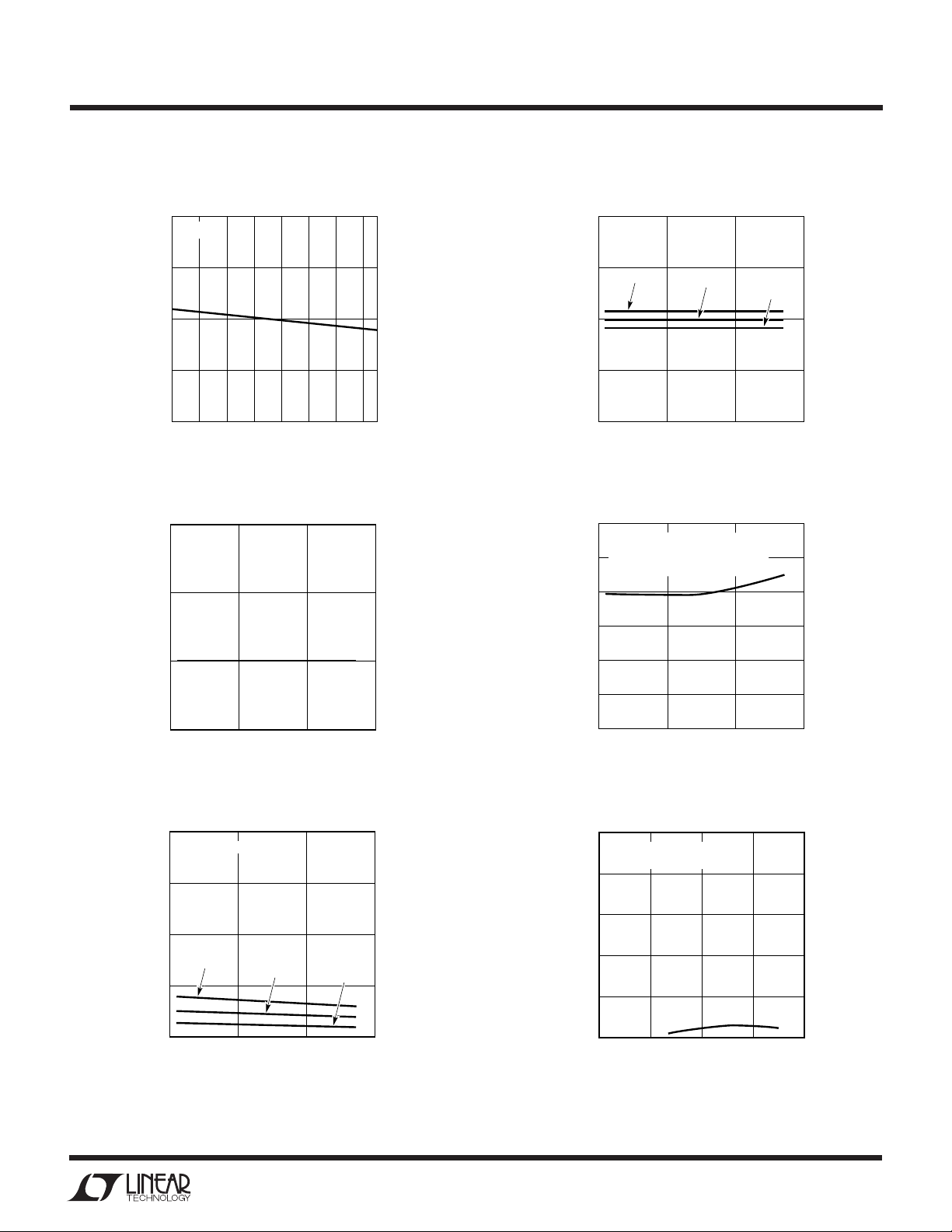
TEMPERATURE (°C)
–50 0 50 100
ERROR (%)
1706-82 G02
0.25
0
–0.25
V
OUT
= 1.85V
V
OUT
= 1.5V
V
OUT
= 1.1V
TEMPERATURE (°C)
–50 0 50 100
VID PULL-UP CURRENT (µA)
1706-82 G04
120
100
80
60
40
20
0
VCC = 5V
VID4 = 0V
VID0 = VID1 = VID2 = VID3 = OPEN
SUPPLY VOLTAGE (V)
02468
SUPPLY CURRENT (µA)
1706-82 G06
5
4
3
2
1
0
ALL VID INPUTS OPEN
T
A
= 25°C
TYPICAL PERFOR A CE CHARACTERISTICS
Typical Error % vs Output Voltage Typical Error % vs Temperature
0.25
TA = 25°C
0
ERROR (%)
LTC1706-82
(kΩ)
R
FB1
–0.25
1.2 1.3 1.4 1.5 1.6 1.7 1.8
1.1
R
FB1
30
20
10
0
–50 0 50 100
OUTPUT VOLTAGE (V)
1706-82 G01
vs Temperature I
TEMPERATURE (°C)
1706-82 G03
VID-PULLUP
vs Temperature
Supply Current vs Temperature Supply Current vs Supply Voltage
2.0
ALL VID INPUTS OPEN
1.5
1.0
SUPPLY CURRENT (µA)
VCC = 5V
0.5
0
–50 0 50 100
VCC = 3.3V
TEMPERATURE (°C)
VCC = 2.7V
1706-82 G05
3
Page 4

LTC1706-82
UUU
PI FU CTIO S
VID0 (Pin 1): LSB Programming Input. Low = GND,
High = V
or Float. Grounding VID0 adds 25mV to the
CC
output sense voltage.
VID1 (Pin 2): 4th MSB Programming Input. Low = GND,
High = VCC or Float. Grounding VID1 adds 50mV to the
output sense voltage.
VID2 (Pin 3): 3rd MSB Programming Input. Low = GND,
High = VCC or Float. Grounding VID2 adds 100mV to the
output sense voltage.
SENSE (Pin 6): Regulator Output Voltage. Connect directly to regulator output sense node or V
DIFFOUT
used with the LTC1629 and LTC1929.
VID4 (Pin 7): MSB Programming Input. Low = GND,
High = VCC or Float. Grounding VID4 adds 400mV to the
output sense voltage.
NC (PIN 8): No Connect.
GND (Pin 9): Ground. Connect to regulator signal ground.
FB (Pin 10): Feedback Input. Connect to the 0.8V feedback
VID3 (Pin 4): 2nd MSB Programming Input. Low = GND,
High = VCC or Float. Grounding VID3 adds 200mV to the
output sense voltage.
pin of a compatible regulator or the EAIN pin of the
LTC1629 and LTC1929.
VCC (Pin 5): Power Supply Voltage. Range from 2.7V to
5.5V.
PIUTABLE
NOMINAL (V) ABSOLUTE MAX (V)
PIN NAME DESCRIPTION MIN TYP MAX MIN MAX
1 VID0 LSB Programmable Input 0 V
2 VID1 3rd MSB Programmable Input 0 V
3 VID2 2nd MSB Programmable Input 0 V
4 VID3 1st MSB Programmable Input 0 V
5V
6 SENSE Regulator Output Voltage 1.075 1.85 –0.3 7
7 VID4 MSB Programmable Input 0 V
8NC
9 GND Ground 0 –0.3 7
10 FB 0.8V Feedback Input 0 0.8 1.5 –0.3 7
CC
Power Supply 2.7 5.5 –0.3 7
CC
CC
CC
CC
CC
–0.3 7
–0.3 7
–0.3 7
–0.3 7
–0.3 7
when
4
Page 5

BLOCK DIAGRA
V
CC
40k
VID0
1
V
CC
40k
VID1
2
V
CC
40k
VID2
3
V
CC
W
LTC1706-82
V
CC
5
6
SENSE
R
FB1
10k
10
FB
SWITCH
CONTROL
LOGIC
V
CC
R
FB2
9
GND
1706-82 BD
VID3
40k
4
VID4
7
40k
U
OPERATIO
The LTC1706-82 is a precision resistive divider designed
specifically for use with an entire family of Linear Technology Corporation DC/DC switching regulators with 0.8V
internal reference and feedback voltages. The LTC1706-82
produces an output voltage ranging from 1.10V to 1.85V
in 25mV steps by closing the loop between the output
voltage sense and the feedback input of the regulator with
the appropriate resistive divider network.
The “top” feedback resistor, R
SENSE and FB, is typically 10k and is not modified by the
state of the VID program inputs.
The “bottom” feedback resistor, R
fied by the five VID inputs and is precisely ratioed to R
, connected between
FB1
, however is modi-
FB2
FB1
.
VID Programming
A list of programmed inputs and their corresponding
output voltages is shown in Table 1. Programming is
accomplished by applying the proper voltage (or float
condition) on the five digital VID inputs. VID4 is the most
significant bit (MSB) and VID0 is the least significant bit
(LSB).
When the five VID inputs are low, or grounded, the
regulator output voltage is set to 1.85V. Each increasing
binary count is equivalent to a decrease of 25mV in the
output voltage. Therefore, to obtain a 1.10V output, only
VID0 is grounded while the other four VID inputs are tied
high or floating.
When all five VID inputs are high or floating, such as when
no CPU is present in a system, a regulated 1.075V output
is generated at V
SENSE
.
5
Page 6

LTC1706-82
U
OPERATIO
Each VID input pin is pulled up by a 40k resistor in series
with a diode connected to VCC. Therefore, it should be
grounded (or driven low) to produce a digital low input. It
can be either floated or connected to VCC to get a digital
high input. The series diode is included to prevent the input
from being damaged or clamped when it is driven higher
than VCC.
Voltage Sensing and Feedback Pins
The FB pin is a high impedance node that requires minimum layout distance to reduce extra loading and unwanted stray pickup.
When used with the LTC1629, the LTC1706-82’s FB,
SENSE, VCC and GND pins should be connected, respectively, with the EAIN, V
DIFFOUT
, INTVCC, and SGND pins of
the LTC1629. The result of this application is a precisely
controlled, multiphase, variable output voltage supply to
any low voltage, high current system such as a powerful
personal computer, workstation or network server. True
remote sense capability of the LTC1629 is also retained in
this case.
VID Input Characteristics
The VID inputs should be driven with a maximum VIL of
0.4V and a minimum VIH of 1.6V. However, the VID input
range is not limited to values less than VCC. Because of the
internal diode between VCC and the pull-up resistor, the
inputs can go higher than VCC without being clamped to
VCC or damaging the input.
This allows the LTC1706-82 to be fully logic compatible
and operational over a higher input voltage range (less
than the 7V absolute maximum rating).
When a VID input is grounded, there will be a higher
quiescent current flow from Vcc because of a resistor from
Vcc through a series diode to each one of the VID inputs.
This increase in quiescent current is calculated from
Table 1. VID Inputs and Corresponding Output Voltage
CODE VID4 VID3 VID2 VID1 VID0 OUTPUT
00000 GND GND GND GND GND 1.850
00001 GND GND GND GND Float 1.825
00010 GND GND GND Float GND 1.800
00011 GND GND GND Float Float 1.775V
00100 GND GND Float GND GND 1.750V
00101 GND GND Float GND Float 1.725V
00110 GND GND Float Float GND 1.700V
00111 GND GND Float Float Float 1.675V
01000 GND Float GND GND GND 1.650V
01001 GND Float GND GND Float 1.625V
01010 GND Float GND Float GND 1.600V
01011 GND Float GND Float Float 1.575V
01100 GND Float Float GND GND 1.550V
01101 GND Float Float GND Float 1.525V
01110 GND Float Float Float GND 1.500V
01111 GND Float Float Float Float 1.475V
10000 Float GND GND GND GND 1.450V
10001 Float GND GND GND Float 1.425V
10010 Float GND GND Float GND 1.400V
10011 Float GND GND Float Float 1.375V
10100 Float GND Float GND GND 1.350V
10101 Float GND Float GND Float 1.325V
10110 Float GND Float Float GND 1.300V
10111 Float GND Float Float Float 1.275V
11000 Float Float GND GND GND 1.250V
11001 Float Float GND GND Float 1.250V
11010 Float Float GND Float GND 1.200V
11011 Float Float GND Float Float 1.175V
11100 Float Float Float GND GND 1.150V
11101 Float Float Float GND Float 1.125V
11110 Float Float Float Float GND 1.100V
11111 Float Float Float Float Float NO_CPU
(1.075V)
IQ = N(VCC – V
N is the number of grounded VID inputs. V
0.6V while R
PULLUP
)/R
DIODE
PULLUP
DIODE
is typically
has a typical pullup resistance of 40k.
In other words, each VID input has a typical pull up current
of (VCC – 0.6)/40K, which is approximately 68µA for a 3.3V
system.
6
Page 7

LTC1706-82
U
WUU
APPLICATIO S I FOR ATIO
Besides the LTC1629, the LTC1706-82 also programs a
whole family of LTC DC/DC converters that have an onboard
0.8V reference. The LTC1628, LTC1735, LTC1622,
LTC1702, LTC1772 and LTC1929 are just a few of the high
efficiency step-down switching regulators that will work
equally well with the LTC1706-82.
U
PACKAGE DESCRIPTIO
0.007
(0.18)
0.021
± 0.006
(0.53 ± 0.015)
* DIMENSION DOES NOT INCLUDE MOLD FLASH, PROTRUSIONS OR GATE BURRS. MOLD FLASH,
PROTRUSIONS OR GATE BURRS SHALL NOT EXCEED 0.006" (0.152mm) PER SIDE
** DIMENSION DOES NOT INCLUDE INTERLEAD FLASH OR PROTRUSIONS.
INTERLEAD FLASH OR PROTRUSIONS SHALL NOT EXCEED 0.006" (0.152mm) PER SIDE
° – 6° TYP
0
Dimensions in inches (millimeters) unless otherwise noted.
MS10 Package
10-Lead Plastic MSOP
(LTC DWG # 05-08-1661)
0.040
± 0.006
(1.02 ± 0.15)
SEATING
PLANE
0.009
(0.228)
0.0197
REF
(0.50)
BSC
0.034 ± 0.004
(0.86 ± 0.102)
0.006 ± 0.004
(0.15 ± 0.102)
0.118 ± 0.004*
(3.00 ± 0.102)
0.193 ± 0.006
(4.90 ± 0.15)
12
8910
3
7
6
45
0.118 ± 0.004**
(3.00 ± 0.102)
MSOP (MS10) 1098
7
Page 8

LTC1706-82
TYPICAL APPLICATIO
OPTIONAL SYNC
CLOCK IN
5
V
VID0
VID1
VID2
VID3
VID4
CC
SENSE
LTC1706-82
GND
9
6
10
FB
FROM
1
2
3
µP
4
7
U
VID Controlled High Current 70A 4-Phase Power Supply
0.33µF
47k
24k
0.33µF
100pF
75k
1000pF
6800pF
1000pF
10
11
12
13
14
1
2
3
4
5
6
7
8
9
RUN/SS
SENSE1
SENSE1
EAIN
PLLFLTR
PLLIN
PHASMD
I
TH
SGND
V
DIFFOUT
–
V
OS
+
V
OS
SENSE2
SENSE2
+
–
LTC1629
–
+
CLKOUT
TG1
SW1
BOOST1
BG1
EXTV
INTV
PGND
BG2
BOOST2
SW2
TG2
AMPMD
28
5V
27
26
25
24
V
IN
23
22
CC
21
CC
20
19
18
17
16
15
0.47µF
D7
D8
0.47µF
1µF
1µF
25V
10Ω
+
22µF
6.3V
M1
150µF, 16V
× 2
+
M4
GND
L1
0.003Ω
D1
MBRS
M3
M6
340T3
× 3
470µF, 6.3V
KEMET CAP
D2
MBRS
340T3
0.003Ω
+
V
OUT
1.10V TO
1.85V
70A
M2
M5
L2
GND
M8
M11
L3
0.003Ω
D3
MBRS
340T3
M9
× 3
470µF, 6.3V
KEMET CAP
+
V
IN
12V
D4
MBRS
M12
340T3
0.003Ω
L4
1706-82 TA02
: 12V
V
IN
V
: 1.1V TO 1.85, 70A
OUT
M1 TO M12: FDS7760A
L1 TO L4: 1µH SUMIDA CEPH149-IROMC
D7 TO D10: CENTROL CMDSH-3TR
: KEMET T510X477M006AS
C
OUT
47pF
0.01µF
10k
100pF
1nF
1000pF
NC
1000pF
10
11
12
13
14
1
2
3
4
5
6
7
8
9
RUN/SS
SENSE1
SENSE1
EAIN
PLLFLTR
PLLIN
PHASMD
I
TH
SGND
V
DIFFOUT
–
V
OS
+
V
OS
SENSE2
SENSE2
+
–
LTC1629
–
+
CLKOUT
TG1
SW1
BOOST1
BG1
EXTV
INTV
PGND
BG2
BOOST2
SW2
TG2
AMPMD
28
5V
27
26
25
24
V
IN
23
22
CC
21
CC
20
19
18
17
16
15
0.47µF
D9
D10
0.47µF
1µF
1µF
25V
22µF
6.3V
M7
150µF, 16V
× 2
+
M10
10Ω
+
RELATED PARTS
PART NUMBER DESCRIPTION COMMENTS
LTC1622 Sychnronizable Low Voltage Step-Down Controller 8-Pin MSOP, 2V ≤ VIN ≤ 10V, 550kHz, Burst ModeTM Operation
LTC1628 Dual High Efficiency, 2-Phase Synchronous Step-Down Controller Constant, Standby, 5V and 3.3V LDOs, 3.5V ≤ VIN ≤ 36V
LTC1629 PolyPhaseTM High Efficiency Step-Down DC/DC Controller Expandable Up to 12 Phases, Up to 120A, Remote Sense Diff Amp
LTC1702/LTC1703 Dual High Efficiency, 2-Phase Synchronous Step-Down Controller 550kHz, 25MHz GBW, No R
LTC1706-81 VID Voltage Programmer with Desktop Code VRM 8.2-VRM 8.4, V
OUT
LTC1709 2-Phase Synchronous Step-Down Controller with 5-Bit Desktop VID 4V ≤ VIN ≤ 36V, PLL, 36-Pin SSOP, Current Mode Operation
LTC1735 High Efficiency Synchronous Step-Down Controller Burst Mode Operation, 16-Pin Narrow SSOP, Fault Protection,
3.5V ≤ V
≤ 36V
IN
LTC1736 High Efficiency Synchronous Buck Controller with 5-Bit Mobile VID GN-24, Power Good, Output Fault Protection, 3.5V ≤ VIN ≤ 36V
LTC1772 SOT-23 Low Voltage Step-Down Controller 6-Pin SOT-23, 2.5V ≤ VIN ≤ 10V, 550kHz, Burst Mode Operation
LTC1929 2-Phase Synchronous Step-Down Controller Current Mode Operation, I
Burst Mode, PolyPhase and No R
are trademarks of Linear Technology Corporation.
SENSE
Linear Technology Corporation
8
1630 McCarthy Blvd., Milpitas, CA 95035-7417
(408) 432-1900 ● FAX: (408) 434-0507
●
www.linear-tech.com
TM
, 2.7V ≤ VIN ≤ 7V
SENSE
Range: 1.3V to 3.5V
Up to 40A, 3.5V ≤ VIN ≤ 36V
OUT
170682i LT/TP 0100 4K • PRINTED IN USA
LINEAR TECHNOLOGY CORPORATION 2000
 Loading...