

Page 1
FEATURES
■
Complete SMBus/I2CTM Brushless DC Fan Speed
Control System in a 5-Pin SOT-23 package
■
0.75Ω PMOS Linear Regulator with 180mA
Output Current Rating
■
0V to 4.922V Output Voltage Range Controlled by a
6-Bit DAC
■
Simple 2-Wire SMBus/I2C Interface
■
250ms Internal Timer Ensures Fan Start-Up
■
Current Limit and Thermal Shutdown
■
Fault Status Indication via SMBus Host Readback
U
APPLICATIO S
■
Notebook Computers
■
Spot Cooling
■
Portable Instruments
■
Battery-Powered Systems
■
DC Motor Control
■
White LED Power Supplies
■
Programmable Low Dropout Regulator
, LTC and LT are registered trademarks of Linear Technology Corporation.
2
C is a trademark of Philips Electronics N.V.
I
LTC1695
SMBus/I2C Fan Speed
Controller in SOT-23
U
DESCRIPTIO
The LTC®1695 fan speed controller provides all the functions necessary for a power management microprocessor
to regulate the speed of a 5V brushless DC fan via a 2-wire
SMBus/I2C interface. Fan speed is controlled according to
the system’s required temperature profile and permits
lower fan power consumption, longer battery run time and
lower acoustical generated noise versus systems that
only provide simple on-off control for the fan.
The LTC1695 incorporates a 180mA low dropout linear
regulator, a 2-wire SMBus/I2C interface and a 6-bit DAC.
Fan speed is controlled by varying the fan’s terminal
voltage through the output voltage of the LTC1695’s linear
regulator. The LTC1695’s output voltage is programmed
by sending a 6-bit digital code to the LTC1695 DAC via the
SMBus. To eliminate fan start-up problems at lower fan
voltages, users can enable the LTC1695’s boost start
feature that provides the DAC’s full-scale output voltage
for 250ms before decreasing to the programmed output
voltage.
The LTC1695 includes output current limiting and thermal
shutdown as well as status monitors that can be read back
by the microprocessor during fault conditions. The
LTC1695 is available in a 5-lead SOT-23 package.
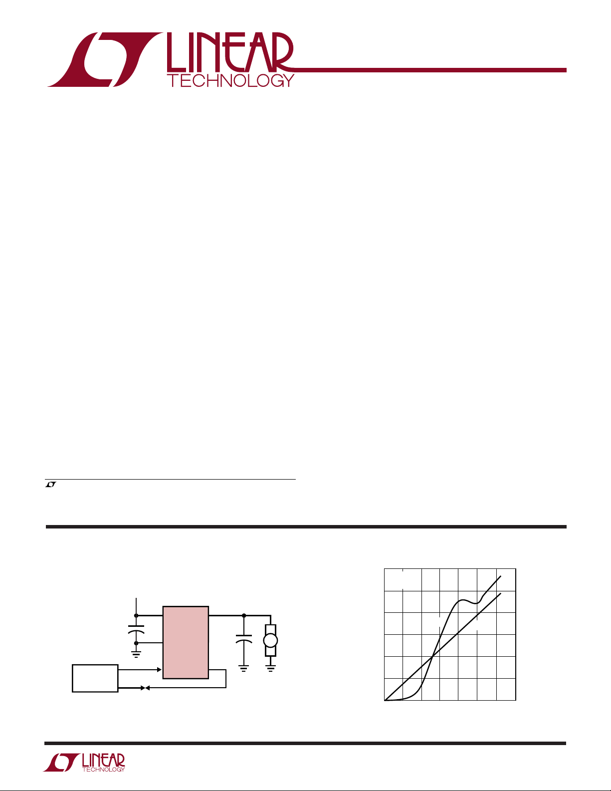
TYPICAL APPLICATION
5V
15
V
V
CC
+
10µF
2
3
SYSTEM
CONTROLLER
LTC1695
GND
SCL
OUT
SDA
U
4
4.7µF
Fan Voltage and Current vs DAC Code
120
VCC = 5V
= 25°C
T
A
100
80
+
5V DC FAN
SUNON
KDE0502PFB2-8
0.6W, 1.7 CFM
(25 • 25 • 10)mm
1695 • TA01
60
3
40
LOAD CURRENT (mA)
20
0
0
10 20
I
LOAD
40 60 70
30 50
DAC CODE
V
OUT
6
5
OUTPUT VOLTAGE (V)
4
3
2
1
0
1695 • TA02
1
Page 2
LTC1695
WW
W
ABSOLUTE AXI U RATI GS
U
UUW
PACKAGE/ORDER I FOR ATIO
(Note 1)
Terminal Voltages
Supply Voltage (VCC) ............................................. 7V
All Other Inputs ........................ –0.3V to (V
+ 0.3V)
CC
Operating Temperature Range ..................... 0°C to 70°C
GND 2
SCL 3
Junction Temperature........................................... 125°C
Storage Temperature Range ..................–65°C to 150°C
Lead Temperature (Soldering, 10 sec)..................300°C
Consult factory for Industrial and Military grade parts.
ELECTRICAL CHARACTERISTICS
temperature range, otherwise specifications are at TA = 25°C. V
SYMBOL PARAMETER CONDITIONS MIN TYP MAX UNITS
V
CC
I
CC
DAC
V
LSB
V
OS
DNL Differential Nonlinearity I
INL Integral Nonlinearity I
V
FS
V
ZS
R
ON(P)
Timer and Thermal Shutdown
V
UVLO
T
BST_ST
T
THERMAL
I
FAULT
SMBus SCL, SDA Inputs
V
IH
V
IL
I
IN
C
IN
t
ON
t
OFF
V
OL
Supply Voltage Range 4.5 5 5.5 V
Supply Current, Operating V
Supply Current, Shutdown DAC Code = 0
DAC Resolution Guaranteed Monotonic ● 6 Bits
1LSB Resolution I
Offset Error I
V
, DAC Full Scale I
OUT
V
, DAC Zero Scale R
OUT
P-Channel On Resistance I
Undervoltage Lockout Voltage Rising V
Boost Start Timer I
Thermal Shutdown Temperature (Note 3) 155 °C
Output Current Limit Threshold V
Input High Threshold ● 2.1 V
Input Low Threshold ● 0.8 V
Input Current SCL, SDA = 0V or 5V ● ±0.1 ±5 µA
Input Capacitance (Note 3) 3 pF
Switch On Time from V
Stop Condition (f
Switch Off Time from V
Stop Condition (f
SDA Output Low Voltage I
= 100kHz) I
SMBus
= 100kHz) I
SMBus
The ● denotes the specifications which apply over the full operating
= 5V unless otherwise stated.
CC
= Full Scale, I
OUT
= 1mA ● 73 78 83 mV
LOAD
= 1mA ● ±1 LSB
LOAD
= 1mA (Note 2) ● ±0.75 LSB
LOAD
= 1mA (Note 2) ● ±0.75 LSB
LOAD
= 20mA ● 4.5 4.93 V
LOAD
= 150mA ● 4.5 4.9 V
I
LOAD
= 1kΩ ● 085 mV
LOAD
= 150mA 0.75 Ω
LOAD
CC
= 10mA, C
LOAD
= 0V, DAC Code = 63 ● 180 390 850 mA
OUT
from Zero Scale to Full Scale, ● 50 500 µs
OUT
= 1mA, C
LOAD
from Full Scale to Zero Scale, ● 150 500 µs
OUT
= 150mA, C
LOAD
= 3mA ● 150 400 mV
PULLUP
LOAD
= 4.7µF ● 75 250 1000 ms
LOAD
= 4.7µF
LOAD
LOAD
TOP VIEW
V
1
CC
S5 PACKAGE
5-LEAD PLASTIC SOT-23
T
= 125°C, θJA = 256°C/W
JMAX
SEE THE APPLICATIONS
INFORMATION SECTION.
= 150mA ● 150.7 155 mA
= 4.7µF
5 V
OUT
4 SDA
● 80 200 µA
● 2.3 2.9 3.5 V
ORDER PART
NUMBER
LTC1695CS5
S5 PART MARKING
LTIY
2
Page 3
LTC1695
TEMPERATURE (°C)
–50
SUPPLY CURRENT (µA)
250
200
150
100
50
0
0
50
75
1695 • G03
–25
25
100
125
CODE 0
CODE 63
VCC = 5V
ELECTRICAL CHARACTERISTICS
temperature range, otherwise specifications are at TA = 25°C. V
The ● denotes the specifications which apply over the full operating
= 5V unless otherwise stated.
CC
SYMBOL PARAMETER CONDITIONS MIN TYP MAX UNITS
SMBus TIMING (Note 4)
f
SMB
t
BUF
t
HD(STA)
t
SU(STA)
t
SU(STO)
t
HD(DAT)
t
SU(DAT)
t
LOW
t
HIGH
t
f
t
r
Note 1: Absolute Maximum Ratings are those values beyond which the life
of a device may be impaired.
Note 2: INL, DNL specs are specified under a 1mA I
linear regulator from operating in dropout at higher DAC codes. DNL is
SMBus Operating Frequency ● 10 100 kHz
Bus Free Time Between Stop and Start ● 4.7 µs
Hold Time After (Repeated) Start Condition ● 4.0 µs
Repeated Start Condition Setup Time ● 4.7 µs
Stop Condition Setup Time ● 4.0 µs
Data Hold Time ● 300 ns
Data Setup Time ● 250 ns
Clock Low Period ● 4.7 µs
Clock High Period ● 4.0 50 µs
Clock/Data Fall Time ● 300 ns
Clock/Data Rise Time ● 1000 ns
Note 3: This typical specification is based on lab measurements and is not
production tested.
condition to keep the
LOAD
Note 4: Guaranteed by design and not tested. Please refer to the Timing
Diagram section for additional information.
measured from code 0 to code 63, taking into account the untrimmed offset
at code 0. Please refer to the Definitions section for more details.
UW
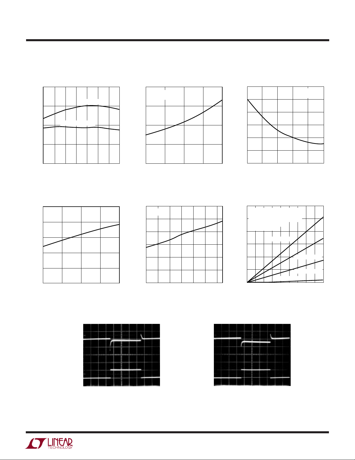
TYPICAL PERFOR A CE CHARACTERISTICS
Output Voltage vs
DAC Code
6
VCC = 5V
= 25°C
T
A
5
= 1mA
I
LOAD
4
3
2
OUTPUT VOLTAGE (V)
1
0
0
20 30 40
10
DAC CODE
50 60 63
1695 • G01
No Load Supply Current vs Supply
Voltage
250
TA = 25°C
200
150
100
SUPPLY CURRENT (µA)
50
0
4.0
4.5
5.0
SUPPLY VOLTAGE (V)
CODE 63
5.5
CODE 0
6.0
1695 • G02
No Load Supply Current vs
Temperature
3
Page 4
LTC1695
TEMPERATURE (°C)
–50
OUTPUT VOLTAGE (V)
4.95
4.93
4.91
4.89
4.87
4.85
0
50
75
1695 • G09
–25
25
100
125
VCC = 5V
CODE 63
I
LOAD
= 1mA
I
LOAD
= 150mA
CODE
0
INL (LSB)
0.25
0.15
0.05
–0.05
–0.15
–0.25
10
20 30 40
1695 • G12
50 60 63
VCC = 5V
I
LOAD
= 1mA
UW
TYPICAL PERFOR A CE CHARACTERISTICS
Ground Current (Dropout Mode) vs
Supply Voltage
900
TA =25°C
I
= 180mA
LOAD
800
700
600
GROUND CURRENT (µA)
500
400
4.0
4.5
SUPPLY VOLTAGE (V)
CODE 63
5.0
Output Voltage (Full Scale) vs
Load Current
4.930
4.920
4.910
4.900
4.890
OUTPUT VOLTAGE (V)
4.880
4.870
5.5
VCC = 5V
= 25°C
T
A
CODE 63
1695 • G04
6.0
Ground Current (Dropout Mode)
vs Temperature
900
VCC = 5V
= 180mA
I
LOAD
850
800
750
700
GROUND CURRENT (µA)
650
600
–50
–25 0
TEMPERATURE (°C)
CODE 63
50 100 125
25 75
Output Voltage (Midscale) vs Load
Current
2.505
2.500
2.495
2.490
OUTPUT VOLTAGE (V)
2.485
CODE 32
1695 • G05
VCC = 5V
= 25°C
T
A
Dropout Voltage vs
Load Current
175
VCC = 5V
150
125
100
75
50
DROPOUT VOLTAGE (mV)
25
0
0
TA = 25°C
40 8060 100 120 140 180160
20
LOAD CURRENT (mA)
TA = 85°C
TA = –40°C
Output Voltage (Full Scale) vs
Temperature
1695 • G06
4.860
2.510
2.505
2.500
2.495
2.490
OUTPUT VOLTAGE (V)
2.485
2.480
4
0
40 60 80 120100 140 180160
20
LOAD CURRENT (mA)
1695 • G07
2.480
0
20 60
40
80
LOAD CURRENT (mA)
100
120
180160140
1695 • G08
Output Voltage (Midscale) vs
Temperature Integral Nonlinearity (INL)
VCC = 5V
CODE 32
I
= 1mA
LOAD
I
= 150mA
LOAD
–50
–25 0
TEMPERATURE (°C)
50 100 125
25 75
1695 • G10
Differential Nonlinearity (DNL)
0.25
VCC = 5V
= 1mA
I
LOAD
0.15
0.05
DNL (LSB)
–0.05
–0.15
–0.25
0
20 30 40
10
CODE
50 60 63
1695 • G11
Page 5
UW
TYPICAL PERFOR A CE CHARACTERISTICS
Boost Start Timer vs Supply
POR and UVLO vs Temperature
3.00
POR (RISING VCC)
2.90
Voltage Boost Start Timer vs Temperature
350
TA = 25°C
= 10mA
I
LOAD
300
600
500
400
LTC1695
VCC = 5V
= 10mA
I
LOAD
2.80
SUPPLY VOLTAGE (V)
2.70
2.60
–50
UVLO (FALLING VCC)
–25 0 25 50
TEMPERATURE (°C)
Current Limit Threshold vs
Supply Voltage
425
TA = 25°C
400
375
350
CURRENT LIMIT (mA)
325
300
4.5
4.75
SUPPLY VOLTAGE (V)
5.0
5.25
10075 125
1695 • G13
5.5
1695 • G16
250
200
BOOST START TIMER (ms)
150
4.0
4.5
SUPPLY VOLTAGE (V)
Current Limit Threshold
vs Temperature
600
VCC = 5V
500
400
300
200
CURRENT LIMIT (mA)
100
0
–40
02040
–20
TEMPERATURE (°C)
5.0
5.5
1695 • G14
60 80 90
1695 • G17
300
200
BOOST START TIMER (ms)
100
6.0
120
100
80
60
40
20
JUNCTION TEMPERATURE INCREASE (°C)
0
0
0255075
–25
TEMPERATURE (°C)
Junction Temperature Increase
vs Load Current
VCC = 5V, TA = 25°C,
SOT-23 THERMAL RESISTANCE
= 150°C/W (PCB SOLDERED)
SEE APPLICATIONS
INFORMATION.
CODE 16 (1.25V)
CODE 32 (2.5V)
CODE 48 (3.75V)
CODE 63 (4.922V)
40 60 80 180
0 20 100 140 160
LOAD CURRENT (mA)
120
100
1695 • G15
1695 • G18
V
(AC)
OUT
20mV/DIV
I
LOAD
50mA/DIV
Load Transient Response
Code 32, 5mA to 55mA
V
= 5V
CC
= 4.7µF TANTALUM
C
OUT
100µs/DIV
1695 • G19
V
(AC)
OUT
10mV/DIV
I
LOAD
50mA/DIV
Load Transient Response
Code 32, 50mA to 100mA
V
= 5V
CC
C
= 4.7µF TANTALUM
OUT
100µs/DIV
1695 • G20
5
Page 6
LTC1695
1695 • G23
V
OUT
2V/DIV
100ms/DIV
V
CC
= 5V
C
IN
= 10µF
C
OUT
= 4.7µF
I
LOAD
= 1mA
UW
TYPICAL PERFOR A CE CHARACTERISTICS
V
(AC)
OUT
20mV/DIV
I
LOAD
50mA/DIV
Load Transient Response
Dropout (Code 63), 5mA to 55mA
V
= 5V
CC
= 4.7µF TANTALUM
C
OUT
100µs/DIV
1695 • G21
V
20mV/DIV
50mA/DIV
Load Transient Response
Dropout (Code 63), 50mA to 100mA
(AC)
OUT
I
LOAD
V
= 5V
CC
= 4.7µF TANTALUM
C
OUT
UUU
PIN FUNCTIONS
VCC (Pin 1): Power Supply Input. VCC supplies current to
the internal control circuitry, serves as the reference for
the 6-bit DAC and acts as the power path for the P-channel
low dropout linear regulator. Bypass V
with a low ESR capacitor ≥10µF.
GND (Pin 2): Ground. Tie GND to the ground plane.
SCL (Pin 3): SMBus Clock Input. Data is shifted into SDA
on the rising edge of the SCL clock signal during data
transfer.
directly to ground
CC
Boost Start Timer
100µs/DIV
1695 • G22
SDA (Pin 4): SMBus Bidirectional Data Input/Digital Output. SDA is an open drain output and requires a pull-up
resistor or current source to VCC. Data is shifted into SDA
and acknowledged by SDA.
V
(Pin 5): Linear Regulator Output. Connect directly to
OUT
the fan’s +VE terminal. V
is set to VZS (code 0) on
OUT
power-up. For good transient response and stability, use
a general purpose, low cost, medium ESR (0.1Ω to 1Ω)
tantalum or electrolytic capacitor. LTC recommends a
surface mount tantalum capacitor of ≥4.7µF.
6
Page 7

BLOCK DIAGRA
LTC1695
W
SCL
SDA
SHUTDOWN
CONTROL
THERMAL
SHUTDOWN
SMBus
INTERFACE
(BUFFERS,
LOGIC)
POWER ON
RESET
AND UVLO
BOOST START
TIMER
6-BIT DAC
(RESISTORS,
SWITCHES)
6
COMMAND
REGISTER
DATA
REGISTER
PULL-DOWN/UP
LOGIC
–
OP AMP
+
CURRENT
LIMIT
P1
0.75Ω
R1
50k
R2
50k
V
V
GND
1695 • BD
CC
OUT
7
Page 8

LTC1695
UW
SWITCHING WAVEFORMS
V
= V
OUT
FS
90% V
V
= V
OUT
ZS
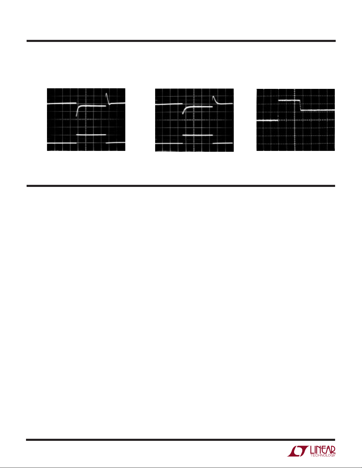
Boost Start Timer Measurement
I
LOAD
FS
= 10mA, C
t
BST_ST
LOAD
= 4.7µF
90% V
FS
V
= V(CODE 32)
OUT
1695 • SW01
Output Switch On Time Measurement
Code = 63, I
12 13 14 15 16 17 18 19
COMMAND BYTE
D5 D4 D3 D2 D1 D0
V
= V
OUT
FS
V
= V
OUT
ZS
LOAD
f
SMBus
= 1mA, C
=100kHz
CONDITION
ACK
STOP
LOAD
= 4.7µF
t
ON
90% V
FS
1695 • SW02
Output Switch Off Time Measurement
Code = 0, I
12 13 14 15 16 17 18 19
COMMAND BYTE
D5 D4 D3 D2 D1 D0
V
= V
OUT
FS
V
= V
OUT
ZS
= 150mA, C
LOAD
f
SMBus
=100kHz
CONDITION
ACK
STOP
LOAD
10% V
t
= 4.7µF
FS
OFF
1695 • SW03
8
Page 9

UWW
TI I G DIAGRA
LTC1695
Operating Sequence
SMBus SEND BYTE PROTOCOL, WITH SMBus ADDRESS = 1110100B
SCL
SDA
S = SMBus START BIT
P = SMBus STOP BIT
BST = 1 ENABLES THE BOOST START TIMER
D5 TO D0 = 6-BIT INPUT CODE FOR THE DAC (D5 = MSB)
X = DON'T CARE
SMBus RECEIVE BYTE PROTOCOL, WITH SMBus ADDRESS = 1110100B
SCL
SDA
S = SMBus START BIT
P = SMBus STOP BIT
OCF = 1 SIGNALS THAT THE LTC1695 IS IN CURRENT LIMIT
THE = 1 SIGNALS THAT THE LTC1695 IS IN THERMAL SHUTDOWN
Timing for SMBus Interface
PS
12 13 14 15 16 17 185678910111234 19
COMMAND BYTESLAVE ADDRESS
ACKWR0010111
D5 D4 D3 D2 D1 D0
12 13 14 15 16 17 185678910111234 19
COMMAND BYTESLAVE ADDRESS
ACKBSTX
PS
ACKTHEOCFACKWR0010000000111
1695 • TD01
SDA
SCL
STOP
t
HD(STA)
t
BUF
START
t
LOW
START
t
r
t
HD(DAT)
t
t
f
HIGH
t
SU(DAT)
t
HD(STA)
t
SU(STA)
t
STOP
SU(STO)
1695 • TD02
9
Page 10

LTC1695
DEFINITIONS
Resolution: The number of DAC output states (2N) that
divide the full-scale range. The resolution does not imply
linearity.
Full-Scale Voltage (VFS): The regulator output voltage
(V
) if all DAC bits are set to ones (code 63).
OUT
Voltage Offset Error (VOS): The regulator output voltage
if all DAC bits are set to zeros. The LDO amplifier can have
a true negative offset, but due to the LTC1695’s single
supply operation, V
offset is negative, V
cannot go below ground. If the
OUT
will remain near 0V resulting in the
OUT
transfer curve shown in Figure 1.
OUTPUT
VOLTAGE
NEGATIVE
0V
OFFSET
DAC CODE
Figure 1. Effect of Negative Offset
1695 • F01
Table 1. Nominal V
V
CC
4.5V 70.3mV 4.430V
5.0V 78.1mV 4.922V
5.5V 85.9mV 5.414V
LSB
and V
FS
V
LSB
values
V
FS
INL: Integral nonlinearity is the maximum deviation from
a straight line passing through the endpoints of the DAC
transfer curve. Due to the LTC1695’s single supply operation and the fact that V
cannot go below ground,
OUT
linearity is measured between full scale and the first code
(code 01) that guarantees a positive output. The INL error
at a given input code is calculated as follows:
INL = (V
V
IDEAL
V
= The output voltage of the DAC
OUT
– V
OUT
IDEAL
= (Code • V
LSB
))/V
) + V
LSB
OS
measured at the given input code
DNL: Differential nonlinearity is the difference between the
measured change and the ideal 1LSB change between any
two adjacent codes. The DNL error between any two codes
is calculated as below:
The offset of the part is measured at the first code (code␣ 1)
that produces an output voltage 0.5LSB greater than the
previous code.
V
= V
OS
Least Significant Bit (V
– [(Code • VFS)/(2N – 1)]
OUT
): The least significant bit or the
LSB
ideal voltage difference between two successive codes.
V
LSB
= (V
– VOS)/(2N – 1)
FS
DNL = (∆V
∆V
= The measured voltage difference
OUT
OUT
– V
LSB
)/V
LSB
between two adjacent codes
The ∆V
calculation includes the VOS values to account
OUT
for the effect of negative offset in Figure 1. This is relevant
for code 1’s DNL.
10
Page 11

LTC1695
U
WUU
APPLICATIONS INFORMATION
OVERVIEW
The LTC1695 is a 5V brushless DC fan speed controller.
Fan speed is controlled by linear regulating the applied
voltage to the fan. To program fan speed, a system
controller or microprocessor first sends a 6-bit digital
code to the LTC1695 via a 2-wire SMBus/I2C interface. The
LTC1695’s DAC then converts this digital code into a
voltage reference. Finally, the LTC1695’s op amp loop
regulates the gate bias of the internal P-channel pass
transistor to control the corresponding output voltage.
The LTC1695 is designed for portable, power-conscious
systems that utilize small 5V brushless DC fans. These
fans are increasingly popular in providing efficient cooling
solutions in a small footprint. Smaller fans allow a user to
employ multiple fans at strategic physical locations to
govern a system’s thermal airflow (“air duct” concept).
These brushless DC fans also make use of the 5V supply
used by the main digital/analog circuitry, removing the
need for a 12V supply required by higher power fans.
The LTC1695’s P-channel linear regulator control approach offers the lowest solution component count, the
smallest PCB board space consumed, wide fan speed
control range and low acoustical/electrical generated noise.
Thermal concerns over the use of a linear regulator topology are eliminated by the fan’s generally resistive behavior. As the LTC1695 DAC codes are changed to lower the
output voltage, the voltage across the internal P-channel
pass transistor increases. However, the fan’s load current
decreases almost linearly, thereby controlling power dissipation in the regulator. For example, a Micronel 5V, 0.7W
fan (40mm2 • 12mm) draws 80mA at 4V and 20mA at 2V.
Thus the P-channel pass transistor’s power loss decreases from 80mW to 60mW.
The LTC1695 incorporates several features to simplify the
overall solution including a boost start timer to ensure fan
start-up, output current limiting and thermal shutdown.
The boost start timer is enabled via the SMBus commands
and programs V
ing at the user programmed output voltage. This eliminates potential fan start-up problems at lower output
voltage DAC codes.
The LTC1695’s thermal shutdown circuit trips if die temperature exceeds 155°C. The P-channel pass transistor is
shut off and bit D6 in the LTC1695’s SMBus data register
is set high. If an overload or short-circuit condition occurs,
the LTC1695’s current-limit circuitry limits output current
to 390mA typically. In addition, bit D7 in the SMBus data
register is set high. The readback capability of the LTC1695
allows the host controller to monitor the status of the D6
and D7 bits for fault conditions.
SMBus Serial Interface
The LTC1695 is an SMBus slave device that supports both
SMBus send byte and receive byte protocol (Figure 2) with
two interface signals, SCL and SDA.
The SMBus host initiates communication with the LTC1695
through a start bit followed by a 7-bit address code and a
write bit. Each SMBus slave device in the system compares the address code with its specific address. For send
byte and receive byte protocol, the write bit is LOW and
HIGH respectively. If selected, the LTC1695 acknowledges by pulling SDA low.
If send byte protocol is used, the host issues an 8-bit
command code. After receiving the entire command byte,
the LTC1695 again acknowledges by pulling SDA low. At
the falling edge of the acknowledge pulse, the LTC1695’s
DAC latches in the new command byte from its shift
register.
If receive byte protocol is used, the LTC1695 acknowledges by pulling SDA low after the write bit. The LTC1695
then transmits the data byte. After the host receives the
entire data byte, the cycle is terminated by a “NOT Acknowledge” bit and a stop bit.
to full scale for 250ms before regulat-
OUT
11
Page 12

LTC1695
U
WUU
APPLICATIONS INFORMATION
SMBus SEND BYTE PROTOCOL
12345678910111213141516171819
S111010000X
A6 A5 A4 A3 A2 A1 A0 W A MSB LSB A
START STOP
SLAVE ADDRESS
12345678910111213141516171819
S1110100 01
A6 A5 A4 A3 A2 A1 A0 W A A
START STOP
SLAVE ADDRESS DATA BYTE
S = SMBus START BIT
P = SMBus STOP BIT
BST = 1 ENABLES THE BOOST START TIMER
D5 TO D0 = 6-BIT INPUT CODE FOR THE DAC (D5 = MSB)
OCF = 1 SIGNALS THAT THE LTC1695 IS IN CURRENT LIMIT
THE = 1 SIGNALS THAT THE LTC1695 IS IN THERMAL SHUTDOWN
BIT 18 = 1 IS A NOT ACKNOWLEDGE FOR RECEIVE BYTE PROTOCOL
NOTE: DURING POWER UP AND UVLO, DAC INPUT BITS
(D5 TO D0) AND THE BST BIT ARE RESET TO ZERO
Figure 2. SMBus Interface Bit Definition
SMBus RECEIVE BYTE PROTOCOL
BST
D5 D4 D3 D2 D1 D0 0 P
COMMAND BYTE
OCF THE
0000001P
1695 • F02
sistor capable of sinking 3mA at less than 0.4V during the
slave acknowledge sequence.
The LTC1695 is compatible with the Philips/Signetics I2C
Bus Interface. The 1.4V threshold for SCL and SDA does
not create any I2C application problems.
Early Stop Conditions
If a stop condition occurs before the data byte is acknowledged in the write byte protocol, the LTC1695’s DAC is not
updated. Otherwise, the internal register is updated with
the new data and V
changes accordingly to the new
OUT
programmed value.
Address, Command, Data Selection
The LTC1695’s address is hard-wired internally as 1110100
(MSB to LSB, A6 to A0). Consult LTC for parts with
alternate address codes. Consult the Address, Command
and Data Byte Tables for further information and as a
concise reference.
SCL and SDA
SCL is the synchronizing clock signal generated by the
host. SDA is the bidirectional data transfer line between
the host and a slave device. The host initiates a start bit by
pulling SDA from high to low while SCL is high. The stop
bit is initiated by changing SDA from low to high while SCL
is high. All address, command and acknowledge signals
must be valid and should not change while SCL is high.
The acknowledge bit signals to the host the acceptance of
a correct address byte or command byte.
The SCL and SDA input threshold voltages are typically
1.4V with 40mV of hysteresis. Connect the SCL and SDA
open-drain lines to either a resistive or current source pull
up. The LTC1695 SDA has an open-drain N-channel tran-
As shown in Figure 2, D5 to D0 in the command code,
control the linear regulator’s output voltage and thus fan
speed. D5 to D0 are sent from the host to the LTC1695
during send byte protocol. The LTC1695 latches D5 to D0
as DAC input data at the falling edge of the data acknowledge signal. The host must set “BST” (boost start enable
bit) to high if the LTC1695’s 250ms boost start timer
option is used. All bits are reset to zero during power-on
reset and UVLO. As shown in the Timing Diagram, bit 6
and bit 7 in the data byte register are defined as thermal
shutdown status (THE) and over current fault (OCF) status
respectively. The LTC1695 sets OCF high if I
LOAD
exceeds
390mA typically and “THE” high if junction temperature
exceeds 155°C typically. The remaining bits of the data
byte’s register (bit 5 to 0) are set low during host read
back.
12
Page 13

LTC1695
U
WUU
APPLICATIONS INFORMATION
V
CC
/2
V
CC
GND
64 RESISTOR
VOLTAGE TABS
Figure 3. Ladder DAC
720
SWITCHES
6
SMBus
COMMAND
D5 to D0
DAC
The LTC1695 uses a 128-segment resistor ladder to
implement the monotonic 6-bit voltage DAC (Figure 3).
Guaranteeing monotonicity (no missing codes) permits
the use of the LTC1695 in thermal feedback control
applications. As the typical application uses a 5V supply
for V
the reference for the 6-bit DAC is VCC. LTC
CC,
recommends a 10µF or greater tantalum capacitor to
bypass VCC. Users must account for the variation in the
DAC’s output absolute accuracy as V
should not exceed the absolute maximum rating of 7V or
drop below the typical 2.8V undervoltage lockout threshold (UVLO) during normal operation.
The LTC1695’s DAC specifications (INL, DNL, VOS) account for the offset and gain errors of the linear regulator
with respect to I
. Consult the Definitions section for
LOAD
more details.
The worst-case condition occurs if the LTC1695 P-chan-
nel pass transistor enters dropout at full-scale V
I
LOAD.
Full-scale V
(VFS) is 4.922V with VCC = 5V. In this
OUT
condition, loop gain drops and gain error increases. The
LTC1695 is designed for monotonicity up to V
and INL less than 0.75 LSB. Refer to the Electrical Characteristics and Typical Performance Characteristics for
more information.
REFERENCE
OP AMP
“000000” = 0V
“111111” = 0.984 • V
1695 • F03
varies. VCC voltage
CC
OUT
with DNL
FS
CC
and
/2
Linear Regulator Loop Compensation
The LTC1695’s linear regulator approach is a simple and
practical scheme for fan speed control featuring a wide and
linear dynamic range. It also introduces less noise into the
system supply rail, compared with a PWM scheme (fixed
frequency, variable duty cycle), switching regulator topology or simple ON-OFF control.
The LTC1695 linear regulator feedback loop requires a
capacitor at its output to stabilize the loop over the output
voltage and load current range. The output capacitor value
and the capacitor’s ESR value are critical in stabilizing the
LTC1695 feedback loop.
A ≥ 1 µF general purpose, low to medium ESR (0.1Ω to 5Ω)
tantalum or aluminium electrolytic capacitor is sufficient
for most applications. These capacitor types offer a lowcost advantage, particularly for fan speed control applications. As the output capacitance value increases, stability
improves. A typical 4.7µF, 1Ω ESR surface mount tanta-
lum capacitor is recommended for the optimum transient
response and frequency stability across temperature, V
and I
. Refer to the load transient response waveforms
LOAD
OUT
in the Typical Performance Characteristics section.
The selection of the capacitor for C
must be evaluated
OUT
by the user for temperature variation of the capacitance
and ESR value and the voltage coefficient of the capacitor
value. For example, the ESR of aluminium electrolytic
capacitors can increase dramatically at cold temperature.
Therefore, the regulator may be stable at room temperature but oscillate at cold temperature. Ceramic capacitors
with Z5U and Y5 dielectrics provide high capacitance
values in a small package, but exhibit strong voltage and
temperature coefficients (–80% in some cases). In addition, the ESR of surface mount ceramic capacitors is too
low (<0.1Ω) to provide adequate phase-lead in the feed-
back loop for stability.
Fan Load and C
Referring to Figure 4, C
LOAD
varies greatly depending on
LOAD
the type of fan used. The simplest, inexpensive fans
contain no protection circuitry and input capacitance is on
the order of 200pF. More expensive fans generally incorporate a series-diode for reverse protection and input
13
Page 14

LTC1695
U
WUU
APPLICATIONS INFORMATION
V
CC
INTERNAL
DAC
OUTPUT
capacitance ranges from 2pF to 30pF. As previously
discussed, an output bypass capacitor is required to
stabilize the feedback loop. This output capacitor is in
parallel with the fan’s input capacitance and dominates the
total capacitance. Thus, stability is generally not affected
by the fan’s input capacitance. The output capacitor also
serves to filter the fan’s output ripple during commutation
of the fan’s motor.
POR and UVLO
Under start-up conditions, the LTC1695 performs a power
on reset (POR) function. The digital logic circuitry is
disabled and the regulator is held off. The SMBus command register (to the DAC’s input) and data register
(current limit and thermal shutdown status) are reset to
zero. The POR signal deactivates if V
typically. The LTC1695 is then allowed to communicate
with the SMBus host and drive the fan accordingly. Upon
exiting POR, the regulator’s output voltage is set to V
(code 0) until programmed by the SMBus host.
The LTC1695 enters UVLO if VCC falls below 2.8V typically.
Between 2.8V and 1V, the digital logic circuitry is disabled,
the command/data registers are cleared and the regulator
is shut down. In general, 100mV of hysteresis exists
between the UVLO and POR thresholds.
–
OP AMP
C
GATE
+
+
+
C
NODE
Figure 4. Regulator Feedback Loop
P1(0.75Ω)
V
OUT
R1
ESR
R2
C
OUT
GND
+
rises above 2.9V
CC
EQUIVALENT
DC FAN CIRCUIT
L
FAN
+
C
FAN
1695 • F04
ZS
Thermal Considerations
The LTC1695’s power handling capability is limited by the
maximum rated junction temperature of 125°C. Power
dissipation (P
) consists of two components:
DISS
1. Output current multiplied by the input/output voltage
differential: (I
LOAD
)(V
CC
– V
OUT
), and
2. GND pin current multiplied by the input voltage:
(I
)(VCC).
GND
P
DISS
TJ = P
= (I
DISS
LOAD
• (θJA)
)(VCC – V
OUT
) + (I
GND
)(VCC)
The LTC1695 has active current limiting and thermal
shutdown circuitry for device protection during overload
or fault condition. For continuous overload conditions, do
not exceed the 125°C maximum junction temperature
T
. Give careful consideration to all thermal resis-
J(MAX)
tance sources from junction to ambient. Consider any
additional heat sources mounted in proximity to the
LTC1695. This is particularly relevant in applications
where the LTC1695’s output is loaded with a constant
I
LOAD
and V
is dynamically varied via the SMBus. At
OUT
lower DAC output voltage codes, the increased input-tooutput differential increases power dissipation if I
LOAD
does not decrease.
For the LTC1695’s 5-lead SOT-23 surface mount package,
heat sinking is accomplished by using the heat spreading
capabilities of the PC board and its copper traces (in
particular, the GND pin trace).
The following table lists measured thermal resistance
results for various size boards and copper areas. All
measurements were taken in still air on 3/32" FR-4 board
with one ounce copper.
Table 2. Measured Thermal Resistance (
Copper Area
Topside* Backside Board Area
2500mm22500mm
1000mm22500mm
225mm22500mm
100mm22500mm
50mm22500mm
*Device is mounted on topside
2
2
2
2
2
2500mm
2500mm
2500mm
2500mm
2500mm
θθ
θJA)
θθ
Thermal Resistance
(Junction to Ambient)
2
2
2
2
2
125°C/W
125°C/W
130°C/W
135°C/W
150°C/W
14
Page 15

LTC1695
U
WUU
APPLICATIONS INFORMATION
For further information, refer to the Junction Temperature
Increase (above ambient temperature) vs I
the Typical Performance Characteristics section. This
graph provides a fast and simple junction temperature
estimation with various V
combinations for a typical application.
Boost Start Timer
In general, a 5V brushless DC fan starts at a voltage value
higher than the voltage at which it stalls. This behavior is
directly attributed to the force necessary to overcome the
back EMF of the fan. For example, one fan measured
started at 3.5V but operated until its terminal voltage fell
below 2.1V. Therefore, users must ensure start-up in the
fan before programming the fan voltage to a value lower
than the starting voltage. Monitoring the fan’s DC current
for a stalled condition does not work due to the fan’s
resistive nature. Fans can sink load current even though
they are not rotating. Other approaches include detecting
absence of the fan’s commutation ripple current and
tachometers. In general, these approaches are more complex, require more circuitry, add cost and have to be
customized for the specific fan used.
The LTC1695 contains a programmable boost start timer
offering three flexible solutions to the user:
1.) Enable the boost start timer bit (D6 in the DAC command code). Each time a new output voltage is programmed, the timer forces V
nominal with V
programmed output voltage value. This ensures fan start
up even if the programmed output voltage is below the
fan’s start threshold.
2.) Users may also choose to use a software timer routine
inside the host controller to power the DC fan, at full scale,
for a programmed time period before programming V
to a lower desired DAC output voltage code.
3.) Users may choose a tachometer fan that feedbacks its
speed to the SMBus host. If fan stall conditions are
detected, the SMBus host re-programs the LTC1695.
Beyond a typical 125°C LTC1695 junction temperature,
the boost start timer (if activated) maintains V
= 5V) for 250ms before assuming the
CC
(DAC code) and I
OUT
to full scale (4.922V
OUT
LOAD
graph in
LOAD
OUT
at full
OUT
scale (VFS) until junction temperature decreases to
approximately 105°C. This extended timer period is an
attempt to cool down the system and the LTC1695 by
running the fan at full speed. In most cases, such elevated
ambient temperatures require the fan to run at full speed
anyway. The remaining LTC1695’s functionality remains
unchanged.
Thermal Shutdown, Overcurrent
The LTC1695 shuts down the P-channel linear regulator if
die temperature exceeds 155°C typically. The thermal
shutdown circuitry employs about 30°C of hysteresis. As
previously mentioned, the LTC1695 sets bit 6 (THE) in the
SMBus data byte register HIGH during thermal shutdown
conditions. During a fault condition, the LTC1695’s SMBus
logic continues to operate so that the SMBus host can read
back the fault status data.
During an overload or short-circuit fault condition, the
LTC1695’s current-limit detector sets bit 7 (OCF) in the
SMBus data byte register HIGH and actively limits output
current to 390mA typically. This protects the LTC1695’s
P-channel pass transistor. Under dead short conditions
with V
current. However, the increased power dissipation
(5V • 390mA = 1.95W) eventually forces the LTC1695 into
thermal shutdown. The LTC1695 will then thermally oscillate until the fault condition is removed.
During recovery from thermal shutdown (typically 125°C),
the LTC1695 automatically activates the boost start timer,
programming the fan voltage to full scale for 250ms
(T
BST_ST
put voltage value. This again eliminates fan start-up problems if the thermal shutdown fault occurred while the fan
was previously operating at an output voltage below the
fan’s starting voltage. In addition, as discussed, the boost
start timer will keep V
period beyond T
perature drops below 105°C.
The LTC1695’s protection features protect itself, the fan,
and more importantly alerts the SMBus host to any system
thermal management fault conditions.
= 0V, the LTC1695 also clamps the output
OUT
), before switching to the user programmed out-
at VFS for an extended time
OUT
until the LTC1695’s junction tem-
BST_ST
15
Page 16

LTC1695
U
WUU
APPLICATIONS INFORMATION
DC FAN SELECTION
The LTC1695, in the 5-lead SOT-23 package, caters mainly
to 5V brushless DC fans, in spot cooling and notebook
computer applications, that consume less than 1W maximum. These applications typically require fan footprints
on the order of 4000mm3 to 20000mm3. Such fan sizes
are common and commercially available. Examples of
these miniature fans are the “Ultra-thin DC fan” and
“Extra-mini DC fan” from SUNON Inc. Models in these
series range from 17mm to 40mm in size, weigh from 4
grams to 10 grams and provides airflow densities from
0.65 CFM to 6 CFM.
Users must consider parameters like physical size
(L • W • H), airflow (CFM), power dissipation (W) and
acoustically generated noise (dBA) when choosing a fan.
Users must also evaluate the fan’s I-V characteristics
versus fan speed and the start/stall characteristics of the
fan. Other factors include mechanical considerations such
as low cost sleeve bearings or ball bearings that have
better long term reliability. Finally, users must consider if
the fan requires any input protection features such as
reverse-voltage protection. All of these factors affect the
fan’s cost.
Table 4 lists some 5V brushless DC fans suitable for typical
LTC1695 fan speed control applications. Figure 5 shows
the measured I-V characteristics of these fans. For a
particular fan selection, users must determine the minimum DAC output voltage code below which the fan stalls.
Most fans continue to consume current, even in a stalled
condition.
Table 4. Some 5V DC Fans’ Characteristics
Manufacturer Part Number Airflow Power Size
(CFM) (W) (L • W • H)mm
SUNON KDE0501PFB2-8 0.65 0.50 20 • 20 • 10
ATC AD0205HB-G51 0.80 0.45 25 • 25 • 10
SUNON KDE0502PFB2-8 1.70 0.60 25 • 25 • 10
SUNON KDE0503PFB2-8 3.20 0.60 30 • 30 • 10
SUNON KDE0535PFB2-8 4.80 0.70 35 • 35 • 10
Micronel F41MM-005XK-9 6.10 0.70 40 • 40 • 12
150
125
100
KDE0501PFB2-8
KDE0535PFB2-8
KDE0502PFB2-8
AD0205HB-G51
KDE0503PFB2-8
F41MM-005XK-9
3
Table 3 lists some 5V fan manufacturer’s contact information.
Table 3. 5V DC Fan Manufacturers
Manufacturer Address
SUNON Inc. 1075 W. Lambert Rd., Brea, CA 92821
Tel: (714)255-0208
Website: http://www.sunon.com
Advanced Technology 1280 Liberty Way, Vista, CA 92083
Company Tel: (760)727-7430
Nidec America 152 Will Dr., Canton, MA 02021
Tel: (781)828-6216
Website: http://nidec.com
NMB Technologies Inc. 9730 Independence Ave., Chatsworth, CA 91311
Tel: (818)341-3355
Website: http://www.nmbtech.com
Micronel 1280 Liberty Way, Vista, CA 92083
Tel: (760)727-7400
Website: http://www.micronel.com
75
CURRENT (mA)
50
25
0
0
Figure 5. I-V Characteristics of 5V
Brushless DC Fan Samples
234
1
TERMINAL VOLTAGE (V)
TA = 25°C
5
1695 • F05
16
Page 17

LTC1695
U
WUU
APPLICATIONS INFORMATION
SMBus Address Byte Table
Decimal HEX SMBus Protocol
232 E8 Send Byte to the LTC1695
233 E9 Receive Byte from the LTC1695
The LSB of the SMBus address is the write bit. For send byte protocol,
W = 0. For Receive byte protocol, W = 1
SMBus Command Byte Table (Send Byte Protocol)
DECIMAL BINARY HEX Nominal V
(D5 to D0) MSB LSB (D6-D7 set to 0) I
0 X0000000 00 0.000
1 X0000001 01 0.078
2 X0000010 02 0.156
3 X0000011 03 0.234
4 X0000100 04 0.313
5 X0000101 05 0.391
6 X0000110 06 0.469
7 X0000111 07 0.547
8 X0001000 08 0.625
9 X0001001 09 0.703
10 X0001010 0A 0.781
11 X0001011 0B 0.859
12 X0001100 0C 0.938
13 X0001101 0D 1.016
14 X0001110 0E 1.094
15 X0001111 0F 1.172
16 X0010000 10 1.250
17 X0010001 11 1.328
18 X0010010 12 1.406
19 X0010011 13 1.484
20 X0010100 14 1.563
21 X0010101 15 1.641
22 X0010110 16 1.719
23 X0010111 17 1.797
24 X0011000 18 1.875
25 X0011001 19 1.953
26 X0011010 1A 2.031
27 X0011011 1B 2.109
28 X0011100 1C 2.188
29 X0011101 1D 2.266
30 X0011110 1E 2.344
31 X0011111 1F 2.422
D6 = 0 disables the boost start timer.
D7 = X = don’t care
LOAD
OUT
= 1mA
(V)
SMBus Data Byte Table (Receive Byte Protocol)
DECIMAL BINARY HEX LTC1695 Status
MSB LSB
0 00000000 00 No Fault
128 10000000 80 Overcurrent Fault/Clamp
64 01000000 40 Thermal Shutdown
During thermal shutdown, the LTC1695’s LDO is shut off.
DECIMAL BINARY HEX Nominal V
(D5 to D0) MSB LSB (D6-D7 set to 0) I
32 X0100000 20 2.500
33 X0100001 21 2.578
34 X0100010 22 2.656
35 X0100011 23 2.734
36 X0100100 24 2.813
37 X0100101 25 2.891
38 X0100110 26 2.969
39 X0100111 27 3.047
40 X0101000 28 3.125
41 X0101001 29 3.203
42 X0101010 2A 3.281
43 X0101011 2B 3.359
44 X0101100 2C 3.438
45 X0101101 2D 3.516
46 X0101110 2E 3.594
47 X0101111 2F 3.672
48 X0110000 30 3.750
49 X0110001 31 3.828
50 X0110010 32 3.906
51 X0110011 33 3.984
52 X0110100 34 4.063
53 X0110101 35 4.141
54 X0110110 36 4.219
55 X0110111 37 4.297
56 X0111000 38 4.375
57 X0111001 39 4.453
58 X0111010 3A 4.531
59 X0111011 3B 4.609
60 X0111100 3C 4.688
61 X0111101 3D 4.766
62 X0111110 3E 4.844
63 X0111111 3F 4.922
D6 = 0 disables the boost start timer.
D7 = X = don’t care
LOAD
OUT
= 1mA
(V)
17
Page 18

LTC1695
U
WUU
APPLICATIONS INFORMATION
SMBus Command Byte Table (Boost Start Timer Enabled)
DECIMAL BINARY HEX Nominal V
(D5 to D0) MSB LSB (D7 set to 0)
0 X1000000 40 0.000
1 X1000001 41 0.078
2 X1000010 42 0.156
3 X1000011 43 0.234
4 X1000100 44 0.313
5 X1000101 45 0.391
6 X1000110 46 0.469
7 X1000111 47 0.547
8 X1001000 48 0.625
9 X1001001 49 0.703
10 X1001010 4A 0.781
11 X1001011 4B 0.859
12 X1001100 4C 0.938
13 X1001101 4D 1.016
14 X1001110 4E 1.094
15 X1001111 4F 1.172
16 X1010000 50 1.250
17 X1010001 51 1.328
18 X1010010 52 1.406
19 X1010011 53 1.484
20 X1010100 54 1.563
21 X1010101 55 1.641
22 X1010110 56 1.719
23 X1010111 57 1.797
24 X1011000 58 1.875
25 X1011001 59 1.953
26 X1011010 5A 2.031
27 X1011011 5B 2.109
28 X1011100 5C 2.188
29 X1011101 5D 2.266
30 X1011110 5E 2.344
31 X1011111 5F 2.422
D6 = 1 enables the boost start timer.
D7 = X = don’t care
LOAD
OUT
= 1mA
(V)
DECIMAL BINARY HEX Nominal V
(D5 to D0) MSB LSB (D7 set to 0) I
32 X1100000 60 2.500
33 X1100001 61 2.578
34 X1100010 62 2.656
35 X1100011 63 2.734
36 X1100100 64 2.813
37 X1100101 65 2.891
38 X1100110 66 2.969
39 X1100111 67 3.047
40 X1101000 68 3.125
41 X1101001 69 3.203
42 X1101010 6A 3.281
43 X1101011 6B 3.359
44 X1101100 6C 3.438
45 X1101101 6D 3.516
46 X1101110 6E 3.594
47 X1101111 6F 3.672
48 X1110000 70 3.750
49 X1110001 71 3.828
50 X1110010 72 3.906
51 X1110011 73 3.984
52 X1110100 74 4.063
53 X1110101 75 4.141
54 X1110110 76 4.219
55 X1110111 77 4.297
56 X1111000 78 4.375
57 X1111001 79 4.453
58 X1111010 7A 4.531
59 X1111011 7B 4.609
60 X1111100 7C 4.688
61 X1111101 7D 4.766
62 X1111110 7E 4.844
63 X1111111 7F 4.922
D6 = 1 enables the boost start timer.
D7 = X = don’t care
LOAD
OUT
= 1mA
(V)
18
Page 19

PACKAGE DESCRIPTIO
LTC1695
U
Dimensions in inches (millimeters) unless otherwise noted.
S5 Package
5-Lead Plastic SOT-23
(LTC DWG # 05-08-1633)
2.80 – 3.00
(0.110 – 0.118)
(NOTE 3)
1.90
2.60 – 3.00
(0.102 – 0.118)
1.50 – 1.75
(0.059 – 0.069)
0.35 – 0.55
(0.014 – 0.022)
NOTE:
1. DIMENSIONS ARE IN MILLIMETERS
2. DIMENSIONS ARE INCLUSIVE OF PLATING
3. DIMENSIONS ARE EXCLUSIVE OF MOLD FLASH AND METAL BURR
4. MOLD FLASH SHALL NOT EXCEED 0.254mm
5. PACKAGE EIAJ REFERENCE IS SC-74A (EIAJ)
0.09 – 0.20
(0.004 – 0.008)
(NOTE 2)
(0.074)
REF
0.00 – 0.15
(0.00 – 0.006)
0.35 – 0.50
(0.014 – 0.020)
FIVE PLACES (NOTE 2)
0.95
(0.037)
REF
0.90 – 1.45
(0.035 – 0.057)
0.90 – 1.30
(0.035 – 0.051)
S5 SOT-23 0599
Information furnished by Linear Technology Corporation is believed to be accurate and reliable.
However, no responsibility is assumed for its use. Linear Technology Corporation makes no representation that the interconnection of its circuits as described herein will not infringe on existing patent rights.
19
Page 20

LTC1695
TYPICAL APPLICATION
U
TO
µC
10µF
6.3V
5V
LTC1695
1
V
C1
+
SCL
SDA
CC
2
GND
34
SCL
V
OUT
SDA
Output Voltage vs LED Current
20
18
16
14
12
10
8
LED CURRENT (mA)
6
4
2
0
0 0.5 1.0 1.5
SMBus I2C Controlled White LED Driver
5
R1
100Ω
LED1
LED = Hewlett Packard HLMP-CW30
C2 = SPRAGUE 595D106X0010A2T
2.0
3.0 3.5 4.0 4.5 5.0
2.5
OUTPUT VOLTAGE (V)
10µF
10V
+
C2
R2
100Ω
LED2
R3
100Ω
LED3
V
1695 • TA03b
R4
R5
100Ω
LED5
R6
100Ω
LED6
1695 • TA03a
100Ω
LED4
FS
RELATED PARTS
PART NUMBER DESCRIPTION COMMENTS
LT1120 125mA Low Dropout PNP Linear Regulator with 40µA 0.6V Dropout Voltage at 125mA
Quiescent Current
LT1121 150mA Low Dropout PNP Linear Regulator with 30µA 0.5V Dropout Voltage at 150mA, SO8/SOT-223 package
Quiescent Current
LTC1380/LTC1393 Single-Ended 8-Channel/Differential 4-Channel Analog Low RON: 35Ω Single-Ended/70Ω Differential,
Mux with SMBus Interface Expandable to 32 Single or 16 Differential Channels
LTC1427-50 Micropower, 10-Bit Current Output DAC Precision 50µA ± 2.5% Tolerance Over Temperature,
with SMBus Interface 4 Selectable SMBus Addresses, DAC Powers up at Zero or Midscale
LT1521 300mA Low Dropout PNP Linear Regulator with 12µA 0.5V Dropout Voltage at 150mA, SO8/SOT-223 Package
Quiescent Current
LTC1623 Dual High Side Switch Controller with SMBus Interface 8 Selectable Addresses/16-Channel Capability
LTC1663 SMBus Interface 10-Bit Rail-to-Rail Micropower DAC DNL < 0.75LBS Max, 5-Lead SOT-23 Package
LTC1694/LTC1694-1 SMBus Accelerator Improved SMBus/I2C Rise Time,
Ensures Data Integrity with Multiple SMBus/I
LT1761 100mA, Low Noise, LDO Micropower Regulator 0.3V Dropout Voltage at 100mA, SOT-23 Package
LT1762 150mA, Low Noise, LDO Micropower Regulator 0.3V Dropout Voltage at 150mA, MSOP Package
LT1786F SMBus Controlled CCFL Switching Regulator 1.25A, 200kHz, Floating or Grounded Lamp Configurations
Linear Technology Corporation
20
1630 McCarthy Blvd., Milpitas, CA 95035-7417
(408) 432-1900 ● FAX: (408) 434-0507
●
www.linear-tech.com
LINEAR TECHNOLOGY CORPORATION 2000
2
C Devices
1695f LT/TP 0400 4K • PRINTED IN USA
 Loading...