

Page 1
FEATURES
■
Improves SMBus/I2CTM Rise Time Transition
■
Ensures Data Integrity with Multiple Devices
on the SMBus/I2C
■
Improves Low State Noise Margin
■
Wide Supply Voltage Range: 2.7V to 6V
■
Tiny 5-Pin SOT-23 Package
■
Parallel Multiple LTC1694-1 Devices
for Increased Drive
U
APPLICATIO S
■
Notebook and Palmtop Computers
■
Portable Instruments
■
Battery Chargers
■
Industrial Control Application
■
TV/Video Products
■
ACPI SMBus Interface
LTC1694-1
SMBus/I2C Accelerator
U
DESCRIPTIO
The LTC®1694-1 is a dual SMBus active pull-up designed
to enhance data transmission speed and reliability under
all specified SMBus loading conditions. The LTC1694-1 is
also compatible with the Philips I2C Bus.
The LTC1694-1 allows multiple device connections or a
longer, more capacitive interconnect, without compromising slew rates or bus performance, by supplying a high
pull-up current of 2.2mA to slew the SMBus or I2C lines
during positive bus transitions
During negative transitions or steady DC levels, the
LTC1694-1 sources zero current. External resistors, one
on each bus line, trigger the LTC1694-1 during positive
bus transitions and set the pull-down current level. These
resistors determine the slew rate during negative bus
transitions and the logic low DC level.
The LTC1694-1 is available in a 5-pin SOT-23 package.
, LTC and LT are registered trademarks of Linear Technology Corporation.
I2C is a trademark of Philips Electronics N.V.
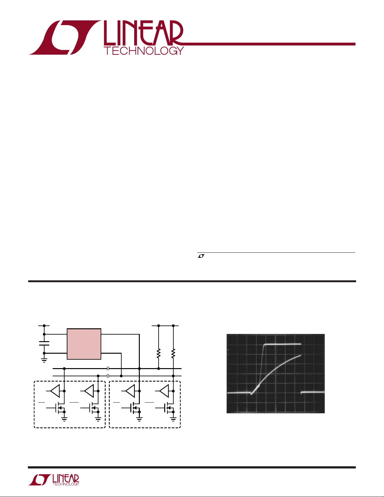
TYPICAL APPLICATIO
V
CC
5V
1
V
C1
0.1µF
2
GND
SCL
SMBus
SDA
CLK
IN
CLK
OUT
DEVICE 1
LTC1694-1: Patent Pending
DATA
DATA
CC
LTC1694-1
IN
OUT
SMBus1
SMBus2
5
4
CLK
IN
CLK
OUT
DEVICE N
U
V
CC
5V
DATA
DATA
OUT
Comparison of SMBus Waveforms for
the LTC1694-1 vs Resistor Pull-Up
R
R
P2
P1
IN
1694-1 TA01
LTC1694-1
1V/DIV
VCC = 5V 1µs/DIV 1694-1 TA02
CLD = 200pF
= 100kHz
f
SMBus
R
PULL-UP
= 15.8k
1
Page 2
LTC1694-1
VCC 1
GND 2
NC 3
5 SMBus1
4 SMBus2
TOP VIEW
S5 PACKAGE
5-LEAD PLASTIC SOT-23
WW
W
ABSOLUTE MAXIMUM RATINGS
(Note 1)
Supply Voltage (VCC) ................................................. 7V
SMBus1, SMBus2 Inputs ............ –0.3V to (VCC + 0.3V)
Operating Ambient Temperature Range....... 0°C to 70°C
U
U
W
PACKAGE/ORDER INFORMATION
ORDER PART
NUMBER
LTC1694-1CS5
Junction Temperature........................................... 125°C
Storage Temperature Range ................. –65°C to 150°C
S5 PART MARKING
Lead Temperature (Soldering, 10 sec.).................300°C
T
= 125°C, θJA = 256°C/W
JMAX
Consult factory for Industrial and Military grade parts.
ELECTRICAL CHARACTERISTICS
temperature range, otherwise specifications are at TA = 25°C. VCC = 2.7V to 6V, unless otherwise noted.
SYMBOL PARAMETER CONDITIONS MIN TYP MAX UNITS
V
CC
I
CC
I
PULL-UP
V
THRES
SR
THRES
t
r
f
MAX
Supply Voltage Range 2.7 6 V
Supply Current SMBus1 = SMBus2 = V
Pull-Up Current Positive Transition on SMBus ( Figure 1) ● 1.0 2.2 mA
Input Threshold Voltage Slew Rate = 0.5V/µs (Figure 1) ● 0.4 0.65 0.9 V
Slew Rate Detector Threshold SMBus > V
SMBus Rise Time Bus Capacitance = 200pF (Note 2) ● 0.32 1.0 µs
Standard Mode I
SMBus Maximum Operating Frequency (Note 4) ● 100 kHz
2
C Bus Rise Time Bus Capacitance = 400pF (Note 3) ● 0.30 1.0 µs
The ● denotes specifications which apply over the full operating
CC
Slew Rate = 0.5V/µs, SMBus > V
THRES
THRES
● 15 45 80 µA
● 0.2 0.5 V/µs
LTHE
U
Note 1: Absolute Maximum Ratings are those values beyond which the life
of a device may be impaired.
Note 2: The rise time of an SMBus line is calculated from (V
0.15V) to (V
guaranteed by design and not tested. With a minimum initial slew rate of
0.5V/µs, a minimum pull-up current of 1mA and a maximum input
threshold voltage of 0.9V:
2
–
+ 0.15V) or 0.65V to 2.25V. This parameter is
IH(MIN)
Rise Time = [(0.9V – 0.65V)/0.5V/µs] + [(2.25V – 0.9V) • 200pF/1mA]
= 0.77µs
IL(MAX)
Note 3: The rise time of an I2C bus line is calculated from V
or 1.5V to 3V (with VCC = 5V). This parameter is guaranteed by
V
IH(MIN)
design and not tested. With a minimum boosted pull-up current of 1mA:
Rise Time = (3V – 1.5V) • 400pF/1mA = 0.6µs
Note 4: This parameter is guaranteed by design and not tested.
IL(MAX)
to
Page 3
W
U
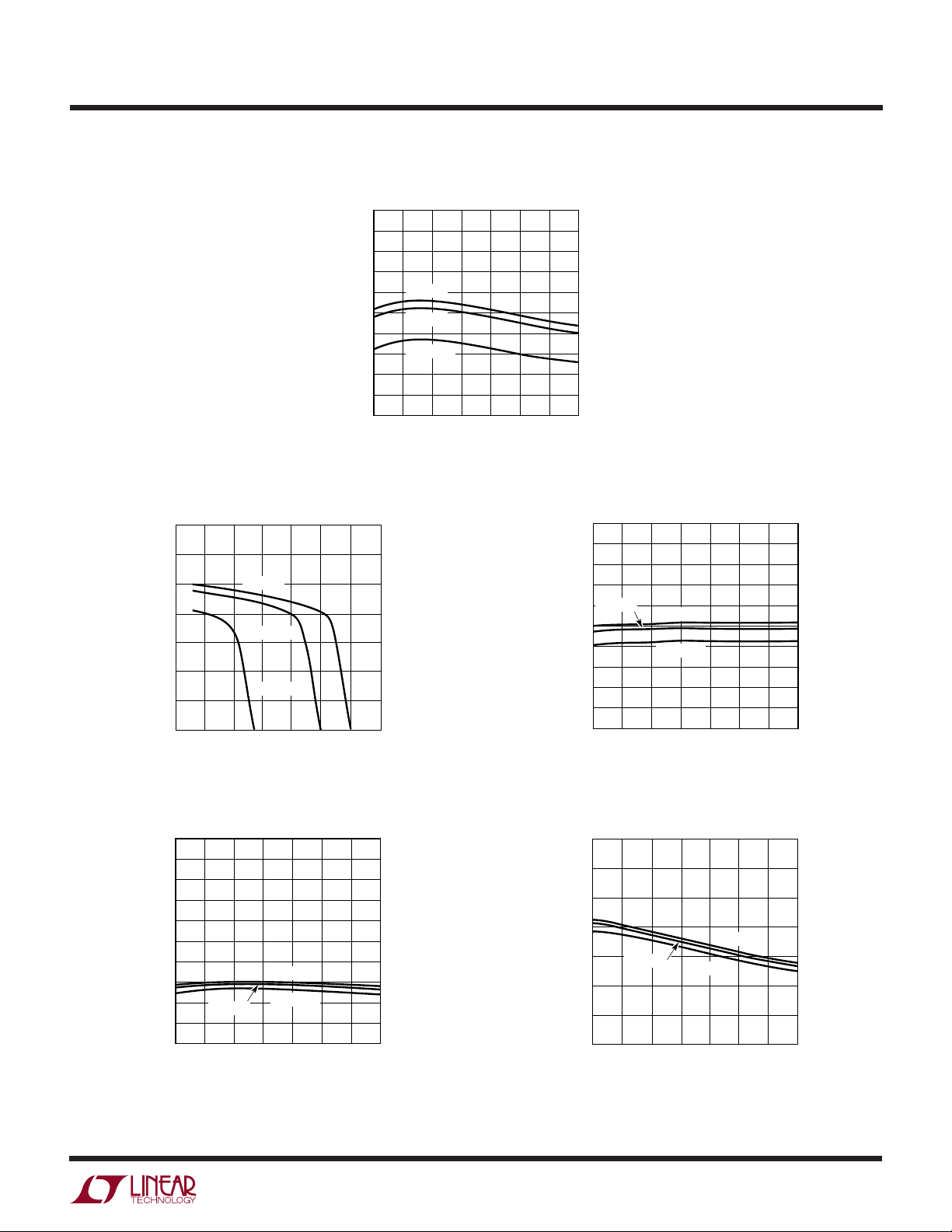
TYPICAL PERFORMANCE CHARACTERISTICS
Pull-Up Current
3.50
3.25
3.00
2.75
–50
VCC = 6V
VCC = 5V
VCC = 2.7V
0
–25
TEMPERATURE (°C)
50
25
75
100
1694-1 G01
Pull-Up Current
vs SMBus Voltage
3.5
3.0
2.5
2.0
1.5
1.0
PULL-UP CURRENT (mA)
0.5
0
0
12
SMBus VOLTAGE (V)
VCC = 6V
VCC = 5V
VCC = 2.7V
467
35
2.50
2.25
2.00
1.75
PULL-UP CURRENT (mA)
1.50
1.25
1.00
LT1694 G02
125
Input Threshold Voltage
0.90
0.85
0.80
0.75
VCC = 5V
0.70
0.65
0.60
0.55
0.50
INPUT THRESHOLD VOLTAGE (V)
0.45
0.40
–50
–25
VCC = 6V
VCC = 2.7V
0
25
TEMPERATURE (°C)
LTC1694-1
50
75
100
125
1694 G03
Slew Rate Detector Threshold
0.50
0.45
0.40
0.35
0.30
0.25
SLEW RATE DETECTOR THRESHOLD (V/µs)
0.20
0.15
0.10
0.05
0
–50
VCC = 5V
–25
VCC = 6V
VCC = 2.7V
0
TEMPERATURE (°C)
50
25
Standby Mode Supply Current
80
70
60
50
40
30
SUPPLY CURRENT (µA)
20
100
125
1694 G04
75
10
VCC = 5V
–25 25 75 125
–50
050
TEMPERATURE (°C)
VCC = 6V
VCC = 2.7V
100
1694-1 G05
3
Page 4

LTC1694-1
PULL-UP =
2.2mA (TYP)
200µA
(TYP)
TEST RAMP
VOLTAGE
0µA
V
CC
1694-1 F01b
0.5V/µs
0V
V
THRES
I
PULL-UP
=
V
R
1kΩ
UUU
PIN FUNCTIONS
VCC (Pin 1): Power Supply Input. VCC can range from 2.7V
to 6V and requires a 0.1µF bypass capacitor to GND.
Supply current is typically 45µA when the SMBus or I2C
lines are inactive (SCL and SDA are a logic high level).
GND (Pin 2): Ground.
W
BLOCK DIAGRAM
V
CC
1
2.2mA
SMBus1
5
GND
2
0.65V
V
REF
NC (Pin 3): No Connection.
SMBus2 (Pin 4): Active pull-up for SMBus.
SMBus1 (Pin 5): Active pull-up for SMBus.
CHANNEL ONE
SLEW RATE
DETECTOR
CONTROL
LOGIC
+
VOLTAGE
COMP
–
TEST CIRCUITS
V
5V
C1
0.1µF
TEST RAMP VOLTAGE
SMBus2
4
V
CC
CC
V
CC
LTC1694-1
GND
SMBus1
SMBus2
5
4
5V
200µA
HP5082-2080
(DUPLICATE OF CHANNEL ONE)
CHANNEL TWO
1694-1 BD
–
LT®1360
BSS284
+
V
R
1k
–10V
1694-1 F01a
4
Figure 1
Page 5

LTC1694-1
U
WUU
APPLICATIONS INFORMATION
SMBus Overview
SMBus communication protocol employs open-drain
drives with resistive or current source pull-ups. This protocol allows multiple devices to drive and monitor the bus
without bus contention. The simplicity of resistive or fixed
current source pull-ups is offset by the slow rise times
resulting when bus capacitance is high. Rise times can be
improved by using lower pull-up resistor values or higher
fixed current source values, but the additional current
increases the low state bus voltage, decreasing noise
margins. Slow rise times can seriously impact data reliability, enforcing a maximum practical bus speed well
below the established SMBus maximum transmission rate.
Theory of Operation
The LTC1694-1 overcomes these limitations by providing
a 2.2mA pull-up current only during positive bus transitions to quickly slew any bus capacitance. Therefore, rise
time is dramatically improved, especially with maximum
SMBus loading conditions.
The LTC1694-1 has separate but identical circuitry for
each SMBus output pin. The circuitry consists of a positive
edge slew rate detector and a voltage comparator.
For I/O stage protection from ESD and high voltage spikes
on the SMBus, a series resistor RS (Figure 2) is sometimes
added to the open-drain driver of the bus agents. This is
especially common in SMBus-controlled smart batteries.
Both the values of RP and RS must be chosen carefully to
meet the low state noise margin and all timing requirements of the SMBus.
A discussion of the electrical parameters affected by the
values of RS and RP, as well as a general procedure for
selecting the values of RS and RP follows.
V
CC
R
P
SMBus
C
BUS
DATA
DATA
OUT
R
S
IN
R
ON
1694-1 F02
Figure 2
The 2.2mA pull-up current is only turned on if the voltage
on the SMBus line voltage is greater than the 0.65V
comparator threshold voltage and the positive slew rate of
the SMBus line is greater than the 0.2V/µs threshold of the
slew rate detector. The pull-up current remains on until the
voltage on the SMBus line is within 0.5V of VCC and/or the
slew rate drops below 0.2V/µs.
Selecting the Values of RS and R
P
An external pull-up resistor RP is required in each SMBus
line to supply a steady state pull-up current if the SMBus
is at logic zero. This pull-up current is used for slewing the
SMBus line during the initial portion of the positive transition in order to activate the LTC1694-1 2.2mA pull-up
current.
Using an external RP to supply the steady state pull-up
current permits the user the freedom to adjust rise time
versus fall time as well as defining the low state logic level
(VOL).
Low State Noise Margin
A low value of VOL, the low state logic level, is desired for
good noise margin. VOL is calculated as follows:
VOL = (RL • VCC)/(RL + RP) (1)
RL is the series sum of RS and RON, the on-resistance of
the open-drain driver.
Increasing the value of RP decreases the value of VOL.
Increasing RL increases the value of VOL.
Initial Slew Rate
The initial slew rate, SR, of the Bus is determined by:
SR = (V
SR must be greater than SR
– VOL)/(RP • C
CC
) (2)
BUS
, the LTC1694-1 slew
THRES
rate detector threshold (0.5/µs max) in order to activate
the 2.2mA pull-up current.
5
Page 6

LTC1694-1
U
WUU
APPLICATIONS INFORMATION
SMBus Rise Time
Rise time of an SMBus line is derived using equations 3,
4 and 5.
tr = t1 + t
t1 = –RP • C
(V
if (V
ILMAX
t2 = –RP • C
(RP • I
2
• ln[(V
BUS
– 0.15 – VCC)] (4)
ILMAX
– 0.15) > V
PULL-UP
BUS
)]/[V
THRES
• ln{[V
THRES
– VCC)/
THRES
, then t1 = 0µs.
+ 0.15 – VCC –
IHMIN
– VCC – (RP • I
PULL-UP
By ignoring the current through RP, a simplified version
of equation 3 is obtained:
t2 = (V
For an SMBus system, V
For the LTC1694-1, typically V
IHMIN
+ 0.15 – V
) • C
THRES
= 0.8V and V
ILMAX
THRES
BUS/IPULL-UP
IHMIN
= 0.65V and I
= 2.2mA.
(3)
)]} (5)
(6)
= 2.1V.
PULL-UP
For an I2C system with VCC related input levels, V
0.3VCC and V
C
is the total capacitance of the I2C line.
BUS
IHMIN
= 0.7VCC.
ILMAX
=
A general procedure for selecting RP and RL is as follows:
1. RL is first selected based on the I/O protection requirement. Generally, an RS of 100Ω is sufficient for high
voltage spike and ESD protection. RON is determined by
the size of the open-drain driver, a large driver will have
a lower RON.
2. Next, the value of RP is determined based on the rise and
fall time requirements using equations 3 to 7 (for an
SMBus system) or 8 and 9 (for an I2C system). The
value chosen for RP must ensure that both the rise and
fall time specifications are met simultaneously.
3. After RP and RL are selected, use equations 1 and 2 to
check if the VOL and SR requirements are fulfilled.
C
is the total capacitance of the SMBus line.
BUS
Increasing the value of RP increases the rise time.
SMBus Fall Time
Fall time of an SMBus line is derived using equation 7:
tf = RT • C
[(V
ILMAX
• ln{[0.9 • (RP + RL) – RL]/
BUS
– 0.15) • (RP + RL)/VCC – RL]} (7)
where RT is the parallel equivalent of RP and RL.
The rise and fall time calculation for an I2C system is as
follows.
I2C Bus Rise and Fall Time
Rise time of an I2C line is derived using equation 8.
tr = –RP • C
[V
– VCC – (RP • I
ILMAX
BUS
• ln{[V
– VCC – (RP • I
IHMIN
PULL-UP
)]} (8)
PULL-UP
)]/
Fall time of an I2C line is derived using equation 9:
tf = RT • C
[(V
ILMAX/VCC
For an I2C system with fixed input levels, V
and V
IHMIN
BUS
• ln{[(V
IHMIN/VCC
) • (RP + RL) – RL]/
) • (RP + RL) – RL]} (9)
ILMAX
= 3V.
= 1.5V
If SR is too low, decrease the value of RP. If VOL is too high,
increase the value of RP.
SMBus Design Example
Given the following conditions and requirements:
VCC = 3.3V nom
VOL = 0.4V max
C
= 200pF max
BUS
V
ILMAX
= 0.8V, V
IHMIN
= 2.1V
tr = 0.8µs max, tf = 0.3µs max
If an RS of 500Ω is used and the max RON of the driver
is 200Ω, then RL = 500 + 200 = 700Ω. Using the max
V
of 0.9V and a min I
THRES
PULL-UP
of 1mA.
Using equation 6 to calculate the approximate value of t2:
t2 = (2.1 + 0.15 – 0.9) • [(200 • 10
–12
)/(1 • 10–3)]
= 0.27µs
t1 = 0.8 – 0.27 = 0.53µs
Using equation 4 to find the required RP to meet tr:
RP = –t1/{C
(V
– 0.15 – VCC)]} = 27k
ILMAX
BUS
• ln[(V
THRES
– VCC)/
RT = (RP • RL)/(RP + RL)
6
Page 7

LTC1694-1
U
WUU
APPLICATIONS INFORMATION
Using equations 4 and 5 to check exact value of tr:
tr = 0.535µs + 0.254µs = 0.79µs
Using equation 7 to check tf:
tf = 0.222µs
which is less than 0.3µs.
Using equation 1 to check VOL:
VOL = (3.3 • 700)/[700 + (27 • 103)] = 83mV
which is less than 0.4V.
And using equation 2 to check the initial slew rate:
SR = 3.3/[(27 • 103) • (200 • 10
which is greater than 0.5V/µs.
Therefore, the value of RP chosen is 27k.
ACK Data Setup Time
Care must be taken in selecting the value of RS (in series
with the pull-down driver) to ensure that the data setup
time requirement for ACK (acknowledge) is fulfilled. An
acknowledge is accomplished by the SMBus host releasing the SDA line (pulling high) at the end of the last bit sent
and the SMBus slave device pulling the SDA line low
before the rising edge of the ACK clock pulse.
–12
)] = 0.61V/µs
The LTC1694-1 2.2mA pull-up current is activated when
the SMBus host releases the SDA line, allowing the
voltage to rise above the LTC1694-1’s comparator threshold of 0.65V. If an SMBus slave device has a high value
of RS, a longer time is required for this SMBus slave
device to pull SDA low before the rising edge of the ACK
clock pulse.
To ensure sufficient data setup time for ACK, SMBus slave
devices with high values of RS, should pull the SDA low
earlier. Typically, a minimum setup time of 1.5µs is needed
for an SMBus device with an RS of 700Ω and a bus
capacitance of 200pF.
An alternative is that the SMBus slave device can hold SCL
line low until the SDA line reaches a stable state. Then, SCL
can be released to generate the ACK clock pulse.
Connecting Multiple LTC1694-1 in Parallel
The LTC1694-1 is designed to guarantee a maximum
SMBus rise time of 1µs with a bus capacitance of 200pF.
In some cases where the bus capacitance is higher than
200pF, multiple LTC1694-1s can be connected in parallel
to provide a higher pull-up current to meet the rise time
requirement. Figure 3 shows a typical application with two
LTC1694-1s connected in parallel to supply a pull-up
current of 4.4mA.
SMBus
V
CC
5V
SCL
SDA
5
SMBus1
4
SMBus2
CLK
IN
CLK
OUT
DEVICE 1
LTC1694-1
V
GND
1
CC
2
DATA
IN
DATA
OUT
C1
0.1µF
1
2
V
CC
LTC1694-1
GND
SMBus1
SMBus2
CLK
CLK
OUT
DEVICE N
5
4
IN
Figure 3. Paralleling Two LTC1694-1 to Provide 4.4mA of Pull-Up Current
Information furnished by Linear Technology Corporation is believed to be accurate and reliable.
However, no responsibility is assumed for its use. Linear Technology Corporation makes no representation that the interconnection of its circuits as described herein will not infringe on existing patent rights.
DATA
DATA
OUT
R
R
P2
P1
IN
1694-1 f03
7
Page 8

LTC1694-1
U
WUU
APPLICATIONS INFORMATION
Comparison of SMBus Waveforms for the LTC1694-1 vs Resistor Pull-Up
LTC1694-1
1V/DIV
VCC = 5V 1µs/DIV
= 200pF
C
LD
f
= 100kHz 1694 TA03
SMBus
R
PULL-UP
= 15.8k
U
PACKAGE DESCRIPTION
Dimensions in inches (millimeters) unless otherwise noted.
LTC1694-1
1V/DIV
VCC = 3.3V 1µs/DIV
= 200pF
C
LD
f
= 100kHz 1694 TA04
SMBus
R
PULL-UP
= 10.5k
S5 Package
5-Lead Plastic SOT-23
(LTC DWG # 05-08-1633)
2.60 – 3.00
(0.102 – 0.118)
1.50 – 1.75
(0.059 – 0.069)
0.35 – 0.55
(0.014 – 0.022)
NOTE:
1. DIMENSIONS ARE IN MILLIMETERS
2. DIMENSIONS ARE INCLUSIVE OF PLATING
3. DIMENSIONS ARE EXCLUSIVE OF MOLD FLASH AND METAL BURR
4. MOLD FLASH SHALL NOT EXCEED 0.254mm
5. PACKAGE EIAJ REFERENCE IS SC-74A (EIAJ)
0.09 – 0.20
(0.004 – 0.008)
(NOTE 2)
0.00 – 0.15
(0.00 – 0.006)
0.35 – 0.50
(0.014 – 0.020)
FIVE PLACES (NOTE 2)
0.90 – 1.45
(0.035 – 0.057)
0.90 – 1.30
(0.035 – 0.051)
2.80 – 3.00
(0.110 – 0.118)
(NOTE 3)
(0.074)
1.90
REF
0.95
(0.037)
REF
S5 SOT-23 0599
RELATED PARTS
PART NUMBER DESCRIPTION COMMENTS
LTC1380/LTC1393 8-Channel/4-Channel Analog Multiplexer with SMBus interface Low RON and Low Charge Injection
LTC1427 10-Bit Current DAC with SMBus Interface 50µA Full-Scale Current
LTC1623 Dual High Side Switch Controller with SMBus Interface 8 Selectable Addresses/16 Channel Capability
LTC1663 SMBus Interface 10-Bit Rail-to-Rail Micropower DAC DNL < 0.75LSB Max, 5-Lead SOT-23 Package
LTC1694 SMBus Accelerator Includes DC and AC Pull-Up Current
LT1786F SMBus-Controlled CCFL Switching Regulator 1.25A, 200kHz, Floating or Grounded Lamp Configurations
8
Linear Technology Corporation
1630 McCarthy Blvd., Milpitas, CA 95035-7417
(408) 432-1900 ● FAX: (408) 434-0507
●
www.linear-tech.com
16941f LT/TP 1099 4K • PRINTED IN USA
LINEAR TECHNOLOGY CORPORATION 1999
 Loading...