

Page 1
FEATURES
LTC1690
Differential Driver and
Receiver Pair with Fail-Safe
Receiver Output
U
DESCRIPTIO
■
No Damage or Latchup to ±15kV ESD (Human Body
Model), IEC1000-4-2 Level 4 (±8kV) Contact and
Level 3 (±8kV) Air Discharge
■
Guaranteed High Receiver Output State for
Floating, Shorted or Terminated Inputs with No
Signal Present
■
Drives Low Cost Residential Telephone Wires
■
ICC = 600µA Max with No Load
■
Single 5V Supply
■
–7V to 12V Common Mode Range Permits ±7V
Ground Difference Between Devices on the Data Line
■
Power-Up/Down Glitch-Free Driver Outputs Permit
Live Insertion or Removal of Transceiver
■
Driver Maintains High Impedance with the Power Off
■
Up to 32 Transceivers on the Bus
■
Pin Compatible with the SN75179 and LTC490
■
Available in SO, MSOP and PDIP Packages
U
APPLICATIO S
■
Battery-Powered RS485/RS422 Applications
■
Low Power RS485/RS422 Transceiver
■
Level Translator
■
Line Repeater
The LTC®1690 is a low power receiver/driver pair that is
compatible with the requirements of RS485 and RS422.
The receiver offers a fail-safe feature that guarantees a
high receiver output state when the inputs are left open,
shorted together or terminated with no signal present. No
external components are required to ensure the high
receiver output state.
Separate driver output and receiver input pins allow full
duplex operation. Excessive power dissipation caused by
bus contention or faults is prevented by a thermal shutdown circuit which forces the driver outputs into a high
impedance state.
The LTC1690 is fully specified over the commercial and
industrial temperature ranges. The LTC1690 is available in
8-Pin SO, MSOP and PDIP packages.
, LTC and LT are registered trademarks of Linear Technology Corporation.
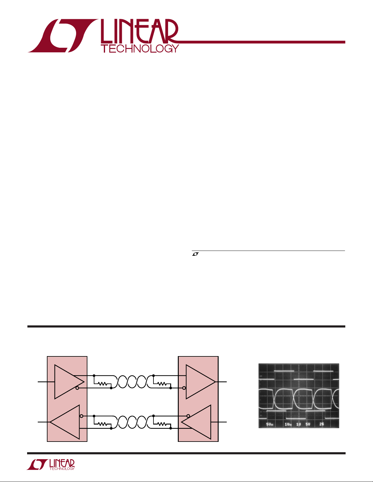
TYPICAL APPLICATIO
LTC1690 LTC1690
5
Y1
3
D1
2
R1
120Ω
6
Z1
7
B1
120Ω
8
A1
U
120Ω
120Ω
Driving a 1000 Foot STP Cable
8
A2
2
RECEIVER
7
B2
Z2
6
5
Y2
1690 TA01
R2DRIVER
3
D2RECEIVER DRIVER
D1
B2
A2
R2
1690 TA01a
1
Page 2
LTC1690
1
2
3
4
8
7
6
5
TOP VIEW
MS8 PACKAGE
8-LEAD PLASTIC MSOP
V
CC
R
D
GND
A
B
Z
Y
WW
W
ABSOLUTE MAXIMUM RATINGS
U
(Note 1)
Supply Voltage (VCC) .............................................. 6.5V
Driver Input Voltage..................... –0.3V to (VCC + 0.3V)
Driver Output Voltages ................................. –7V to 10V
Receiver Input Voltages ......................................... ±14V
Receiver Output Voltage .............. –0.3V to (VCC + 0.3V)
Junction Temperature........................................... 125°C
U
W
PACKAGE/ORDER INFORMATION
ORDER PART
NUMBER
LTC1690CMS8
T
JMAX
= 125°C, θ
= 200°C/W
JA
MS8 PART MARKING
LTDA
Operating Temperature Range
LTC1690C ........................................ 0°C ≤ TA ≤ 70°C
LTC1690I..................................... – 40°C ≤ TA ≤ 85°C
Storage Temperature Range ................. –65°C to 150°C
Lead Temperature (Soldering, 10 sec).................. 300°C
U
ORDER PART
V
1
CC
R
2
D
3
GND
4
S8 PACKAGE
8-LEAD PLASTIC SO
T
= 125°C, θ
JMAX
= 125°C, θ
T
JMAX
TOP VIEW
R
D
N8 PACKAGE
8-LEAD PLASTIC DIP
= 130°C/W (N)
JA
= 135°C/W (S)
JA
A
8
B
7
Z
6
Y
5
NUMBER
LTC1690CN8
LTC1690IN8
LTC1690CS8
LTC1690IS8
S8 PART MARKING
1690
1690I
DC ELECTRICAL CHARACTERISTICS
Consult factory for Military Grade Parts
The ● denotes the specifications which apply over the full operating
temperature range, otherwise specifications are at T
SYMBOL PARAMETER CONDITIONS MIN TYP MAX UNITS
V
OD1
V
OD2
V
OD3
∆V
V
OC
∆|VOC| Change in Magnitude of Driver Common Mode R = 22Ω, 27Ω or 50Ω, Figure 1 ● 0.2 V
V
IH
V
IL
I
IN1
I
IN2
V
TH
∆V
2
Differential Driver Output Voltage (Unloaded) IO = 0 ● V
Differential Driver Output Voltage (with Load) R = 50Ω; (RS422) ● 2V
Differential Driver Output Voltage (with Common Mode) V
Change in Magnitude of Driver Differential Output R = 22Ω, 27Ω or 50Ω, Figure 1 ● 0.2 V
OD
Voltage for Complementary Output States V
Driver Common Mode Output Voltage R = 22Ω, 27Ω or 50Ω, Figure 1 ● 3V
Output Voltage for Complementary Output States
Input High Voltage Driver Input (D) ● 2V
Input Low Voltage Driver Input (D) ● 0.8 V
Input Current Driver Input (D) ● ±2 µA
Input Current (A, B) VCC = 0V or 5.25V, VIN = 12V ● 1mA
Differential Input Threshold Voltage for Receiver –7V ≤ VCM ≤ 12V ● –0.20 –0.01 V
Receiver Input Hysteresis VCM = 0V ±30 mV
TH
= 25°C. VCC = 5V ±5% (Notes 2, 3)
A
R = 22Ω or 27Ω; (RS485), Figure 1
= –7V to 12V, Figure 2 1.5 5 V
TST
= –7V to 12V, Figure 2
TST
= 0V or 5.25V, VIN = –7V ● –0.8 mA
V
CC
CC
● 1.5 5 V
V
Page 3
LTC1690
DC ELECTRICAL CHARACTERISTICS
temperature range, otherwise specifications are at T
= 25°C. VCC = 5V ±5% (Notes 2, 3)
A
The ● denotes the specifications which apply over the full operating
SYMBOL PARAMETER CONDITIONS MIN TYP MAX UNITS
V
OH
V
OL
R
IN
I
CC
I
OSD1
I
OSD2
I
OZ
I
OSR
t
PLH
t
PHL
t
SKEW
tr, t
t
PLH
t
PHL
t
SKD
f
MAX
Note 1: Absolute Maximum Ratings are those values beyond which the life
of the device may be impaired.
Receiver Output High Voltage IO = –4mA, VID = 200mV ● 3.5 V
Receiver Output Low Voltage IO = 4mA, VID = –200mV ● 0.4 V
Receiver Input Resistance –7V ≤ VCM ≤ 12V ● 12 22 kΩ
Supply Current No Load ● 260 600 µA
Driver Short-Circuit Current, V
Driver Short-Circuit Current, V
= HIGH –7V ≤ VO ≤ 10V 35 250 mA
OUT
= LOW –7V ≤ VO ≤ 10V 35 250 mA
OUT
Driver Three-State Current (Y, Z) –7V ≤ VO ≤ 10V, VCC = 0V ● 5 200 µA
Receiver Short-Circuit Current 0V ≤ VO ≤ V
Driver Input to Output, Figure 3, Figure 4 R
Driver Input to Output, Figure 3, Figure 4 R
Driver Output to Output, Figure 3, Figure 4 R
Driver Rise or Fall Time, Figure 3, Figure 4 R
f
Receiver Input to Output, Figure 3, Figure 5 R
Receiver Input to Output, Figure 3, Figure 5 R
|t
– t
PLH
|, Differential Receiver Skew, Figure 3, Figure 5 R
PHL
Maximum Data Rate, Figure 3, Figure 5 R
CC
= 54Ω, CL1 = CL2 = 100pF ● 10 22.5 60 ns
DIFF
= 54Ω, CL1 = CL2 = 100pF ● 10 25 60 ns
DIFF
= 54Ω, CL1 = CL2 = 100pF ● 2.5 15 ns
DIFF
= 54Ω, CL1 = CL2 = 100pF ● 21340 ns
DIFF
= 54Ω, CL1 = CL2 = 100pF ● 30 94 160 ns
DIFF
= 54Ω, CL1 = CL2 = 100pF ● 30 89 160 ns
DIFF
= 54Ω, CL1 = CL2 = 100pF 5 ns
DIFF
= 54Ω, CL1 = CL2 = 100pF ● 5 Mbps
DIFF
● 785mA
Note 2: All currents into device pins are positive; all currents out of device
pins are negative. All voltages are referenced to device ground unless
otherwise specified.
Note 3: All typicals are given for V
= 5V and TA = 25°C.
CC
UW
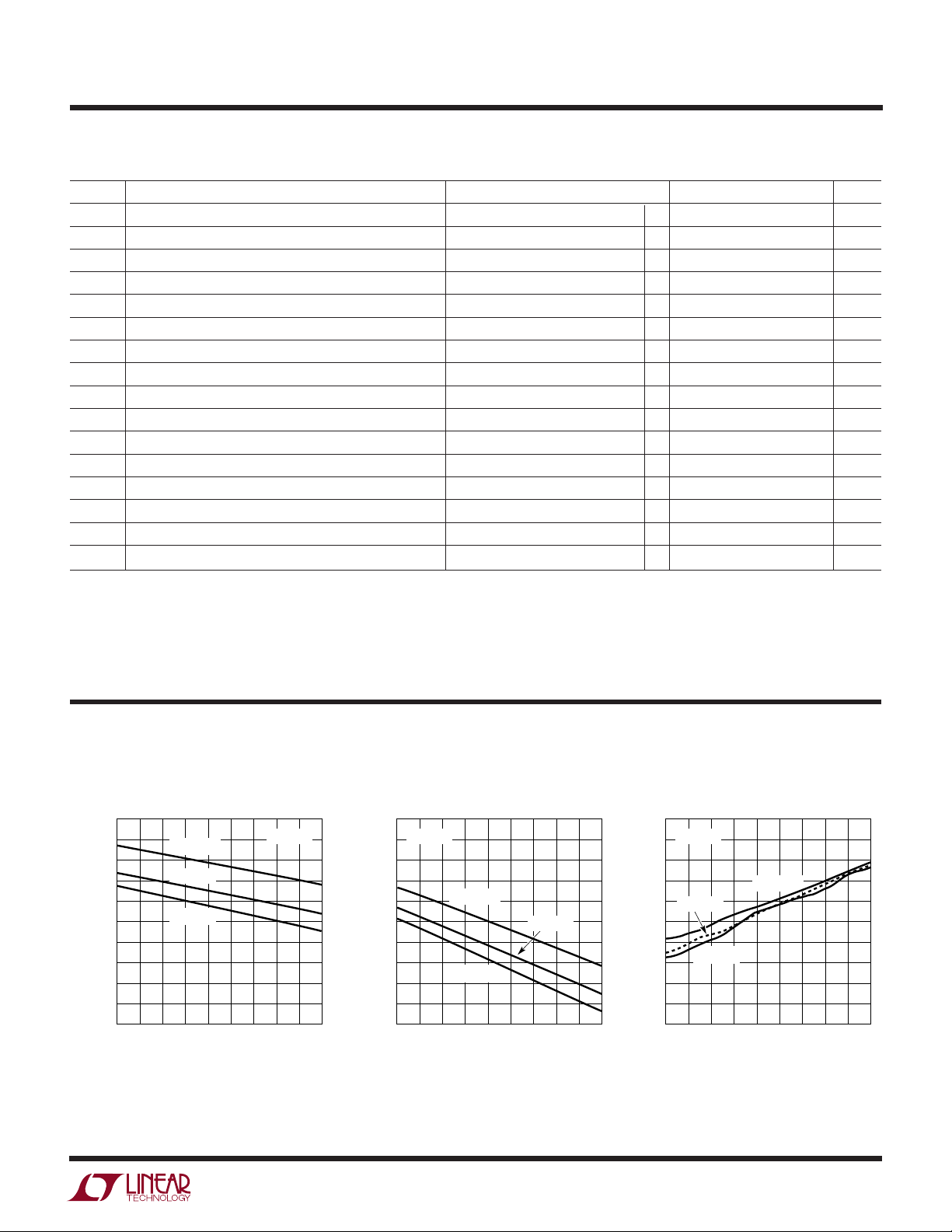
TYPICAL PERFOR A CE CHARACTERISTICS
Receiver Input Threshold Voltage
(Output High) vs Temperature
0
–20
–40
–60
–80
–100
–120
–140
–160
–180
RECEIVER INPUT THRESHOLD VOLTAGE (mV)
–200
–55 –35 –15 5 25 45 65 85 105 125
VCM = 12V
VCM = 0V
VCM = –7V
TEMPERATURE (°C)
VCC = 5V
1690 G01
Receiver Input Threshold Voltage
(Output Low) vs Temperature
0
VCC = 5V
–20
–40
–60
–80
–100
–120
–140
–160
–180
RECEIVER INPUT THRESHOLD VOLTAGE (mV)
–200
–55 –35 –15 5 25 45 65 85 105 125
VCM = 12V
VCM = 0V
VCM = –7V
TEMPERATURE (°C)
1690 G02
Receiver Hysteresis vs
Temperature
100
VCC = 5V
90
80
70
60
VCM = 0V
50
40
30
20
RECEIVER HYSTERESIS (mV)
10
VCM = –7V
0
–55 –35 –15 5 25 45 65 85 105 125
VCM = 12V
TEMPERATURE (°C)
1690 G03
3
Page 4
LTC1690
UW
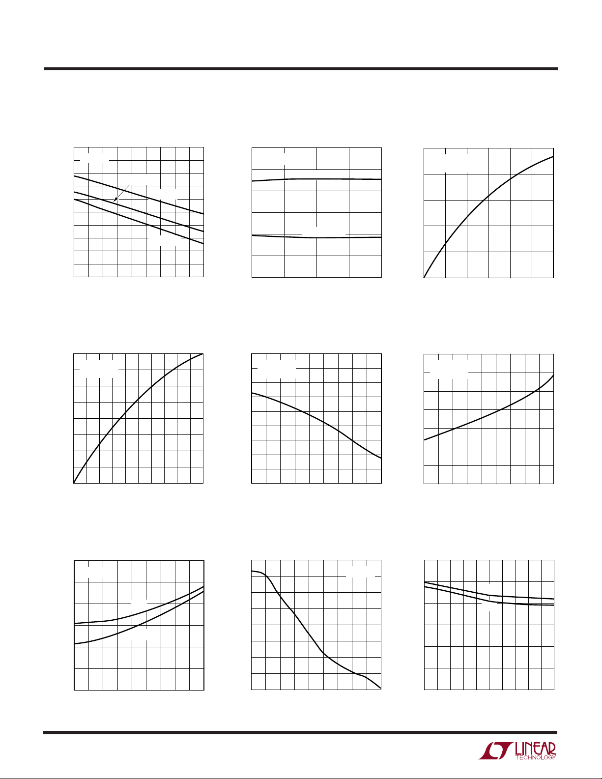
TYPICAL PERFOR A CE CHARACTERISTICS
Receiver Input Offset Voltage vs
Temperature
0
VCC = 5V
–20
–40
–60
–80
–100
–120
–140
–160
–180
RECEIVER INPUT OFFSET VOLTAGE (mV)
–200
–55 –35 –15 5 25 45 65 85 105 125
VCM = 0V
VCM = –7V
VCM = 12V
TEMPERATURE (°C)
Receiver Output Low Voltage vs
Output Current
40
TA = 25°C
35
= 4.75V
V
CC
30
25
20
15
10
RECEIVER OUTPUT CURRENT (mA)
5
0
0 0.2 0.4 0.6 0.8 1 1.2 1.4 1.6 1.8 2
RECEIVER OUTPUT LOW VOLTAGE (V)
1690 G04
1690 G07
Receiver Input Threshold Voltage
vs Supply Voltage
–40
TA = 25°C
–60
–80
–100
–120
–140
RECEIVER INPUT THRESHOLD VOLTAGE (mV)
–160
4.5 4.75 5 5.25 5.5
OUTPUT HIGH
OUTPUT LOW
SUPPLY VOLTAGE (V)
Receiver Output High Voltage vs
Temperature
4.8
I = 8mA
4.6
V
= 4.75V
CC
4.4
4.2
4.0
3.8
3.6
3.4
3.2
RECEIVER OUTPUT HIGH VOLTAGE (V)
3.0
–55 –35 –15 5 25 45 65 85 105 125
TEMPERATURE (°C)
1690 G05
1690 G08
Receiver Output High Voltage vs
Output Current
–25
TA = 25°C
V
= 4.75V
CC
–20
–15
–10
–5
RECEIVER OUTPUT CURRENT (mA)
0
4.5 4 3
5
RECEIVER OUTPUT HIGH VOLTAGE (V)
3.5
Receiver Output Low Voltage vs
Temperature
0.7
I = 8mA
= 4.75V
V
0.6
CC
0.5
0.4
0.3
0.2
0.1
RECEIVER OUTPUT LOW VOLTAGE (V)
0
–55 –35 –15 5 25 45 65 85 105 125
TEMPERATURE (°C)
2.5
2
1690 G06
1690 G09
Receiver Propagation Delay vs
Temperature
120
VCC = 5V
110
100
90
80
70
RECEIVER PROPAGATION DELAY (ns)
60
–55 –35 –15 5 25 45 65 85 105 125
t
PLH
t
PHL
TEMPERATURE (°C)
4
1690 G10
Receiver Skew t
PLH
– t
PHL
Temperature
10
9
8
7
6
5
RECEIVER SKEW (ns)
4
3
2
–55 –35 –15 5 25 45 65 85 105 125
TEMPERATURE (°C)
VCC = 5V
vs
1690 G11
Receiver Propagation Delay vs
Supply Voltage
110
100
90
80
70
60
RECEIVER PROPAGATION DELAY (ns)
50
4.5 4.6 4.7 4.8 4.9 5 5.1 5.2 5.3 5.4 5.5
t
PLH
t
PHL
SUPPLY VOLTAGE (V)
1690 G12
Page 5

UW
TYPICAL PERFOR A CE CHARACTERISTICS
LTC1690
Receiver Short-Circuit Current vs
Temperature Supply Current vs Temperature
70
60
50
40
30
20
SHORT-CIRCUIT CURRENT (mA)
10
0
–55 –35 –15 5 25 45 65 85 105 125
OUTPUT LOW
OUTPUT HIGH
TEMPERATURE (°C)
VCC = 5.25V
Driver Differential Output Voltage
vs Temperature
2.9
RL = 44Ω
2.7
2.5
2.3
2.1
1.9
1.7
DRIVER DIFFERENTIAL OUTPUT VOLTAGE (V)
1.5
VCC = 5.25V
VCC = 5V
VCC = 4.5V
VCC = 4.75V
–55 –35 –15 5 25 45 65 85 105 125
TEMPERATURE (°C)
1690 G13
1690 G16
340
320
300
280
260
240
220
200
180
SUPPLY CURRENT (µA)
160
140
120
–55 –35 –15 5 25 45 65 85 105 125
VCC = 5.25V
VCC = 4.75V
VCC = 5V
TEMPERATURE (°C)
Driver Differential Output Voltage
vs Temperature
2.9
2.7
2.5
2.3
2.1
1.9
1.7
DRIVER DIFFERENTIAL OUTPUT VOLTAGE (V)
1.5
VCC = 5.25V
VCC = 5V
VCC = 4.5V
VCC = 4.75V
–55 –35 –15 5 25 45 65 85 105 125
TEMPERATURE (°C)
1690 G14
RL = 54Ω
1690 G17
Logic Input Threshold Voltage vs
Temperature
1.75
1.70
1.65
1.60
1.55
LOGIC INPUT THRESHOLD VOLTAGE (V)
1.50
–55 –35 –15 5 25 45 65 85 105 125
VCC = 5.25V
VCC = 5V
VCC = 4.75V
TEMPERATURE (°C)
Driver Differential Output Voltage
vs Temperature
3.4
RL = 100Ω
3.2
3.0
2.8
2.6
2.4
DRIVER DIFFERENTIAL OUTPUT VOLTAGE (V)
2.2
–55 –35 –15 5 25 45 65 85 105 125
VCC = 5.25V
VCC = 5V
VCC = 4.75V
VCC = 4.5V
TEMPERATURE (°C)
1690 G15
1690 G18
Driver Common Mode Output
Voltage vs Temperature
3.0
2.5
VCC = 5.25V
2.0
1.5
1.0
0.5
RL = 44Ω
DRIVER COMMON MODE OUTPUT VOLTAGE (V)
0
–55 –35 –15 5 25 45 65 85 105 125
VCC = 5V
VCC = 4.75V
VCC = 4.5V
TEMPERATURE (°C)
1690 G19
Driver Common Mode Output
Voltage vs Temperature
3.0
2.5
VCC = 5.25V
2.0
1.5
1.0
0.5
RL = 54Ω
DRIVER COMMON MODE OUTPUT VOLTAGE (V)
0
–55 –35 –15 5 25 45 65 85 105 125
VCC = 5V
VCC = 4.75V
VCC = 4.5V
TEMPERATURE (°C)
1690 G20
Driver Common Mode Output
Voltage vs Temperature
3.0
2.5
VCC = 5.25V
2.0
1.5
1.0
0.5
RL = 100Ω
DRIVER COMMON MODE OUTPUT VOLTAGE (V)
0
–55 –35 –15 5 25 45 65 85 105 125
VCC = 5V
VCC = 4.75V
VCC = 4.5V
TEMPERATURE (°C)
1690 G21
5
Page 6

LTC1690
TEMPERATURE (°C)
–55 –35 –15 5 25 45 65 85 105 125
RECEIVER INPUT RESISTANCE (kΩ)
1690 G30
25
24
23
22
21
20
VCC = 5V
VCM = 12V
VCM = –7V
UW
TYPICAL PERFOR A CE CHARACTERISTICS
Driver Differential Output Voltage
vs Output Current
100
90
80
70
60
50
40
30
OUTPUT CURRENT (mA)
20
10
0
012345
DRIVER DIFFERENTIAL OUTPUT VOLTAGE (V)
TA = 25°C
1690 G22
Driver Output High Voltage vs
Output Current
–100
–80
–60
–40
OUTPUT CURRENT (mA)
–20
0
01234
DRIVER OUTPUT HIGH VOLTAGE (V)
Driver Propagation Delay vs
Temperature Driver Skew vs Temperature
30
VCC = 5V
25
20
t
t
PHL
PLH
4.0
VCC = 5V
3.5
3.0
TA = 25°C
= 5V
V
CC
1690 G23
Driver Output Low Voltage vs
Output Current
100
TA = 25°C
90
= 5V
V
CC
80
70
60
50
40
30
OUTPUT CURRENT (mA)
20
10
0
0.5 1 1.5 2 2.5 3
0
DRIVER OUTPUT LOW VOLTAGE (V)
Driver Propagation Delay vs
Supply Voltage
30
t
25
20
t
PHL
PLH
1690 G24
15
10
5
DRIVER PROPAGATION DELAY (ns)
0
4.6 4.7 4.8 4.9 5.0 5.1 5.2 5.3 5.4 5.5
4.5
SUPPLY VOLTAGE (V)
1690 G27
DRIVER SKEW (ns)
VCC = 5.25V
2.5
2.0
1.5
1.0
–55 –35 –15 5 25 45 65 85 105 125
1690 G29
TEMPERATURE (°C)
1690 G26
Receiver Input Resistance vs
Temperature
15
10
5
DRIVER PROPAGATION DELAY (ns)
0
–55 –35 –15 5 25 45 65 85 105 125
TEMPERATURE (°C)
1690 G25
Driver Short-Circuit Current vs
Temperature
250
200
OUTPUT HIGH
SHORT TO –7V
OUTPUT LOW
SHORT TO 10V
TEMPERATURE (°C)
DRIVER SHORT-CIRCUIT CURRENT (mA)
150
100
50
0
–55 –35 –15 5 25 45 65 85 105 125
6
Page 7

UUU
PIN FUNCTIONS
LTC1690
VCC (Pin 1): Positive Supply. 4.75V < VCC < 5.25V.
R (Pin 2): Receiver Output. R is high if (A – B) ≥ –10mV
and low if (A – B) ≤ –200mV.
D (Pin 3): Driver Input. If D is high, Y is taken high and Z
is taken low. If D is low, Y is taken low and Z is taken high.
GND (Pin 4): Ground.
TEST CIRCUITS
Y
R
V
OD2
R
V
Z
OC
1690 F01
Figure 1. Driver
DC Test Load #1
Y
V
OD3
Z
375Ω
60Ω
375Ω
V
TST
–7V TO 12V
1690 F02
Figure 2. Driver
DC Test Load #2
Y (Pin 5): Driver Output.
Z (Pin 6): Driver Output.
B (Pin 7): Receiver Input.
A (Pin 8): Receiver Input.
D
Y
R
DIFF
Z
Figure 3. Driver/Receiver
Timing Test Load
+
+
A
C
L1
R
C
L2
B
+
15pF
1690 F03
UWW
SWITCHI G TI E WAVEFOR S
3V
1.5V
D
0V
V
O
10%
–V
O
Z
V
O
Y
t
SKEW
50%
f = 1MHz, t
t
r
t
90%
PLH
1/2 V
≤ 10ns, t
r
V
= V(A) – V(B)
O
O
≤ 10ns
f
90%
1.5V
t
PHL
50%
10%
t
f
t
SKEW
1690 F04
Figure 4. Driver Propagation Delays
UU
FUNCTION TABLES
Driver
DZY
101
010
V
OD2
A – B
–V
R
OD2
V
5V
OL
0V
NOTE: t
SKD
Figure 5. Receiver Propagation Delays
Receiver
A – B R
≥ –0.01V 1
≤ –0.20V 0
Inputs Open 1
Inputs Shorted 1
= |t
f = 1MHz, t
t
PHL
1.5V
– t
PHL
PLH
|
≤ 10ns, t
r
INPUT
OUTPUT
≤ 10ns
f
0V
t
PLH
1.5V
1690 F05
Note: Table valid with or without termination resistors.
7
Page 8

LTC1690
U
WUU
APPLICATIONS INFORMATION
A typical application is shown in Figure 6. Two twisted pair
wires connect two driver/receiver pairs for full duplex data
transmission. Note that the driver and receiver outputs are
always enabled. If the outputs must be disabled, use the
LTC491. There are no restrictions on where the chips are
connected, and it isn’t necessary to have the chips connected to the ends of the wire. However, the wires must be
terminated at the ends with a resistor equal to their
characteristic impedance, typically 120Ω. Because only
one driver can be connected on the bus, the cable need
only be terminated at the receiving end. The optional
shields around the twisted pair are connected to GND at
one end and help reduce unwanted noise.
The LTC1690 can be used as a line repeater as shown in
Figure 7. If the cable is longer that 4000 feet, the LTC1690
is inserted in the middle of the cable with the receiver
output connected back to the driver input.
Receiver Fail-Safe
Some encoding schemes require that the output of the
receiver maintains a known state (usually a logic 1) when
data transmission ends and all drivers on the line are
forced into three-state. The receiver of the LTC1690 has a
fail-safe feature which guarantees the output to be in a
logic 1 state when the receiver inputs are left floating or
shorted together. This is achieved without external components by designing the trip-point of the LTC1690 to be
within –200mV to –10mV. If the receiver output must be
a logic 0 instead of a logic 1, external components are
required.
The LTC1690 fail-safe receiver is designed to reject fast
–7V to 12V common mode steps at its inputs. The slew
rate that the receiver will reject is typically 400V/µs, but
–7V to 12V steps in 10ns can be tolerated if the frequency
of the common mode step is moderate (<600kHz).
Driver-Receiver Crosstalk
The driver outputs generate fast rise and fall times. If the
LTC1690 receiver inputs are not terminated and floating,
switching noise from the LTC1690 driver can couple into
the receiver inputs and cause the receiver output to glitch.
This can be prevented by ensuring that the receiver inputs
are terminated with a 100Ω or 120Ω resistor, depending
on the type of cable used. A cable capacitance that is
greater than 10pF (≈1ft of cable) also prevents glitches if
no termination is present. The receiver inputs should not
be driven typically above 8MHz to prevent glitches.
8
5V
D
0.01µF
R
1
LTC1690
5
3
2
4
6
7
120Ω
8
Figure 6. Typical Application
SHIELD
120Ω
SHIELD
LTC1690
8
RECEIVER
7
6
5
1
2
3
4
1690 F06
5V
RDRIVER
0.01µF
DRECEIVER DRIVER
Page 9

LTC1690
U
WUU
APPLICATIONS INFORMATION
Fault Protection
When shorted to –7V or 10V at room temperature, the
short-circuit current in the driver outputs is limited by
internal resistance or protection circuitry to 250mA maximum. Over the industrial temperature range, the absolute
maximum positive voltage at any driver output should be
limited to 10V to avoid damage to the driver outputs. At
higher ambient temperatures, the rise in die temperature
due to the short-circuit current may trip the thermal
shutdown circuit.
The receiver inputs can withstand the entire –7V to 12V
RS485 common mode range without damage.
The LTC1690 includes a thermal shutdown circuit that
protects the part against prolonged shorts at the driver
outputs. If a driver output is shorted to another output or
to VCC, the current will be limited to a maximum of 250mA.
If the die temperature rises above 150°C, the thermal
shutdown circuit three-states the driver outputs to open
the current path. When the die cools down to about 130°C,
the driver outputs are taken out of three-state. If the short
persists, the part will heat again and the cycle will repeat.
This thermal oscillation occurs at about 10Hz and protects
the part from excessive power dissipation. The average
fault current drops as the driver cycles between active and
three-state. When the short is removed, the part will return
to normal operation.
If the outputs of two or more LTC1690 drivers are shorted
directly, the driver outputs cannot supply enough current
to activate the thermal shutdown. Thus, the thermal shutdown circuit will not prevent contention faults when two
drivers are active on the bus at the same time.
LTC1690
3
D DRIVER
2
R
RECEIVER
5
6
8
120Ω
7
Figure 7. Line Repeater
DATA
OUT
DATA
IN
1690 F07
9
Page 10

LTC1690
U
WUU
APPLICATIONS INFORMATION
Cables and Data Rate
The transmission line of choice for RS485 applications is
a twisted pair. There are coaxial cables (twinaxial) made
for this purpose that contain straight pairs, but these are
less flexible, more bulky and more costly than twisted
pairs. Many cable manufacturers offer a broad range of
120Ω cables designed for RS485 applications.
Losses in a transmission line are a complex combination
of DC conductor loss, AC losses (skin effect), leakage and
AC losses in the dielectric. In good polyethylene cables
such as Belden 9841, the conductor losses and dielectric
losses are of the same order of magnitude, leading to
relatively low overall loss (Figure 8).
When using low loss cable, Figure 9 can be used as a
guideline for choosing the maximum length for a given
data rate. With lower quality PVC cables, the dielectric loss
factor can be 1000 times worse. PVC twisted pairs have
terrible losses at high data rates (>100kbits/s), reducing
the maximum cable length. At low data rates, they are
acceptable and are more economical. The LTC1690 is
tested and guaranteed to drive CAT 5 cable and terminations as well as common low cost residential telephone
wire.
ESD PROTECTION
The ESD performance of the LTC1690 driver outputs (Z, Y)
and the receiver inputs (A, B) is as follows:
a) Meets ±15kV Human Body Model (100pF, 1.5kΩ).
b) Meets IEC1000-4-2 Level 4 (±8kV) contact mode speci-
fications.
c) Meets IEC1000-4-2 Level 3 (±8kV) air discharge speci-
fications.
This level of ESD performance means that external voltage
suppressors are not required in many applications, when
compared with parts that are only protected to ±2kV. The
LTC1690 driver input (D) and receiver output are protected to ±2kV per the Human Body Model.
When powered up, the LTC1690 does not latch up or
sustain damage when the Z, Y, A or B pins are subjected
to any of the conditions listed above. The data during the
ESD event may be corrupted, but after the event the
LTC1690 continues to operate normally.
The additional ESD protection at the LTC1690 Z, Y, A and
B pins is important in applications where these pins are
exposed to the external world via socket connections.
10
1.0
LOSS PER 100 FT (dB)
0.1
0.1
Figure 8. Attenuation vs Frequency for Belden 9841
1.0 10 100
FREQUENCY (MHz)
10
1690 F08
10k
1k
100
CABLE LENGTH (FT)
10
10k
Figure 9. RS485 Cable Length Recommended. Applies
for 24 Gauge, Polyethylene Dielectric Twisted Pair
100k 1M 10M
DATA RATE (bps)
2.5M
1690 F09
Page 11

PACKAGE DESCRIPTION
0.007
(0.18)
0.021
± 0.006
(0.53 ± 0.015)
* DIMENSION DOES NOT INCLUDE MOLD FLASH, PROTRUSIONS OR GATE BURRS. MOLD FLASH,
PROTRUSIONS OR GATE BURRS SHALL NOT EXCEED 0.006" (0.152mm) PER SIDE
** DIMENSION DOES NOT INCLUDE INTERLEAD FLASH OR PROTRUSIONS.
INTERLEAD FLASH OR PROTRUSIONS SHALL NOT EXCEED 0.006" (0.152mm) PER SIDE
° – 6° TYP
0
U
Dimensions in inches (millimeters) unless otherwise noted.
MS8 Package
8-Lead Plastic MSOP
(LTC DWG # 05-08-1660)
0.118 ± 0.004*
(3.00 ± 0.102)
0.193 ± 0.006
(4.90 ± 0.15)
SEATING
PLANE
0.040
± 0.006
(1.02 ± 0.15)
0.012
(0.30)
0.0256
REF
(0.65)
BSC
0.034 ± 0.004
(0.86 ± 0.102)
0.006 ± 0.004
(0.15 ± 0.102)
N8 Package
8-Lead PDIP (Narrow 0.300)
(LTC DWG # 05-08-1510)
8
7
12
LTC1690
6
5
0.118 ± 0.004**
(3.00 ± 0.102)
MSOP (MS8) 1098
4
3
0.300 – 0.325
(7.620 – 8.255)
0.065
(1.651)
0.009 – 0.015
(0.229 – 0.381)
+0.035
0.325
–0.015
+0.889
8.255
()
–0.381
*THESE DIMENSIONS DO NOT INCLUDE MOLD FLASH OR PROTRUSIONS.
MOLD FLASH OR PROTRUSIONS SHALL NOT EXCEED 0.010 INCH (0.254mm)
TYP
0.045 – 0.065
(1.143 – 1.651)
0.100
(2.54)
BSC
8-Lead Plastic Small Outline (Narrow 0.150)
0.010 – 0.020
(0.254 – 0.508)
0.008 – 0.010
(0.203 – 0.254)
*
DIMENSION DOES NOT INCLUDE MOLD FLASH. MOLD FLASH
SHALL NOT EXCEED 0.006" (0.152mm) PER SIDE
**
DIMENSION DOES NOT INCLUDE INTERLEAD FLASH. INTERLEAD
FLASH SHALL NOT EXCEED 0.010" (0.254mm) PER SIDE
× 45°
0.016 – 0.050
(0.406 – 1.270)
0.053 – 0.069
(1.346 – 1.752)
0°– 8° TYP
0.014 – 0.019
(0.355 – 0.483)
TYP
0.130 ± 0.005
(3.302 ± 0.127)
0.125
(3.175)
MIN
0.018 ± 0.003
(0.457 ± 0.076)
S8 Package
(LTC DWG # 05-08-1610)
0.004 – 0.010
(0.101 – 0.254)
0.050
(1.270)
BSC
0.020
(0.508)
MIN
0.228 – 0.244
(5.791 – 6.197)
0.255 ± 0.015*
(6.477 ± 0.381)
8
1
0.400*
(10.160)
MAX
876
12
0.189 – 0.197*
(4.801 – 5.004)
7
6
3
2
5
4
3
N8 1098
5
0.150 – 0.157**
(3.810 – 3.988)
4
SO8 1298
Information furnished by Linear Technology Corporation is believed to be accurate and reliable.
However, no responsibility is assumed for its use. Linear Technology Corporation makes no representation that the interconnection of its circuits as described herein will not infringe on existing patent rights.
11
Page 12

LTC1690
U
TYPICAL APPLICATIONS
Receiver with Low Fail-Safe Output
5V
1.2k
120Ω
1.2k
RECEIVER
RX
1690 TA02
RS232 IN
RS232 Receiver
2.7k
2.7k
RECEIVER
RX
1690 TA03
RELATED PARTS
PART NUMBER DESCRIPTION COMMENTS
LTC485 5V Low Power RS485 Interface Transceiver Low Power
LTC1480 3.3V Ultralow Power RS485 Transceiver with Shutdown Lower Supply Voltage
LTC1481 5V Ultralow Power RS485 Transceiver with Shutdown Lowest Power
LTC1482 5V Low Power RS485 Transceiver with Carrier Detect Output Low Power, High Output State when Inputs are Open,
Shorted or Terminated, ±15kV ESD Protection
LTC1483 5V Ultralow Power RS485 Low EMI Transceiver with Shutdown Low EMI, Lowest Power
LTC1484 5V Low Power RS485 Transceiver with Fail-Safe Receiver Circuit Low Power, High Output State when Inputs are Open,
Shorted or Terminated, ±15kV ESD Protection
LTC1485 5V RS485 Transceiver High Speed, 10Mbps
LTC1487 5V Ultralow Power RS485 with Low EMI, Shutdown and Highest Input Impedance, Low EMI, Lowest Power
High Input Impedance
LTC490 5V Differential Driver and Receiver Pair Low Power, Pin Compatible with LTC1690
LTC491 5V Low Power RS485 Full-Duplex Transceiver Low Power
LTC1535 Isolated RS485 Transceiver 2500V
LTC1685 52Mbps, RS485 Fail-Safe Transceiver Pin Compatible with LTC485
LTC1686/LTC1687 52Mbps, RS485 Fail-Safe Driver/Receiver Pin Compatible with LTC490/LTC491
LT1785/LT1791 ±60V Fault Protected RS485 Half-/Full-Duplex Transceiver ±15kV ESD Protection
Isolation, Full Duplex
RMS
12
Linear Technology Corporation
1630 McCarthy Blvd., Milpitas, CA 95035-7417
(408) 432-1900 ● FAX: (408) 434-0507
●
www.linear-tech.com
1690f LT/TP 0400 4K • PRINTED IN USA
LINEAR TE CHNOLOGY CORPORATION 1998
 Loading...