

Page 1
FEATURES
■
Ultrahigh Speed:
■
Guaranteed Propagation Delay: 8ns ±4ns
100Mbps
Over Temperature
■
50Mbps Operation with VDD = 3V
■
Low Channel-to-Channel Skew: 500ps Typ
■
Low t
■
■
PLH/tPHL
Hot SwapTM Capable
Driver Outputs Maintain High Impedance in
Skew: 500ps Typ
Three-State or with Power Off
■
Short-Circuit Protected: 3mA Typ Output Current
for an Indefinite Short
■
Thermal Shutdown Protected
■
Single 5V or 3V Supply
■
Pin Compatible with LTC486/LTC487
U
APPLICATIO S
■
High Speed RS485 Twisted-Pair Drivers
■
High Speed Backplane Drivers
■
Complementary Clock Drivers
■
STS-1/OC-1 Data Drivers
■
SCSI Drivers
LTC1688/LTC1689
100Mbps RS485
Hot Swapable Quad Drivers
U
DESCRIPTIO
The LTC®1688/LTC1689 are ultrahigh speed, differential
bus/line drivers that can operate at data rates up to
100Mbps. Propagation delay is guaranteed at 8ns ±4ns
over the full operating temperature range. These devices
operate over the full RS485 common mode range (–7V
to 12V), and also meet RS422 requirements.
The driver outputs are Hot Swap capable, maintaining
backplane data integrity during board insertion and
removal. The drivers feature three-state outputs, maintaining high impedance over the entire common mode range
(–7V to 12V). Outputs also remain high impedance during
power-up and with the power off. A short-circuit feature
detects bus contention and substantially reduces driver
output current. Thermal shutdown circuitry protects the
parts from excessive power dissipation.
The LTC1688 allows all four drivers to be enabled together,
while the LTC1689 allows two drivers at a time to be
enabled.
The LTC1688/LTC1689 operate from a single 5V or 3V
supply and draw only 9mA of supply current.
, LTC and LT are registered trademarks of Linear Technology Corporation.
Hot Swap is a trademark of Linear Technology Corporation.
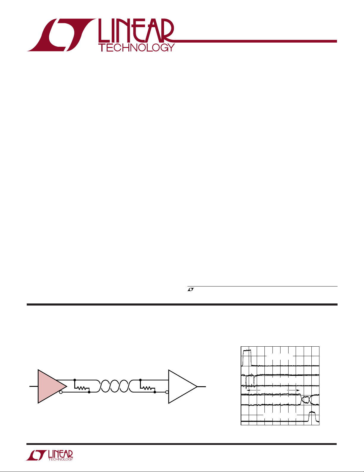
TYPICAL APPLICATIO
50Mbps RS485 Data Connection
DRIVER
100 FT CATEGORY 5 UTP
1/4 LTC1688
U
20ns Pulse Across 100 Feet
of Category 5 UTP
2V/DIV
100Ω100Ω
RECEIVER
1/4 LTC1518
1688/89 TA01
2V/DIV
2V/DIV
5V/DIV
DRIVER INPUT
DRIVER OUTPUTS
CABLE DELAY
RECEIVER INPUT
RECEIVER OUTPUT
20ns/DIV
1688/89 TA02
1
Page 2
LTC1688/LTC1689
A
W
O
LUTEXI TIS
S
A
WUW
U
ARB
G
PACKAGE
/
O
RDER I FOR ATIO
WU
(Note 1)
Supply Voltage (VDD)................................................ 7V
Enable Input Voltages................. –0.5V to (VDD + 0.5V)
Enable Input Currents..................... –100mA to 100mA
Driver Input Voltages.................. –0.5V to (VDD + 0.5V)
Driver Output Voltages ................. (–12V + VDD) to 12V
Driver Input Currents...................... –100mA to 100mA
Short-Circuit Duration (V
: –7V to 10V) ...... Indefinite
OUT
Operating Temperature Range.................... 0°C to 70°C
Storage Temperature Range................ –65°C to 150°C
Lead Temperature (Soldering, 10 sec)................. 300°C
DC ELECTRICAL CHARACTERISTICS
DI1
DO1A
DO1B
EN (EN12*)
DO2B
DO2A
DI2
GND
Consult factory for Industrial and Military grade parts.
The ● denotes the specifications which apply over the full operating
TOP VIEW
1
2
3
4
5
6
7
8
S PACKAGE
16-LEAD PLASTIC SO
*LTC1689 ONLY
T
= 150°C, θ
JMAX
JA
16
15
14
13
12
11
10
9
= 90°C/ W
V
DD
DI4
DO4A
DO4B
ENB (EN34*)
DO3B
DO3A
DI3
ORDER PART
NUMBER
LTC1688CS
LTC1689CS
temperature range, otherwise specifications are at TA = 25°C.
SYMBOL PARAMETER CONDITIONS MIN TYP MAX UNITS
VDD = 5V, Per Driver, TA = 25°C, Unless Otherwise Noted (Note 2)
V
OD1
V
OD2
∆V
OD
V
OC
∆VOC Change in Magnitude of Driver Common R = 25Ω or 50Ω, Figure 1 ● 0.2 V
V
IH
V
IL
I
IN1
I
OZ
I
DD
I
OSD1
I
OSD2
VDD = 3V, Per Driver, TA = 25°C, Unless Otherwise Noted (Note 2)
V
OD1
V
OD2
∆V
OD
V
OC
Differential Driver Output (Unloaded) I
Differential Driver Output (With Load) R = 50Ω (RS422) ● 2V
Change in Magnitude of Driver Differential R = 25Ω or 50Ω, Figure 1 ● 0.2 V
Output Voltage for Complementary
Output States
Driver Common Mode Output Voltage R = 25Ω or 50Ω, Figure 1 ● 23V
Mode Output Voltage for Complementary
Output States
Input High Voltage EN, ENB, EN12, EN34, DI ● 2V
Input Low Voltage EN, ENB, EN12, EN34, DI ● 0.8 V
Input Current EN, ENB, EN12, EN34, DI ● ±1 µA
Three-State (High Impedance) V
Output Current
Supply Current of Entire Device No Load, Digital Input Pins = 0V or V
Driver Short-Circuit Current, V
Driver Short-Circuit Current, V
Differential Driver Output (Unloaded) I
Differential Driver Output (With Load) R = 50Ω (RS422) 1.5 V
Change in Magnitude of Driver Differential R = 25Ω or 50Ω, Figure 1 0.1 V
Output Voltage for Complementary
Output States
Driver Common Mode Output Voltage R = 25Ω or 50Ω, Figure 1 1.3 V
= HIGH V
OUT
= LOW V
OUT
= 0 ● V
OUT
R = 25Ω (RS485), Figure 1
= –7V to 12V ● ±2 ±200 µA
OUT
DD
= –7V to 10V ● ±20 mA
OUT
= –7V to 10V ● ±20 mA
OUT
= 0 ● V
OUT
R = 25Ω (RS485), Figure 1
● 1.5 3.0 V
● 918 mA
● 0.65 2.0 V
DD
DD
U
V
V
2
Page 3
LTC1688/LTC1689
DC ELECTRICAL CHARACTERISTICS
The ● denotes the specifications which apply over the full operating
temperature range, otherwise specifications are at TA = 25°C.
SYMBOL PARAMETER CONDITIONS MIN TYP MAX UNITS
∆VOC Change in Magnitude of Driver Common R = 25Ω or 50Ω, Figure 1 0.1 V
Mode Output Voltage for Complementary
Output States
V
V
I
I
IH
IL
IN1
OZ
Input High Voltage EN, ENB, EN12, EN34, DI ● 1.4 V
Input Low Voltage EN, ENB, EN12, EN34, DI ● 0.5 V
Input Current EN, ENB, EN12, EN34, DI (Note 3) ● ±1 µA
Three-State (High Impedance) V
= –7V to 10V (Note 3) ● ±1 ±200 µA
OUT
Output Current
I
DD
I
OSD1
I
OSD2
Supply Current of Entire Device No Load, Digital Input Pins = 0V or V
Driver Short-Circuit Current, V
Driver Short-Circuit Current, V
= HIGH V
OUT
= LOW V
OUT
= –7V to 8V (Note 3) ● ±20 mA
OUT
= –7V to 8V (Note 3) ● ±20 mA
OUT
DD
5mA
U
SWITCHING CHARACTERISTICS
temperature range, otherwise specifications are at TA = 25°C.
SYMBOL PARAMETER CONDITIONS MIN TYP MAX UNITS
VDD = 5V, TA = 25°C, Unless Otherwise Noted (Note 2)
t
, t
PLH
t
SKEW
tr, t
t
ZH
t
ZL
t
LZ
t
HZ
C
L(MAX)
VDD = 3V, TA = 25°C, Unless Otherwise Noted (Note 2)
t
PLH
t
SKEW
tr, t
t
ZH
t
ZL
t
LZ
t
HZ
C
L(MAX)
Note 1: Absolute Maximum Ratings are those values beyond which the life
of a device may be impaired.
Driver Input-to-Output Propagation Delay R
PHL
Figures 2, 4
Driver Output-to-Output Skew R
Figures 2, 4
Driver Rise/Fall Time R
f
Figures 2, 4
Driver Enable to Output High CL = 25pF, S2 Closed, Figures 3, 5 ● 10 35 ns
Driver Enable to Output Low CL = 25pF, S1 Closed, Figures 3, 5 ● 10 35 ns
Driver Disable from Low CL = 15pF, S1 Closed, Figures 3, 5 ● 25 65 ns
Driver Disable from High CL = 15pF, S2 Closed, Figures 3, 5 ● 25 65 ns
Maximum Output Capacitive Load (Note 3) ● 200 pF
Maximum Data Rate (Note 3) ● 100 Mbps
Maximum Driver Input Rise/Fall Time (Note 3) ● 500 ns
, t
Driver Input-to-Output Propagation Delay R
PHL
Figures 2, 4
Driver Output-to-Output Skew R
Figures 2, 4
Driver Rise/Fall Time R
f
Figures 2, 4
Driver Enable to Output High CL = 25pF, S2 Closed, Figures 3, 5 25 ns
Driver Enable to Output Low CL = 25pF, S1 Closed, Figures 3, 5 25 ns
Driver Disable from Low CL = 15pF, S1 Closed, Figures 3, 5 50 ns
Driver Disable from High CL = 15pF, S2 Closed, Figures 3, 5 50 ns
Maximum Output Capacitive Load (Note 3) ● 200 pF
Maximum Data Rate 50 Mbps
Maximum Driver Input Rise/Fall Time (Note 3) ● 500 ns
The ● denotes the specifications which apply over the full operating
= 50Ω, CL1 = CL2 = 25pF, ● 4812 ns
DIFF
= 50Ω, CL1 = CL2 = 25pF, 500 ps
DIFF
= 50Ω, CL1 = CL2 = 25pF, 2 ns
DIFF
= 50Ω, CL1 = CL2 = 25pF, 11 ns
DIFF
= 50Ω, CL1 = CL2 = 25pF, 1 ns
DIFF
= 50Ω, CL1 = CL2 = 25pF, 4 ns
DIFF
Note 2: All currents into the device pins are positive; all currents out of the
device pins are negative.
Note 3: Guaranteed by design or correlation, but not tested.
3
Page 4
LTC1688/LTC1689
UW
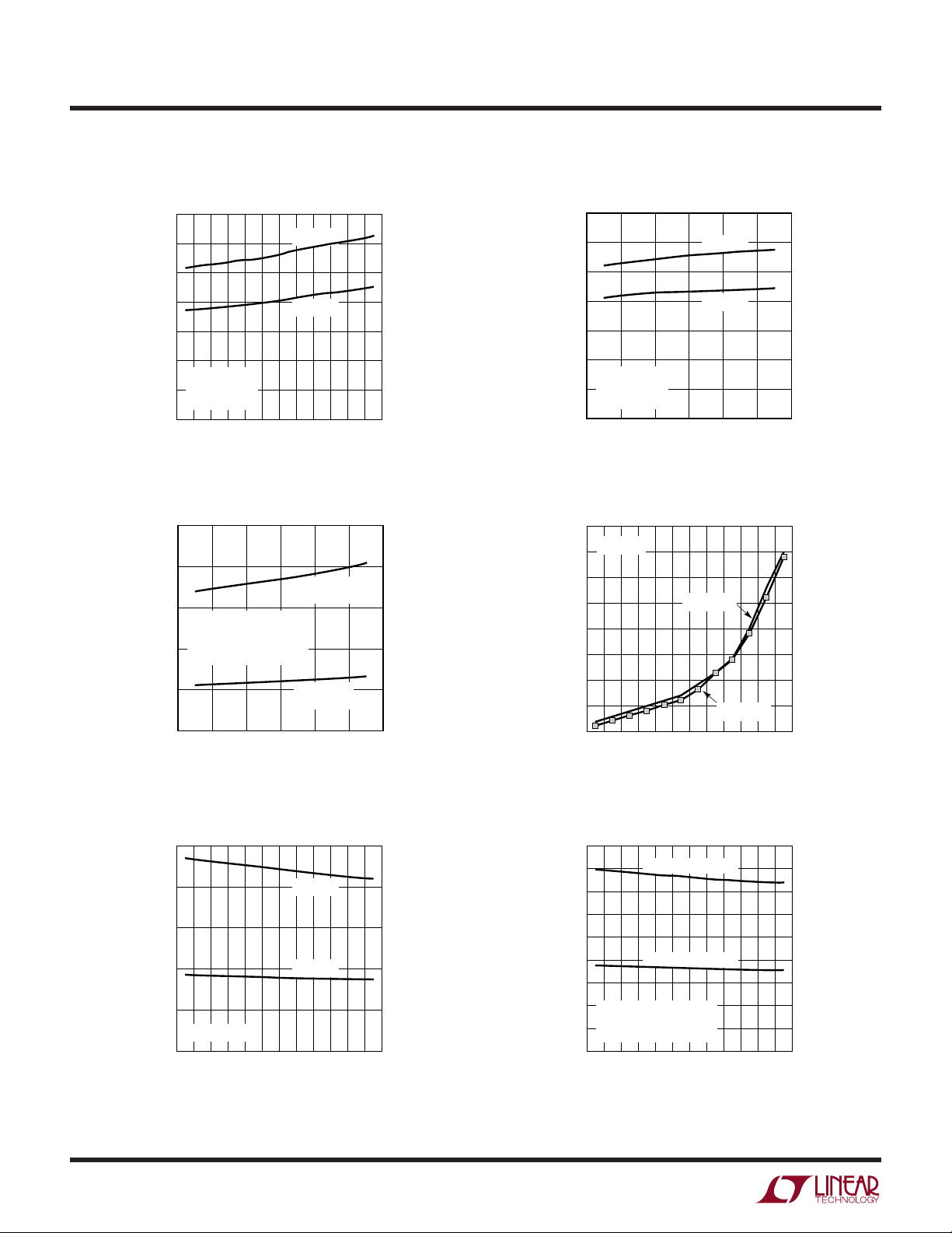
TYPICAL PERFORMANCE CHAR ACTERISTICS
Propagation Delay
vs Temperature
14
12
10
8
6
4
PROPAGATION DELAY (ns)
VDI = 0V TO 3V
= 50Ω
R
DIFF
2
= 25pF
C
L
0
0 20 40 60 80 100
TEMPERATURE (°C)
VDD = 3V
VDD = 5V
Supply Current vs Data Rate
250
200
4 DRIVERS
150
VDD = 5V
= 50Ω, PER DRIVER
R
DIFF
C
= 25pF, PER DRIVER
L
100
SUPPLY CURRENT (mA)
= 25°C
T
A
50
0
0 20 40 60 80 100 120
DATA RATE (Mbps)
SWITCHING
1 DRIVER
SWITCHING
1688/89 G01
1688/89 G03
Propagation Delay
vs Load Capacitance
14
12
10
8
6
4
PROPAGATION DELAY (ns)
VDI = 0V TO 3V
= 50Ω
R
DIFF
2
= 25°C
T
A
0
0 10 20 30 40 50 60
LOAD CAPACITANCE (pF)
VDD = 3V
VDD = 5V
Three-State Output Current
4.0
VDD = 5V
3.5
3.0
V
= –7V
2.5
2.0
1.5
OUTPUT CURRENT (µA)
1.0
0.5
0
0 20 40 60 80 100
OUT
V
TEMPERATURE (°C)
OUT
1688/89 G02
= 12V
1688/89 G04
4
vs Temperature
OD2
2.5
2.0
1.5
OD2
V
1.0
0.5
R
= 50Ω
DIFF
0
0 20 40 60 80 100
TEMPERATURE (°C)
VDD = 5V
VDD = 3V
1688/89 G05
IDD vs TemperatureV
180
160
140
120
100
(mA)
DD
I
80
60
40
20
0
4 DRIVERS LOADED
1 DRIVER LOADED
VDD = 5V
= 50Ω, PER DRIVER
R
DIFF
0.1Mbps
0 20 40 60 80 100
TEMPERATURE (°C)
1688/89 G06
Page 5

UUU
1688/89 TC03
OUTPUT
UNDER TEST
C
L
S1
500
DD
V
Ω
S2
PIN FUNCTIONS
LTC1688/LTC1689
DI1 (Pin 1): Driver 1 Input. Do not float.
DO1A (Pin 2): Driver 1 Noninverting Output.
DO1B (Pin 3): Driver 1 Inverting Output.
EN (Pin 4, LTC1688): High True Enable Pin, enables all
four drivers. A low on Pin 4 and a high on Pin 12 will put
all driver outputs into a high impedance state. See
Function Tables for details. Do not float.
EN12 (Pin 4, LTC1689): Enables Drivers 1 and 2. A low on
Pin 4 will put the outputs of drivers 1 and 2 into a high
impedance state. See Function Tables for details. Do not
float.
DO2B (Pin 5): Driver 2 Inverting Output.
DO2A (Pin 6): Driver 2 Noninverting Output.
DI2 (Pin 7): Driver 2 Input. Do not float.
GND (Pin 8): Ground Connection. A good ground plane is
recommended for all applications.
DI3 (Pin 9): Driver 3 Input. Do not float.
DO3A (Pin 10): Driver 3 Noninverting Output.
DO3B (Pin 11): Driver 3 Inverting Output.
ENB (Pin 12, LTC1688): Low True Enable Pin, enables all
four drivers. A low on Pin 4 and a high on Pin 12 will put
all driver outputs into a high impedance state. See
Function Tables for details. Do not float.
EN34 (Pin 12, LTC1689): Enables Drivers 3 and 4. A low
on Pin 12 will put the outputs of drivers 3 and 4 into a high
impedance state. See Function Tables for details. Do not
float.
DO4B (Pin 13): Driver 4 Inverting Output.
DO4A (Pin 14): Driver 4 Noninverting Output.
DI4 (Pin 15): Driver 4 Input. Do not float.
VDD (Pin 16): Power Supply Input. This pin should be
bypassed with a 0.1µF ceramic capacitor as close to the
pin as possible. Recommended: VDD = 3V to 5.25V.
U
U
FU CTIO TA B LES
LTC1688
INPUTS OUTPUTS
DI EN ENB OUTA OUTB
HH X H L
LHX L H
HX L H L
LX L L H
X L H HI-Z HI-Z
TEST CIRCUITS
A
R
V
OD
R
V
1688/89 TC01
OC
B
Figure 1. Driver DC Test Load
EN (EN12)
DI
DRIVER
ENB (EN34)
Figure 2. Driver Timing Test Circuit
A
B
LTC1689
R
DIFF
INPUTS OUTPUTS
DI EN12/EN34 OUTA OUTB
HHHL
LHLH
X L HI-Z HI-Z
C
L1
C
L2
1688/89 TC02
Figure 3. Driver Timing Test Load
5
Page 6

LTC1688/LTC1689
UW W
SWITCHI G TI E WAVEFOR S
3V
DI
0V
B
V
O
A
V
O
–V
O
1/2 V
1.5V
t
PLH
t
O
10%
t
r
SKEW
90%
Figure 4. Driver Propagation Delays
3V
EN
A, B
A, B
0V
5V
V
OL
V
OH
0V
1.5V 1.5V
t
ZL
1/2 V
DD
1/2 V
DD
t
ZH
Figure 5. Driver Enable and Disable Times
U
WUU
APPLICATIONS INFORMATION
f = 1MHz; tr < 3ns; tf < 3ns
V
= V(A) – V(B)
DIFF
f = 1MHz; t
≤ 3ns; tf ≤ 3ns
r
OUTPUT NORMALLY LOW
OUTPUT NORMALLY HIGH
1/2 V
1.5V
t
PHL
O
t
SKEW
90%
10%
t
f
t
LZ
0.5V
0.5V
t
HZ
1688/89 F04
1688/89 F05
The LTC1688/LTC1689 family of RS485 quad differential
drivers employs a novel architecture and fabrication process that allows ultra high speed operation (100Mbps)
and Hot Swap capability while maintaining the ruggedness
of RS485 operation (three-state outputs can float from
–7V to 12V with a single 5V supply). Unlike typical CMOS
drivers whose propagation delay can vary as much as
500%, the propagation delay of the LTC1688/LTC1689
drivers will only vary by ±50% (a narrow ±4ns window).
This performance is achieved by designing the input stage
of each driver to have minimum propagation delay shift
over temperature and from part to part.
The LTC1688/LTC1689 have an ESD rating of 6kV human
body model.
50Mbps with 3V Operation
The LTC1688/LTC1689 are designed to operate with a 3V
power supply and still achieve 50Mbps operation (see
Electrical Characteristics table for 3V DC and AC specifica-
tions). Figure 6 shows waveforms of an LTC1689 driving
a receiver using 100 feet of Category 5 UTP. Both parts are
operating at 3V supply.
LTC1689 OUTPUT
2V/DIV
FAR END OF CABLE
2V/DIV
RECEIVER OUTPUT
5V/DIV
20ns/DIV
1688/89 F06
Figure 6. 3V High Speed Data Transmission
6
Page 7

LTC1688/LTC1689
U
WUU
APPLICATIONS INFORMATION
Hot Swap Capability
With the LTC1688/LTC1689 outputs disabled but connected to the transmission line, the user can turn on/off the
power to the LTC1688/LTC1689 without inducing a differential signal on the transmission line. Due to capacitive
coupling, however, there can be a small amount of common mode charge injected into both disabled outputs,
which is not seen as a differential signal (see Figure 7). The
disabled outputs can be hooked/unhooked to a transmission line without disturbing the existing data.
Output Short-Circuit Protection
In addition to 100Mbps operation and Hot Swap capability,
the LTC1688/LTC1689 employ voltage sensing shortcircuit protection that reduces short-circuit current by
over an order of magnitude. For a given input polarity, this
circuitry determines what the correct output level should
be. If the output level is different from the expected, the
circuitry shuts off the big output devices. Much smaller
devices are instead turned on, thus producing a much
smaller short-circuit output current (3mA typical). For
example, if the driver input is >2V, it expects the “A” output
to be >3.25V and the “B” output to be less than 1.75V. If
the “A” output is subsequently shorted to a voltage below
VDD/2, this circuitry shuts off the big outputs and turns on
3mA current sources instead (the converse applies to the
“B” output). Note that these 3mA current sources are
active only during a short-circuit fault. During normal
operation, the regular output drivers can sink/source
>50mA.
A time-out period of about 50ns is required before a shortcircuit fault is detected. This circuitry might falsely detect
a short under excess output capacitive load (> 200pF).
Additionally, a short might go undetected if there is too
much resistance (user inserted or cable parasitic) between
the physical short and the actual driver output.
For cables with the recommended RS485 termination (no
DC bias on the cable, see Figure 8), the LTC1688/LTC1689
will automatically come out of short-circuit mode once the
physical short has been removed.
To prevent permanent damage to the part, the maximum
allowable short is 10V (not 12V). Note that during a short,
the voltage right at the pin should not ring to a voltage
higher than 12V. Instability could surface if the short is
made with long leads (parasitic inductance). Once the
short is removed, the instability will disappear.
A OUTPUT
B OUTPUT
Figure 7. Common Mode Charge Injection During Hot Swapping
7
Page 8

LTC1688/LTC1689
U
WUU
APPLICATIONS INFORMA TION
Cable Termination
The recommended cable termination for use with the
LTC1688/LTC1689 is a single resistor across the two ends
of a transmission cable (see Figure 8). When PC traces are
used as the transmission line, its characteristic impedance should be chosen close to 100Ω in order to better
match the specified timing characteristics of the LTC1688/
LTC1689. Category 5 unshielded twisted pair can be used
over short distances at the maximum data rates (100Mbps).
For point-to-point configurations (see Figure 9), a single
resistor across the cable at the receiver end is sufficient.
A single resistor termination lowers power consumption
and increases the differential output signal. See Enable
Pins section for cable terminations with a DC bias.
Enable Pins
For cable terminations with a DC bias (such as High
Voltage Differential SCSI, see Figure 10), the driver outputs must be disabled for at least 200ns after power-up.
This ensures that the driver outputs do not disturb the
cable upon power-up. It also ensures the correct output
start-up conditions. When there is an output short fault
condition and the cable has a DC biased termination, such
as Figure 10, the driver outputs must be disabled for at
least 200ns after the short has been removed. Recall that
for transmission lines that have the recommended RS485
single resistor termination (Figures 8 and 9), the LTC1688/
LTC1689 will come out of a short-circuit fault condition
automatically without having to disable the outputs.
1/4 LTC1688
1/4 LTC1519
100Ω 100Ω
Figure 8. Multipoint Transmission Figure 9. Point-to-Point Transmission
DE
1/4 LTC1688
DI
1/4 LTC1518
TERM POWER
330Ω
150Ω
330Ω
1688/89 F08
TERM POWER
1/4 LTC1518
1/4 LTC1689
330Ω
150Ω
330Ω
1/4 LTC1518
1688/89 F10
100Ω
1/4 LTC1518
1688/89 F09
8
Figure 10. DC-Biased Termination
(Recommended for SCSI Applications Only)
Page 9

LTC1688/LTC1689
U
WUU
APPLICATIONS INFORMATION
High Speed Twisted-Pair Transmission
Data rates up to 100Mbps can be transmitted over short
distances using Category 5 UTP (unshielded twisted pair).
The cable distance will determine the maximum data rate.
Figures 11 and 12 show an 8ns pulse propagating over 25
feet of Category 5 UTP. Notice how the cable attenuates the
signal. Lucent Technologies’ BRF2A and BRS2A receivers
are recommended for these ultrahigh speed applications.
2V/DIV
DRIVER INPUT
High Speed Backplane Transmission
The LTC1688/LTC1689 can be used in backplane point-topoint and multipoint applications. At high data rates,
signals should be routed differentially and PC traces
should be terminated (see Figure 13). Note that the RS485
specification calls for characteristic impedances near 100Ω;
therefore, PC trace transmission lines should be designed
with an impedance close to 100Ω. If trace impedance is
much less than 100Ω, and the trace is double terminated,
the part will experience excess heating. The propagation
delay could then fall outside the specified window. The
LT1720 dual UltraFastTM comparator is a good choice for
high data rate backplane applications.
2V/DIV
2V/DIV
5V/DIV
Figure 11. 8ns Pulse Over 25 Feet Category 5 UTP
DRIVER OUTPUT
RECEIVER INPUT
RECEIVER OUTPUT
10ns/DIV
1688/89 F11
1/4 LTC1688
DRIVER
Figure 13. 100Mbps Backplane Transmission
TRANSMISSION LINE
BACKPLANE
DRIVER
25 FT CATEGORY 5 UTP
1/4 LTC1688
Figure 12. 100Mbps Differential Data Connection
1/2 LT1720
100Ω
RECEIVER
1688/89 F13
100Ω100Ω
+
RECEIVER
–
1688/89 F12
UltraFast is a trademark of Linear Technology Corporation.
9
Page 10

LTC1688/LTC1689
U
WUU
APPLICATIONS INFORMA TION
Layout Considerations
A ground plane is recommended when using high frequency devices like the LTC1688/LTC1689. A 0.1µF
ceramic bypass capacitor less than 0.25 inch away from
the VDD pin is also recommended. Special care should be
taken to route the differential outputs very symmetrically
in order to obtain the same parasitic capacitances and thus
maintain good propagation delay skew.
Parasitic capacitance from each input to its corresponding
outputs should also be minimized. Any excess capacitance could result in slower operation or even instability.
Channel output pairs should be kept away from other
output pairs to avoid parasitic coupling.
Data Rate vs Cable Length
Cable length and quality limit the maximum data rate in a
twisted pair system. Category 5 unshielded twisted pair is
a good choice for high speed data transmission, as it
exhibits superior bandwidth over other cables of similar
cost.
Driver and receiver bandwidth affects the maximum data
rate only over distances of less than 100', even for the best
cables. The LTC1688/LTC1689 RS485 drivers and
LTC1518/LTC1519 52Mbps RS485 receivers are the fastest in the industry. The LTC1688/LTC1689 drivers can
reach speeds over 100Mbps, with a rise and fall time of
just 2ns. At speeds in excess of 52Mbps, the non-RS485
Lucent Technologies’ BRF2A receiver is recommended.
Detailed information on data rate vs cable length is provided by the cable manufacturer. They characterize their
cables for bit rate and 0% to 50% rise time vs cable length,
allowing a rapid comparison of various cable types.
The following oscilloscope waveforms illustrate how a
cable attenuates the signal and slows its rise time at
different lengths. Also shown are the driver input and
receiver output.
DRIVER
1/4 LTC1688
1/4 LTC1689
CATEGORY 5 CABLE
UNDER TEST
100Ω100Ω
Figure 14. Test Circuit for Cable Speed Evaluation
CABLE DELAY
2V/DIV
2µs/DIV
RECEIVER
DRIVER INPUT
RECEIVER INPUT
RECEIVER OUTPUT
1688/89 F16
1688/89 F14
CABLE DELAY
2V/DIV
2µs/DIV
Figure 15. 4000 Feet, 0.5Mbps, LTC1518 Receiver
CABLE DELAY
2V/DIV
500ns/DIV
DRIVER INPUT
RECEIVER INPUT
RECEIVER OUTPUT
1688/89 F15
DRIVER INPUT
RECEIVER INPUT
RECEIVER OUTPUT
1688/89 F17
10
Figure 17. 1000 Feet, 2Mbps, LTC1518 ReceiverFigure 16. 4000 Feet, 1Mbps, LTC1518 Receiver
Page 11

LTC1688/LTC1689
U
WUU
APPLICATIONS INFORMATION
DRIVER INPUT
CABLE DELAY
2V/DIV
500ns/DIV
RECEIVER INPUT
RECEIVER OUTPUT
1688/89 F18
2V/DIV
CABLE DELAY
Figure 19. 1000 Feet, 1Mbps, LTC1518 ReceiverFigure 18. 1000 Feet, 5Mbps, LTC1518 Receiver
1µs/DIV
DRIVER INPUT
RECEIVER INPUT
RECEIVER OUTPUT
1688/89 F19
2V/DIV
2V/DIV
CABLE DELAY
CABLE DELAY
100ns/DIV
DRIVER INPUT
RECEIVER INPUT
RECEIVER OUTPUT
1688/89 F20
DRIVER INPUT
RECEIVER INPUT
2V/DIV
2V/DIV
DRIVER INPUT
CABLE DELAY
50ns/DIV
RECEIVER INPUT
RECEIVER
OUTPUT
1688/89 F21
Figure 21. 200 Feet, 33Mbps, LTC1518 ReceiverFigure 20. 200 Feet, 20Mbps, LTC1518 Receiver
DRIVER INPUT
CABLE DELAY
RECEIVER INPUT
RECEIVER OUTPUT
50ns/DIV
1688/89 F22
Figure 23. 25 Feet, 100Mbps, BRF2A ReceiverFigure 22. 100 Feet, 50Mbps, LTC1518 Receiver
Information furnished by Linear Technology Corporation is believed to be accurate and reliable.
However, no responsibility is assumed for its use. Linear Technology Corporation makes no representation that the interconnection of its circuits as described herein will not infringe on existing patent rights.
10ns/DIV
RECEIVER
OUTPUT
11
1688/89 F23
Page 12

LTC1688/LTC1689
PACKAGE DESCRIPTION
U
Dimensions in inches (millimeters) unless otherwise noted.
S Package
16-Lead Plastic Small Outline (Narrow 0.150)
(LTC DWG # 05-08-1610)
0.386 – 0.394*
(9.804 – 10.008)
13
16
14
15
12
11
10
9
0.010 – 0.020
(0.254 – 0.508)
0.008 – 0.010
(0.203 – 0.254)
*
DIMENSION DOES NOT INCLUDE MOLD FLASH. MOLD FLASH
SHALL NOT EXCEED 0.006" (0.152mm) PER SIDE
**
DIMENSION DOES NOT INCLUDE INTERLEAD FLASH. INTERLEAD
FLASH SHALL NOT EXCEED 0.010" (0.254mm) PER SIDE
×
°
45
0.016 – 0.050
(0.406 – 1.270)
0° – 8° TYP
0.228 – 0.244
(5.791 – 6.197)
0.053 – 0.069
(1.346 – 1.752)
0.014 – 0.019
(0.355 – 0.483)
TYP
0.150 – 0.157**
(3.810 – 3.988)
4
5
0.050
(1.270)
BSC
3
2
1
7
6
8
0.004 – 0.010
(0.101 – 0.254)
S16 1098
RELATED PARTS
PART NUMBER DESCRIPTION COMMENTS
LTC486/LTC487 Low Power Quad RS485 Drivers 110µA Typ Supply Current, 10Mbps, –7V to 12V Common Mode Range
LT®1394 7ns UltraFast Single Supply Comparator 6mA Typ Supply Current, Ground Sensing on Single Supply
LTC1518/LTC1519 High Speed, Precision Quad RS485 Receivers 52Mbps, Pin Compatible with LTC488/LTC489
LTC1520 High Speed, Precision Quad Differential Line Receiver Single Supply, 18ns Propagation Delay, 100mV Threshold
LTC1685 High Speed, Precision RS485 Transceiver 52Mbps, Pin Compatible with LTC485
LTC1686/LTC1687 High Speed, Precision RS485 Full-Duplex Transceivers 52Mbps, Pin Compatible with LTC490/LTC491
LT1720 Dual 4.5ns UltraFast Single Supply Comparator 4mA per Comparator, Optimized for 3V or 5V Operation
16889f LT/TP 1099 4K • PRINTED IN THE USA
LINEAR TECHNOLOGY CORPORATION 1999
12
Linear Technology Corporation
1630 McCarthy Blvd., Milpitas, CA 95035-7417
(408) 432-1900 ● FAX: (408) 434-0507
●
www.linear-tech.com
 Loading...