

Page 1
FEATURES
■
Precision Propagation Delay Over Temperature:
Receiver/Driver: 18.5ns ±3.5ns
■
High Data Rate:
■
Low t
PLH/tPHL
52Mbps
Skew:
Receiver/Driver: 500ps Typ
■
–7V to 12V RS485 Input Common Mode Range
■
Guaranteed Fail-Safe Operation Over the Entire
Common Mode Range
■
High Input Resistance: ≥22k, Even When Unpowered
■
Short-Circuit Protected
■
Thermal Shutdown Protected
■
Driver Maintains High Impedance in Three-State or
with Power Off
■
Single 5V Supply
■
Pin Compatible with LTC490/LTC491
■
45dB CMRR at 26MHz
U
APPLICATIONS
■
High Speed RS485/RS422 Full Duplex Transceivers
■
Level Translator
■
Backplane Transceiver
■
STS-1/OC-1 Data Transceiver
■
Signal Repeaters
LTC1686/LTC1687
52Mbps Precision Delay
RS485 Fail-Safe Transceivers
U
DESCRIPTION
The LTC®1686/LTC1687 are high speed, precision delay,
full-duplex RS485 transceivers that can operate at data
rates as high as 52Mbps. The devices also meet the
requirements of RS422.
A unique architecture provides very stable propagation
delays and low skew over a wide common mode and
ambient temperature range.
The driver and receiver feature three-state outputs, with
disabled driver outputs maintaining high impedance over
the entire common mode range. A short-circuit feature
detects shorted outputs and substantially reduces driver
output current. A similar feature also protects the receiver
output from short circuits. Thermal shutdown circuitry
protects from excessive power dissipation.
The receiver has a fail-safe feature that guarantees a high
output state when the inputs are shorted or are left floating.
The LTC1686/LTC1687 RS485 transceivers guarantee
receiver fail-safe operation over the
range (–7V to 12V). Receiver input resistance remains
≥ 22k when the device is unpowered or disabled.
The LTC1686/LTC1687 operate from a single 5V supply
and draw only 7mA of supply current.
, LTC and LT are registered trademarks of Linear Technology Corporation.
entire
common mode
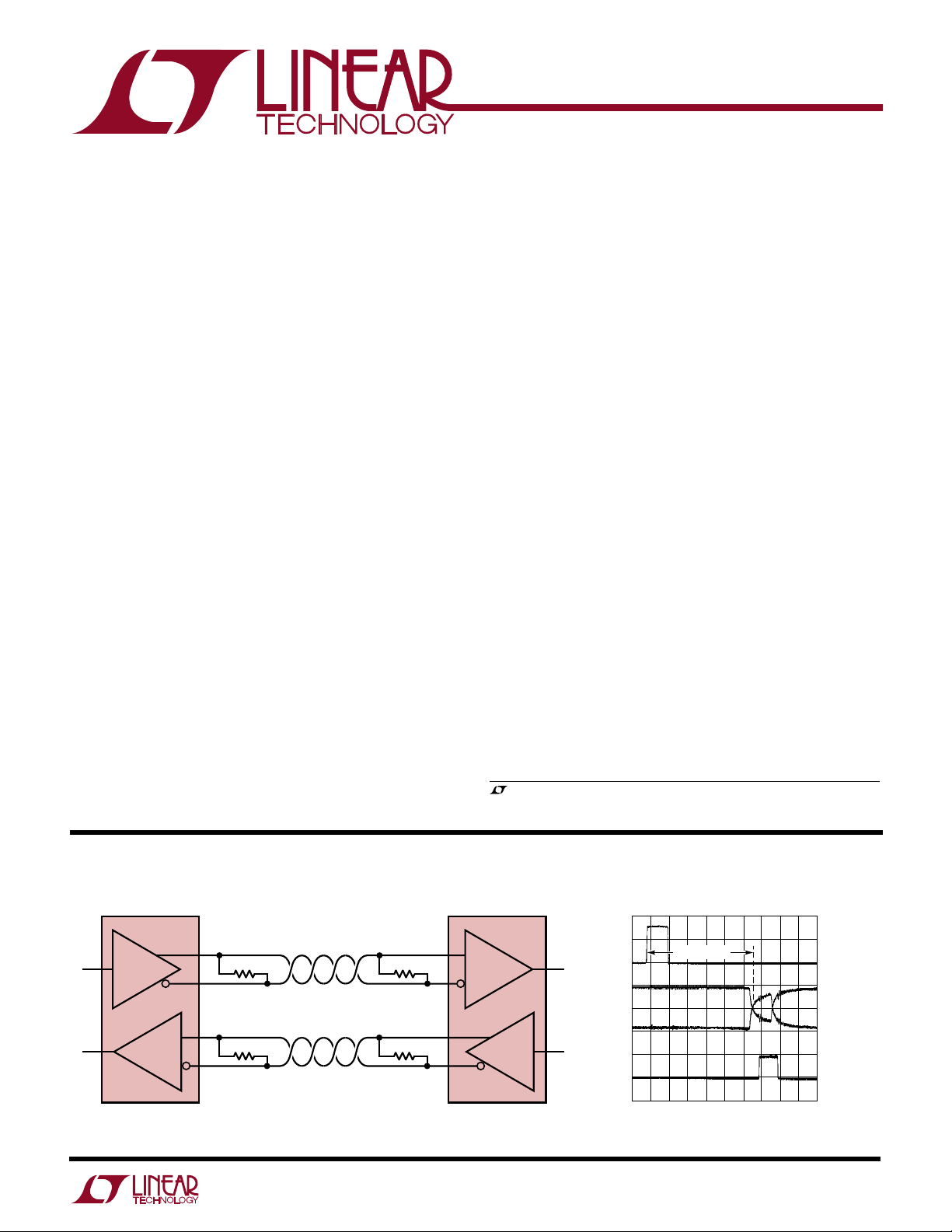
TYPICAL APPLICATION
LTC1686 LTC1686
3
D
R
DRIVER
2
RECEIVER
5
100Ω 100Ω
6
8
100Ω 100Ω
7
400 FT OF CATEGORY 5 UTP
U
RECEIVER
DRIVER
LTC1686/87 • TA01
10Mbps Data Pulse
400 Feet Category 5 UTP
1686/87 TA02
DRIVER INPUT
RECEIVER
INPUT
RECEIVER
OUTPUT
2V/DIV
R
1V/DIV
D
5V/DIV
CABLE DELAY
100ns/DIV
1
Page 2
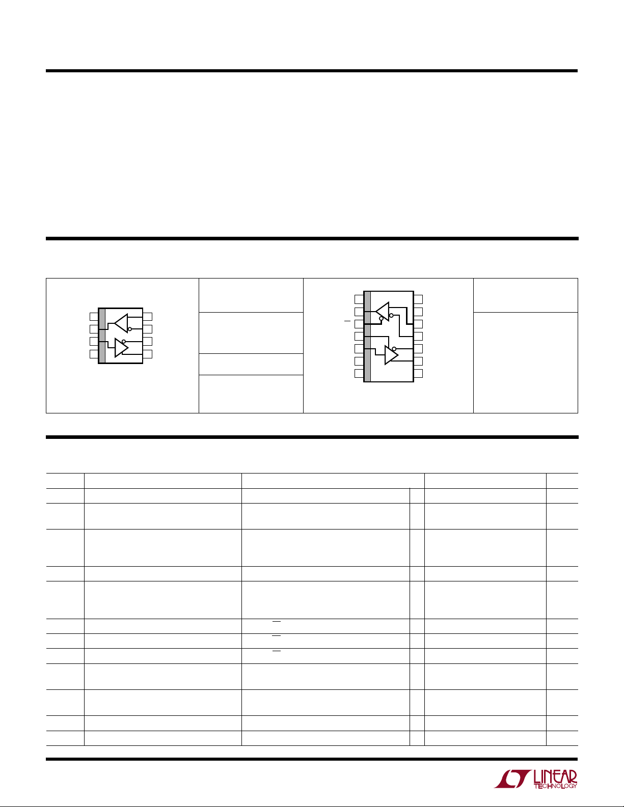
LTC1686/LTC1687
S8 PACKAGE
8-LEAD PLASTIC SO
1
2
3
4
8
7
6
5
TOP VIEW
V
DD
R
D
GND
A
B
Z
Y
R
D
A
W
O
LUTEXI T
S
A
WUW
ARB
U
G
I
S
(Note 1)
Supply Voltage (VDD).............................................. 10V
Control Input Currents .................... –100mA to 100mA
Control Input Voltages .................. –0.5V to VDD + 0.5V
Driver Input Voltages .................... –0.5V to VDD + 0.5V
Driver Output Voltages ................................. +12V/– 7V
Receiver Input Voltages ................................ +12V/–7V
Receiver Output Voltages ............. –0.5V to VDD + 0.5V
Receiver Input Differential ...................................... 10V
PACKAGE
/
O
RDER I FOR ATIO
WU
U
ORDER PART
NUMBER
LTC1686CS8
S8 PART MARKING
T
= 125°C, θ
JMAX
Consult factory for Industrial and Military grade parts.
= 150°C/ W
JA
1686
Driver Short-Circuit Duration
(V
: –7V to 10V)...................................... Indefinite
OUT
Receiver Short-Circuit Duration
(V
: 0V to VDD) ........................................ Indefinite
OUT
Operating Temperature Range .................... 0°C to 70°C
Storage Temperature Range ................ –65°C to 150°C
Lead Temperature (Soldering, 10 sec)................. 300°C
1
NC
2
R
3
RE
4
DE
5
D
6
GND
GND
14-LEAD PLASTIC SO
T
JMAX
TOP VIEW
R
S PACKAGE
= 125°C, θ
D
JA
14
13
12
11
10
9
87
= 90°C/W
V
DD
NC
A
B
Z
Y
NC
ORDER PART
NUMBER
LTC1687CS
DC ELECTRICAL CHARACTERISTICS
SYMBOL PARAMETER CONDITIONS MIN TYP MAX UNITS
V
OD1
V
OD2
∆V
OD
V
OC
∆VOC Change in Magnitude of Driver Common R = 27Ω or 50Ω, Figure 1 ● 0.2 V
V
IH
V
IL
I
IN1
I
IN2
V
TH
∆V
TH
V
OH
2
Differential Driver Output (Unloaded) I
Differential Driver Output (With Load) R = 50Ω (RS422) 2.0 V
Change in Magnitude of Driver Differential R = 27Ω or 50Ω, Figure 1 ● 0.2 V
Output Voltage for Complementary
Output States
Driver Common Mode Output Voltage R = 27Ω or 50Ω, VDD = 5V, Figure 1 ● 23V
Mode Output Voltage for Complementary
Output States
Input High Voltage D, DE, RE ● 2V
Input Low Voltage D, DE, RE ● 0.8 V
Input Current D, DE, RE ● –1 1 µA
Input Current (A, B) VA, VB = 12V, VDD = 0V or 5.25V ● 500 µA
Differential Input Threshold Voltage –7V ≤ VCM ≤ 12V ● –0.3 0.3 V
for Receiver
Receiver Input Hysteresis VCM = 0V 25 mV
Receiver Output High Voltage I
= 0 ● V
OUT
R = 27Ω (RS485), Figure 1 ● 1.5 V
, VB = –7V, VDD = 0V or 5.25V ● –500 µA
V
A
= –4mA, VID = 300mV ● 3.5 4.8 V
OUT
VDD = 5V ± 5% unless otherwise noted (Notes 2, 3).
DD
DD
V
V
Page 3
LTC1686/LTC1687
DC ELECTRICAL CHARACTERISTICS
VDD = 5V ±5% unless otherwise noted (Notes 2, 3).
SYMBOL PARAMETER CONDITIONS MIN TYP MAX UNITS
V
I
OL
OZR
Receiver Output Low Voltage I
= 4mA, VID = –300mV ● 0.4 V
OUT
Three-State (High Impedance) Output 0.4V ≤ V
≤ 2.4V ● –1 1 µA
OUT
Current at Receiver
I
OZD
Three-State (High Impedance) Output V
= –7V to 12V ● –200 200 µA
OUT
Current at Driver
C
LOAD
I
DD
I
OSD1
I
OSD2
I
OSR
R
IN
C
IN
Receiver and Driver Output Load Capacitance (Note 4) ● 500 pF
Supply Current No Load, Pins D, DE, RE = 0V or V
Driver Short-Circuit Current, V
Driver Short-Circuit Current, V
Receiver Short-Circuit Current V
= HIGH V
OUT
= LOW V
OUT
= –7V or 10V (Note 5) ● 20 mA
OUT
= –7V or 10V (Note 5) ● 20 mA
OUT
OUT
= 0V or V
(Note 5) ● 20 mA
DD
● 712 mA
DD
Input Resistance –7V ≤ VCM ≤ 12V ● 22 kΩ
Input Capacitance A, B, D, DE, RE Inputs (Note 4) 3 pF
Open-Circuit Input Voltage VDD = 5V (Note 4), Figure 5 ● 3.2 3.3 3.4 V
Fail-Safe Time to Detect Fail-Safe Condition 2 µs
Time
CMRR Receiver Input Common Mode VCM = 2.5V, f = 26MHz 45 dB
Rejection Ratio
U
SWITCHING CHARACTERISTICS
SYMBOL PARAMETER CONDITIONS MIN TYP MAX UNITS
t
, t
PLH
t
SKEW
tr, t
f
t
ZH
t
ZL
t
LZ
t
HZ
t
PLH
t
SQD
t
ZL
t
ZH
t
LZ
t
HZ
t
PKG-PKG
Driver Input-to-Output Propagation Delay R
PHL
Figures 3, 5
Driver Output A-to-Output B Skew R
Figures 3, 5
Driver Rise/Fall Time R
Figures 3, 5
Driver Enable to Output High CL = 100pF, S2 Closed, Figures 4, 6 ● 25 50 ns
Driver Enable to Output Low CL = 100pF, S1 Closed, Figures 4, 6 ● 25 50 ns
Driver Disable from Low CL = 15pF, S1 Closed, Figures 4, 6 ● 25 50 ns
Driver Disable from High CL = 15pF, S2 Closed, Figures 4, 6 ● 25 50 ns
, t
Receiver Input-to-Output Propagation Delay CL = 15pF, Figures 3, 7 ● 15 18.5 22 ns
PHL
Receiver Skew t
PLH
– t
C
PHL
Receiver Enable to Output Low CL = 15pF, S1 Closed, Figures 2, 8 ● 25 50 ns
Receiver Enable to Output High CL = 15pF, S2 Closed, Figures 2, 8 ● 25 50 ns
Receiver Disable from Low CL = 15pF, S1 Closed, Figures 2, 8 ● 25 50 ns
Receiver Disable from High CL = 15pF, S2 Closed, Figures 2, 8 ● 25 50 ns
Maximum Receiver Input (Note 4) ● 2000 ns
Rise/Fall Times
Package-to-Package Skew CL = 15pF, Same Temperature (Note 4) 1.5 ns
Minimum Input Pulse Width VDD = 5V ±5% (Note 4) ● 17 19.2 ns
Maximum Data Rate VDD = 5V ±5% (Note 4) ● 52 60 Mbps
Maximum Input Frequency VDD = 5V ±5% (Note 4) ● 26 30 MHz
VDD = 5V, unless otherwise noted (Notes 2, 3).
= 54Ω, CL1 = CL2 = 100pF, ● 15 18.5 22 ns
DIFF
= 54Ω, CL1 = CL2 = 100pF, 500 ps
DIFF
= 54Ω, CL1 = CL2 = 100pF, 3.5 ns
DIFF
= 15pF, Figures 3, 7 500 ps
L
3
Page 4
LTC1686/LTC1687
TEMPERATURE (°C)
–25
SUPPLY CURRENT (mA)
53
54
55
50
100
1686/87 G03
52
51
50
025 75
56
57
58
BOTH DRIVER AND RECEIVER
ENABLED AND LOADED
25Mbps DATA RATE
RECEIVER INPUT OVERDRIVE (V)
0.3 0.5
0
RECEIVER PROPAGATION DELAY (ns)
10
25
0.7
1.25
1.5
1686/87 G06
5
20
15
1.0
2.0
2.5
TA = 25°C
ELECTRICAL CHARACTERISTICS
The ● denotes specifications which apply over the full operating
temperature range.
Note 1: Absolute Maximum Ratings are those values beyond which the life
of a device may be impaired.
Note 2: All currents into the device pins are positive; all currents out of the
device pins are negative.
Note 3: All typicals are given for V
Note 4: Guaranteed by design, but not tested.
Note 5: Short-circuit current does not represent output drive capability.
When the output detects a short-circuit condition, output drive current is
significantly reduced (from hundreds of mA to 20mA max) until the short
is removed.
UW
TYPICAL PERFORMANCE CHARACTERISTICS
Receiver Input CMRR
46.5
46.0
45.5
45.0
44.5
44.0
43.5
43.0
42.5
COMMON MODE REJECTION RATIO (dB)
TA = 25°C
42.0
10
1k 100k 1M
FREQUENCY (Hz)
1686/87 G01
Supply Current vs Data Rate
70
BOTH DRIVER AND RECEIVER
ENABLED AND LOADED
60
= 25°C
T
A
50
40
30
20
SUPPLY CURRENT (mA)
10
0
10 20 50
1
DATA RATE (Mbps)
4030
1686/87 G02
= 5V, TA = 25°C.
DD
Supply Current vs Temperature
Receiver Propagation Delay
vs Load Capacitance
30
TA = 25°C
25
20
15
10
PROPAGATION DELAY (ns)
5
0
5
15
LOAD CAPACITANCE (pF)
4
25 35 55
105 205
1686/87 G04
Receiver Propagation Delay
vs Common Mode
25
TA = 25°C
20
15
10
PROPAGATION DELAY (ns)
5
0
–4 0
–2
–7
RECEIVER COMMON MODE (V)
2
Receiver Propagation Delay
vs Input Overdrive
8
412
10
6
1686/87 G05
Page 5

UW
TEMPERATURE (°C)
–20
0
PROPAGATION DELAY (ns)
5
10
15
20
25
0
20 40 60
1686/87 G07
80 100
TYPICAL PERFORMANCE CHARACTERISTICS
LTC1686/LTC1687
Receiver Propagation Delay
vs Temperature
25
20
15
10
PROPAGATION DELAY (ns)
5
0
–50 –25
0
25
TEMPERATURE (°C)
Driver Propagation Delay
vs Driver Input Voltage
25
20
15
10
PROPAGATION DELAY (ns)
5
50
75
VDD = 5V
INPUT THRESHOLD = 1.5V
= 25°C
T
A
100
1686/87 G09
125
t
t
HL
LH
Receiver Maximum Data Rate
vs Input Overdrive
70
TA = 25°C
60
50
40
30
DATA RATE (Mbps)
20
10
0
0.3
0.4 0.5
RECEIVER INPUT DIFFERENTIAL (V)
0.6 1.0
Driver Propagation Delay
vs Temperature
0.7 1.5 2.5
1686/87 G10
Driver Propagation Delay
vs Capacitive Load
19.0
TA = 25°C
18.5
18.0
17.5
17.0
PROPAGATION DELAY (ns)
16.5
PIN FUNCTIONS
LTC1686
V
(Pin 1): Positive Supply, 5V to ± 5%. Bypass with
DD
0.1µF ceramic capacitor.
R (Pin 2): Receiver Output. If A ≥ B by 300mV, then R will
be high. If A ≤ B by 300mV, then R will be low.
D (Pin 3): Driver Input. Controls the states of the Y and Z
outputs. Do not float.
GND
(Pin 4): Ground.
Y (Pin 5): Noninverting Driver Output.
Z (Pin 6): Inverting Driver Output.
0
2.5
3.0
DRIVER INPUT VOLTAGE (V)
3.5
4.0
UUU
4.5
1686/87 G08
5.0
16.0
5
25 50 75
15
LOAD CAPACITANCE (pF)
100 150
1686/87 G11
B (Pin 7): Inverting Receiver Input.
A (Pin 8): Noninverting Receiver Input.
LTC1687
NC (Pins 1, 8, 13): No Connection.
R (Pin 2): Receiver Output. If A ≥ B by 300mV, then R will
be high. If A ≤ B by 300mV, then R will be low.
RE (Pin 3): Receiver Enable. RE = low enables the receiver.
RE = high forces receiver output into high impedance
state. Do not float.
5
Page 6

LTC1686/LTC1687
UUU
PIN FUNCTIONS
DE (Pin 4): Driver Enable. DE = high enables the driver.
DE = low will force the driver output into a high impedance
state. Do not float.
D (Pin 5): Driver Input. Controls the states of the Y and Z
outputs when DE = high. Do not float.
GND (Pins 6, 7): Ground.
Y (Pin 9): Noninverting Driver Output.
U U
FU CTIO TABLES
Transmitting
INPUTS LINE OUTPUTS
RE DE D CONDITION Z Y
X 1 1 No Fault 0 1
X 1 0 No Fault 1 0
X 0 X X Hi- Z Hi- Z
X 1 X Fault ±10mA Current
(LTC1687)
Source
Z (Pin 10): Inverting Driver Output.
B (Pin 11): Inverting Receiver Input.
A (Pin 12): Noninverting Receiver Input.
V
(Pin 14): Positive Supply, 5V to ± 5%. Bypass with
DD
0.1µF ceramic capacitor.
Receiving
INPUTS OUTPUT
RE DE A – B R
0X ≥ 300mV 1
0X ≤ –300mV 0
0 X Inputs Open 1
0 X Inputs Shorted Together 1
A = B = –7V to 12V
1 X X Hi- Z
TEST CIRCUITS
Y
Z
Figure 1. Driver DC Test Load
3V
DE
D
Y
R
DIFF
Z
Figure 3. Driver/Receiver Timing Test Circuit Figure 4. Driver Timing Test Load #2
R
V
OD
V
R
OC
1686/87 • F01
RECEIVER
OUTPUT
TEST POINT
C
L
15pF
S1
1k
V
DD
1k
S2
1686/87 F02
Figure 2. Driver DC Test Load
A
C
L1
B
C
L2
R
RE
15pF
1686/87 F03
OUTPUT
UNDER TEST
500Ω
C
L
S1
V
DD
S2
1686/87 F04
6
Page 7

UW W
SWITCHI G TI E WAVEFOR S
LTC1686/LTC1687
D
DE
Y, Z
Y, Z
–V
3V
0V
Z
Y
V
O
0V
O
V
O
1/2 V
1.5V
O
10%
t
r
f = 1MHz, tr ≤ 3ns, tf ≤ 3ns
t
PLH
t
SKEW
90%
V
= V(Y) – V(Z)
DIFF
1.5V
1/2 V
t
PHL
t
SKEW
90%
10%
t
f
O
1686/87 F05
Figure 5. Driver Propagation Delays
3V
0V
5V
V
OL
V
OH
0V
t
1.5V
t
ZL
2.5V
2.5V
ZH
f = 1MHz, tr ≤ 3ns, tf ≤ 3ns
OUTPUT NORMALLY LOW
OUTPUT NORMALLY HIGH
1.5V
t
LZ
0.5V
0.5V
t
HZ
1686/87 F06
A – B
Figure 6. Driver Enable and Disable Times
V
–V
OH
R
V
OL
V
OD2
OD2
t
PHL
2.5V
f = 1MHz, tr ≤ 3ns, tf ≤ 3ns
0V
OUTPUT
INPUT
t
PLH
2.5V
1686/87 F07
Figure 7. Receiver Propagation Delays
3V
RE
0V
5V
R
R
0V
t
t
1.5V
ZL
ZH
f = 1MHz, tr ≤ 3ns, tf ≤ 3ns
2.5V
2.5V
OUTPUT NORMALLY LOW
OUTPUT NORMALLY HIGH
t
t
1.5V
LZ
0.5V
0.5V
HZ
1686/87 F08
Figure 8. Receiver Enable and Disable Times
7
Page 8

LTC1686/LTC1687
U
U
EQUIVALE T I PUT NETWORKS
≥22k
A
≥22k
B
RE = 0 OR 1, V
U
WUU
3.3V
3.3V
= 5V VDD = 0V
DD
Figure 9. Input Thevenin Equivalent
APPLICATIONS INFORMATION
THEORY OF OPERATION
Unlike typical CMOS transceivers whose propagation
delay can vary by as much as 500% from package to
package and show significant temperature drift, the
LTC1686/LTC1687 employ a novel architecture that produces a tightly controlled and temperature compensated
propagation delay. The differential timing skew is also
minimized between rising and falling output edges of the
receiver output and the complementary driver outputs.
The precision timing features of the LTC1686/LTC1687
reduce overall system timing constraints by providing a
narrow ± 3.5ns window during which valid data appears at
the receiver/driver output. The driver and receiver will
have propagation delays that typically match to within 1ns.
In clocked data systems, the low skew minimizes duty
cycle distortion of the clock signal. The LTC1686/LTC1687
can be used at data rates of 52Mbps with less than 5% duty
cycle distortion (depending on cable length). When a clock
signal is used to retime parallel data, the maximum recommended data transmission rate is 26Mbps to avoid timing
errors due to clock distortion.
FAIL-SAFE FEATURES
The LTC1686/LTC1687 have a fail-safe feature that guarantees the receiver output to be in a logic HIGH state when
the inputs are either shorted or left open (note that when
inputs are left open, large external leakage currents might
override the fail-safe circuitry). In order to maintain good
A
B
≥22k
≥22k
1686/87 F09
high frequency performance, it is necessary to slow down
the transient response of the fail-safe feature. When a line
fault is detected, the output will go HIGH typically in 2µs.
Note that the LTC1686/LTC1687 guarantee receiver failsafe performance over the
entire
(–7V to 12V) common
mode range!
When the inputs are accidentally shorted (by cutting
through a cable, for example), the short circuit fail-safe
feature will guarantee a high output logic level. Note also
that if the line driver is removed and the ground terminated
resistors are left in place, the receiver will see this as a
“short” and output a logic HIGH. Both of these fail-safe
features will keep the receiver from outputting false data
pulses under line fault conditions.
Thermal shutdown and short-circuit protection prevent
latchup damage to the LTC1686/LTC1687 during fault
conditions.
OUTPUT SHORT-CIRCUIT PROTECTION
The LTC1686/LTC1687 employ voltage sensing shortcircuit protection at the output terminals of both the driver
and receiver. For a given input polarity, this circuitry
determines what the correct output level should be. If the
output level is different from the expected, it shuts off the
big output devices. For example, if the driver input is >2V,
it expects the “A” output to be >3.25V and the “B” output
to be <1.75V. If the “A” output is subsequently shorted to
a voltage below VDD/2, this circuitry shuts off the big
output devices and turns on a smaller device in its place
8
Page 9

LTC1686/LTC1687
U
WUU
APPLICATIONS INFORMATION
(the converse applies for the “B” output). The outputs then
appear as ±10mA current sources. Note that under normal
operation, the output drivers can sink/source >50mA. A
time-out period of about 50ns is used in order to maintain
normal high frequency operation, even under heavy capacitive loads.
If the cable is shorted at a large distance from the device
outputs, it is possible for the short to go unnoticed at the
driver outputs due to parasitic cable resistance. Additionally, when the cable is shorted, it no longer appears as a
simple transmission line impedance, and the parasitic L’s
and C’s might give rise to ringing and even oscillation. All
these conditions disappear once the device comes out of
short-circuit mode.
For cables with the typical RS485 termination (no DC bias
on the cable, such as Figure 10), the LTC1686/LTC1687
will automatically come out of short-circuit mode once the
physical short has been removed.
Cable Termination
The recommended cable termination for the LTC1686/
LTC1687 is a single resistor across the two wires at each
end of the twisted-pair line (see Figure 10). The LTC1687
can also be used with cable terminations with a DC bias
(such as Fast-20 and Fast-40 differential SCSI terminators). When using a biased termination with the LTC1687,
however, the DE pin must be held low for at least 200ns
after the part has been powered up. This ensures proper
start-up into the DC load of the biased termination. Furthermore, when the LTC1687 output is shorted, the DE pin
should be pulsed low for at least 200ns after the short has
been removed. Since the LTC1686 driver is always
enabled, the LTC1686 should only be used with single
resistor termination, as shown in Figure 10.
HIGH SPEED TWISTED-PAIR TRANSMISSION
Data rates up to 52Mbps can be transmitted over 100 feet
of category 5 twisted pair. Figure 10 shows the LTC1687
receiving differential data from another LTC1687 transceiver. Figure 11a shows a 26MHz (52Mbps) square wave
propagated over 100 feet of category 5 UTP. Figure 11b
shows a more stringent case of propagating a 20ns pulse
over 100 feet of category 5 UTP. Figure 12 shows a 2MHz
(4Mbps) square wave propagated over 1000 feet of
category 5 unshielded twisted pair. Note that the LTC1686/
LTC1687 can still perform reliably at this distance and
speed. Very inexpensive unshielded telephone grade
twisted pair is shown in Figure 13. Despite the noticeable
loss at the receiver input, the LTC1686/LTC1687 can still
transfer at 30Mbps over 100 feet of telephone grade UTP.
Note that under all these conditions, the LTC1686/LTC1687
can pass through a single data pulse equal to the inverse
of the data rate (e.g., 20ns for 50Mbps data rate).
TRANSMISSION OVER LONG DISTANCES
1Mbps Over 4000 Feet Category 5 UTP
The LTC1685/LTC1686/LTC1687 family of high speed
transceivers is capable of 1Mbps transmission over 4000
feet of category 5 UTP. High quality cable provides lower
DE
4
5
D
R
DRIVER
LTC1687
2
RECEIVER
3
RE
9
100Ω 100Ω
10
12
100Ω 100Ω
11
CATEGORY 5 UTP
Figure 10
DE
RECEIVER
LTC1687
DRIVER
RE
R
D
LTC1686/87 • F10
9
Page 10

LTC1686/LTC1687
U
WUU
APPLICATIONS INFORMATION
1686/87 F11a
DRIVER
INPUT
RECEIVER
OUTPUT
DRIVER
INPUT
RECEIVER
INPUT
2V/DIV
2V/DIV
10ns/DIV
Figure 11a. 100 Feet of Category 5 UTP: 50Mbps
2V/DIV
2V/DIV
CABLE DELAY
1686/87 F13
DRIVER INPUT
DIFFERENTIAL
RECEIVER
INPUT
RECEIVER
OUTPUT
2V/DIV
2V/DIV
2V/DIV
20ns/DIV
Figure 13. 100 Feet of Telephone Grade UTP: 30Mbps
2V/DIV
1V/DIV
CABLE DELAY
DRIVER
INPUT
RECEIVER
INPUT
1685 F11b
RECEIVER
OUTPUT
5V/DIV
20ns/DIV
Figure 11b. 100 Feet of Category 5 UTP: 20ns Pulse
1686/87 F12
DRIVER
INPUT
RECEIVER
OUTPUT
2V/DIV
2V/DIV
100ns/DIV
Figure 12. 1000 Feet of Category 5 UTP: 4Mbps
DC and AC attenuation over long distances. Figure 14a
shows a 1µ s pulse propagated down 4000 feet of category
5 UTP. Notice the significant attenuation at the receiver
input and the clean pulse at the receiver output. The DC
attenuation is due to the parasitic resistance of the cable.
Figure 14b shows a 1Mbps square wave over the same
4000 feet of cable.
1685 F14a
RECEIVER
OUTPUT
5V/DIV
1µs/DIV
Figure 14a. 4000 Feet of Category 5 UTP 1µs Pulse
1685 F14b
DRIVER
INPUT
RECEIVER
OUTPUT
2V/DIV
5V/DIV
1µs/DIV
Figure 14b. 4000 Feet of Category 5 UTP 1Mbps Square Wave
1.6Mbps Over 8000 Feet (1.5 Miles)
Category 5 UTP Using Repeaters
The LTC1686/LTC1687 can be used as repeaters to extend
the effective length of a high speed twisted-pair line. Figure
15a shows a three repeater configuration using 2000 feet
segments of category 5 UTP. Figure 15b shows the
10
Page 11

LTC1686/LTC1687
U
WUU
APPLICATIONS INFORMATION
LTC1687
2000 FT 2000 FT 2000 FT 2000 FT
R
2V/DIV
5V/DIV
2V/DIV
5V/DIV
DELAY OF 8000 FT
OF CABLE
Figure 15b. 1.6Mbps Pulse and Square Wave Signals
Over 8000 Feet Category 5 UTP Using Three Repeaters
LTC1687
REPEATER
Figure 15a. 1.6Mbps, 8000 Feet (1.5 Miles) Using Three Repeaters
DRIVER 1
INPUT
RECEIVER 5
OUTPUT
DRIVER 1
INPUT
RECEIVER 5
OUTPUT
2µs/DIV
1686/87 F15b
LTC1687
REPEATER
LTC1687
LTC1687
D R5R4DR3DR2D1
REPEATER
1686/87 F15a
1686/87 F16
DRIVER 1
INPUT
RECEIVER 2
INPUT
RECEIVER 3
INPUT
RECEIVER 4
INPUT
RECEIVER 5
OUTPUT
2V/DIV
1V/DIV
1V/DIV
1V/DIV
5V/DIV
2µs/DIV
Figure 16. Intermediate Signals of a 1µs Pulse
propagation of a 600ns pulse through the network of
Figure 15A. The bottom two traces show a 1.6Mbps
square wave. Notice that the duty cycle does not noticeably degrade. For the case of the single pulse, however,
there is a slight degradation of the pulse width.
By slowing down the data rate slightly to 1Mbps, one can
obtain minimal pulse width degradation as the signal
traverses through the repeater network. Figure 16 shows
that the output pulse (bottom trace) is nearly the same
width to the input pulse (top trace). The middle three
traces of Figure 16 show the signal at the end of each of the
first three 2000 feet sections of category 5 UTP. Notice
how the LTC1687 repeaters are able to regenerate the
signal with little loss. This implies that we can cascade
more repeater networks and potentially achieve 1Mbps
operation at total distances of over 10,000 feet! A higher
data rate can be achieved if the repeaters are spaced closer
together.
HIGH SPEED BACKPLANE TRANSMISSION
The LTC1686/LTC1687 can also be used in backplane
point-to-point transceiver applications, where the user
wants to assure operation even when the common mode
goes above or below the rails. It is advisable to terminate
the PC traces when approaching maximum speeds. Since
the LTC1686/LTC1687 are not intended to drive parallel
terminated cables with characteristic impedances much
less than that of twisted pair, both ends of the PC trace
must be
series terminated
with the characteristic impedance of the trace. For best results, the signal should be
routed differentially. The true and complement outputs of
the LTC1686/LTC1687 should be routed on adjacent layers of the PC board. The two traces should be routed very
symmetrically, minimizing and equalizing parasitics to
nearby signal and power/ground layers. For single-ended
transmission, route the series terminated single-ended
trace over an adjacent ground plane. Then set the (bypassed) negative input of the receiver to roughly 2.5V.
Note that single-ended operation might not reach maximum speeds.
LAYOUT CONSIDERATIONS
A ground plane is recommended when using high frequency devices like the LTC1686/LTC1687. A 0.1µF ce-
ramic bypass capacitor less than 0.25 inch away from the
VDD pin is also recommended.
Information furnished by Linear Technology Corporation is believed to be accurate and reliable.
However, no responsibility is assumed for its use. Linear Technology Corporation makes no representation that the interconnection of its circuits as described herein will not infringe on existing patent rights.
11
Page 12

LTC1686/LTC1687
U
WUU
APPLICATIONS INFORMATION
Long traces bounded by a VDD and/or GND planes can add
substantial parasitic capacitance. Parasitic capacitances
on the receiver/driver outputs can also unduly slow down
both the propagation delay and the rise/fall times.
U
PACKAGE DESCRIPTION
0.010 – 0.020
(0.254 – 0.508)
0.008 – 0.010
(0.203 – 0.254)
*
DIMENSION DOES NOT INCLUDE MOLD FLASH. MOLD FLASH
SHALL NOT EXCEED 0.006" (0.152mm) PER SIDE
**
DIMENSION DOES NOT INCLUDE INTERLEAD FLASH. INTERLEAD
FLASH SHALL NOT EXCEED 0.010" (0.254mm) PER SIDE
× 45°
0.016 – 0.050
0.406 – 1.270
Dimensions in inches (millimeters) unless otherwise noted.
S8 Package
8-Lead Plastic Small Outline (Narrow 0.150)
(LTC DWG # 05-08-1610)
0.053 – 0.069
(1.346 – 1.752)
0°– 8° TYP
0.014 – 0.019
(0.355 – 0.483)
S Package
14-Lead Plastic Small Outline (Narrow 0.150)
(LTC DWG # 05-08-1610)
The receiver inputs are high bandwidth and high impedance. If they are left floating, any capacitive coupling from
any other signal can cause a glitch at the receiver output.
Thus, if the receiver is not being used, it is advisable to
always ground at least one of the two receiver input pins.
0.189 – 0.197*
(4.801 – 5.004)
0.004 – 0.010
(0.101 – 0.254)
0.050
(1.270)
TYP
0.228 – 0.244
(5.791 – 6.197)
7
8
1
2
6
3
5
0.150 – 0.157**
(3.810 – 3.988)
SO8 0996
4
0.337 – 0.344*
0.010 – 0.020
(0.254 – 0.508)
0.008 – 0.010
(0.203 – 0.254)
DIMENSION DOES NOT INCLUDE MOLD FLASH. MOLD FLASH SHALL NOT EXCEED 0.006" (0.152mm) PER SIDE
*
DIMENSION DOES NOT INCLUDE INTERLEAD FLASH. INTERLEAD FLASH SHALL NOT EXCEED 0.010" (0.254mm) PER SIDE
**
× 45°
0.016 – 0.050
0.406 – 1.270
0° – 8° TYP
0.053 – 0.069
(1.346 – 1.752)
0.014 – 0.019
(0.355 – 0.483)
0.050
(1.270)
TYP
0.004 – 0.010
(0.101 – 0.254)
0.228 – 0.244
(5.791 – 6.197)
14
1
13
2
(8.560 – 8.738)
12
11 10
3
4
8
9
0.150 – 0.157**
5
7
6
RELATED PARTS
PART NUMBER DESCRIPTION COMMENTS
LTC490 Low Power RS485 Full-Duplex Transceiver ICC = 300µA (Typ), SO-8 Package
LTC491 Low Power RS485 Full-Duplex Transceiver ICC = 300µA (Typ), 14-Lead SO Package
LTC1518 High Speed Quad RS485 Receiver 52Mbps, Pin Compatible with LTC488
LTC1519 High Speed Quad RS485 Receiver 52Mbps, Pin Compatible with LTC489
LTC1520 High Speed Quad Differential Receiver 52Mbps, ±100mV Threshold, Rail-to-Rail Common Mode
LTC1685 High Speed RS485 Transceiver 52Mbps, Pin Compatible with LTC485
16867f LT/TP 1197 4K • PRINTED IN THE USA
LINEAR TECHNOLOGY CORPORATION 1997
12
Linear Technology Corporation
1630 McCarthy Blvd., Milpitas, CA 95035-7417 ● (408) 432-1900
FAX: (408) 434-0507
●
TELEX: 499-3977 ● www.linear-tech.com
(3.810 – 3.988)
S14 0695
 Loading...