

Page 1
FEATURES
■
Low Output Noise: 60µV
■
Adjustable or Fixed Boosted Output
■
Adjustable Output Voltage Range: 2.5V to 5.5V
■
Fixed Output Voltages: 3.3V, 5V
■
Wide Input Voltage Range: 1.8V to 4.4V
■
Uses Small Ceramic Capacitors
■
No Inductors Required
■
Output Current up to 50mA
■
550kHz Switching Frequency
■
Low Operating Current: 150µA
■
Low Shutdown Current: 1µA
■
Internal Thermal Shutdown and Current Limiting
■
Available in 8-Pin MSOP and SO Packages
(100kHz BW)
RMS
U
APPLICATIO S
■
VCO Power Supplies in Cellular Phones
■
2-Way Pagers
■
Wireless PCMCIA Cards
■
Portable Medical Instruments
■
Low Power Data Acquisition
■
Remote Transmitters
LTC1682/LTC1682-3.3/LTC1682-5
Doubler Charge Pumps with
Low Noise Linear Regulator
U
DESCRIPTIO
The LT C®1682/LTC1682-3.3/LTC1682-5 are doubler charge
pumps with an internal low noise, low dropout (LDO) linear
regulator. These parts are designed to provide a low noise
boosted supply voltage for powering noise sensitive devices
such as high frequency VCOs in wireless applications.
An internal doubler charge pump converts a 1.8V to 4.4V
input to a boosted output, while the internal LDO regulator
converts the boosted voltage to a low noise regulated output.
The adjustable version allows the user to set V
resistors connected to FB. The regulator is capable of supplying up to 50mA of output current. Shutdown reduces the
supply current to < 5µA, removes the load from VIN by
disabling the regulator and discharges V
through a 100Ω switch.
The LTC1682 LDO regulator is stable with only 2µF on the
output. Small ceramic capacitors can be used, reducing PC
board area.
The LTC1682/LTC1682-3.3/LTC1682-5 are short-circuit and
over temperature protected. The parts are available in 8-pin
MSOP and SO packages.
, LTC and LT are registered trademarks of Linear Technology Corporation.
via external
OUT
to ground
OUT
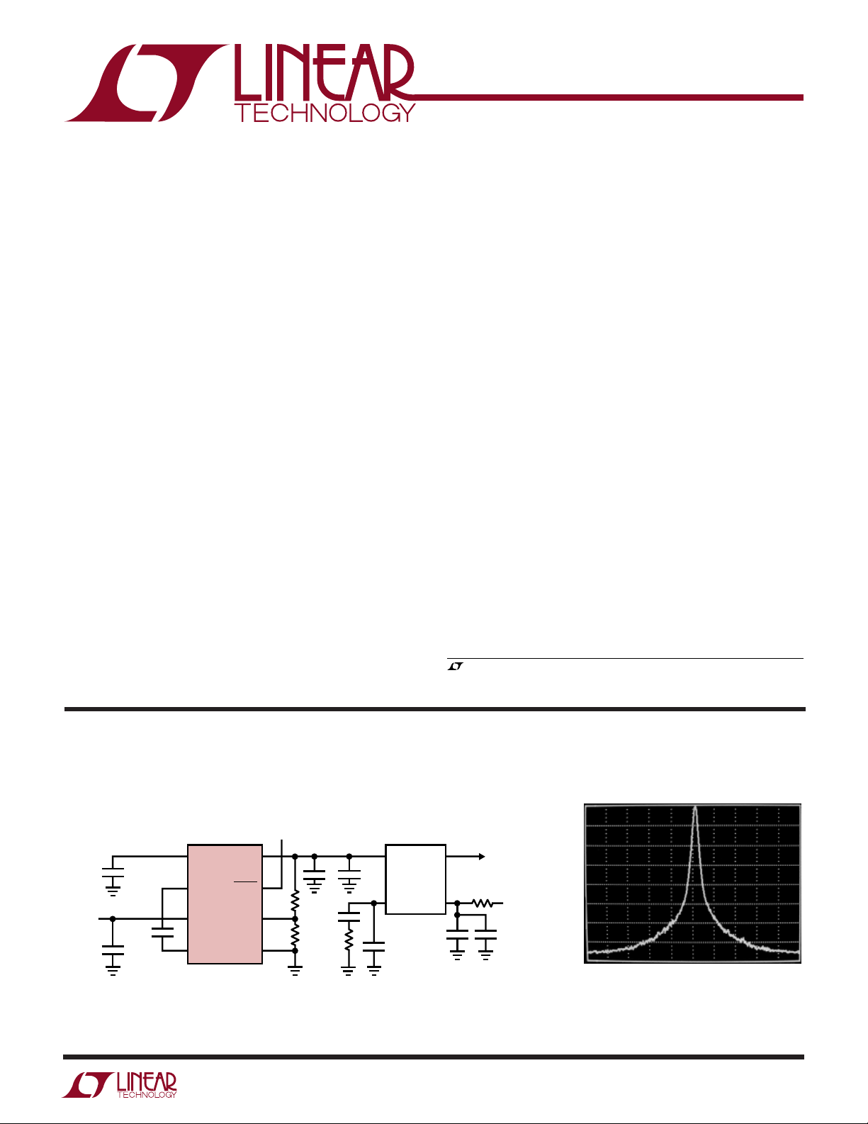
TYPICAL APPLICATIO
4.2V VCO Power Supply, VIN = 2.5V to 4.4V
SHUTDOWN
V
2.5V TO
4.4V
8
CPO
4.7µF
IN
0.22µF
4.7µF
7
C
6
V
5
C
+
LTC1682
IN
–
V
OUT
SHDN
GND
FB
U
Open-Loop Close-In Phase Noise
4.2V
1
2
3
4
36k
15k
4.7µF
1µF
1k
1000pF
B
VCO
MURATA
MQE001-902
M
1000pF
1000pF
P
C
100k
f
OUT
902MHz
V
4.7µF
1682 TA01
C
AMPLITUDE
10dB/DIV
CENTER = 902MHz RES BW = 1kHz
SPAN = 100kHz VBW = 30Hz
SWP = 10 sec REF = 0dBm
1682 TA02
1
Page 2
LTC1682/LTC1682-3.3/LTC1682-5
TOP VIEW
S8 PACKAGE
8-LEAD PLASTIC SO
1
2
3
4
8
7
6
5
V
OUT
SHDN
FILT/FB*
GND
CPO
C
+
V
IN
C
–
*PIN3 = FILT FOR LTC1682-3.3/LTC1682-5
= FB FOR LTC1682
WW
W
ABSOLUTE MAXIMUM RATINGS
U
(Note 1)
VIN to Ground ..............................................–0.3V to 5V
V
Voltage................................................–0.3V to 6V
OUT
CPO to Ground ........................................................ 10V
SHDN, FILT/FB Voltage to
Ground ..................................... – 0.3V to (VIN + 0.3V)
V
Short-Circuit Duration............................ Indefinite
OUT
I
...................................................................... 90mA
OUT
UUW
PACKAGE/ORDER INFORMATION
ORDER PART
NUMBER
TOP VIEW
V
1
OUT
2
SHDN
3
FILT/FB*
4
GND
MS8 PACKAGE
8-LEAD PLASTIC MSOP
*PIN3 = FILT FOR LTC1682-3.3/LTC1682-5
= FB FOR LTC1682
T
= 125°C, θJA = 140°C/ W
JMAX
8
CPO
+
7
C
V
6
IN
–
C
5
LTC1682CMS8
LTC1682CMS8-3.3
LTC1682CMS8-5
LTC1682IMS8
LTC1682IMS8-3.3
LTC1682IMS8-5
MS8 PART MARKING
LTER
LTGT
LTGV
LTHM
LTGU
LTGW
Operating Temperature Range
Commercial ............................................ 0°C to 70°C
Extended Commercial (Note 2)........... – 40°C to 85°C
Industrial ........................................... –40°C to 85°C
Storage Temperature Range ................. –65°C to 150°C
Lead Temperature (Soldering, 10 sec)..................300°C
Maximum Junction Temperature..........................125°C
ORDER PART
NUMBER
LTC1682CS8
LTC1682CS8-3.3
LTC1682CS8-5
LTC1682IS8
LTC1682IS8-3.3
LTC1682IS8-5
S8 PART MARKING
= 125°C, θJA = 120°C/W
T
JMAX
1682
168233
16825
1682I
1682I33
1682I5
Consult factory for Military grade parts.
ELECTRICAL CHARACTERISTICS
range, otherwise specifications are TA = 25°C. SHDN = VIN = 3V; C1 = 0.22µF; C2, C3, C4 = 4.7µF, unless otherwise noted.
PARAMETER CONDITIONS MIN TYP MAX UNITS
VIN Operating Voltage LTC1682 ● 1.8 4.4 V
I
Shutdown Current SHDN = 0V ● 15 µA
VIN
I
Operating Current I
VIN
FB Input Current LTC1682, FB = 1.235V ● –50 50 nA
FB Voltage LTC1682 ● 1.210 1.235 1.260 V
Regulated Output Voltage LTC1682-3.3, I
V
Temperature Coefficient ±50 ppm
OUT
Charge Pump Oscillator Frequency I
Burst Mode is a trademark of Linear Technology Corporation.
2
The ● denotes specifications that apply over the full operating temperature
LTC1682-3.3
LTC1682-5
= 0mA, Burst Mode
OUT
0°C to 70°C
–40°C to 85°C
LTC1682-5, I
> 200µA, VIN = 1.8V to 4.4V ● 480 550 620 kHz
OUT
OUT
OUT
TM
Operation
= 1mA ● 3.23 3.30 3.37 V
= 1mA ● 4.9 5.0 5.1 V
● 2 4.4 V
● 2.7 4.4 V
● 150 250 µA
● 150 300 µA
Page 3
LTC1682/LTC1682-3.3/LTC1682-5
ELECTRICAL CHARACTERISTICS
The ● denotes specifications that apply over the full operating temperature
range, otherwise specifications are TA = 25°C. SHDN = VIN = 3V; C1 = 0.22µF; C2, C3, C4 = 4.7µF, unless otherwise noted.
PARAMETER CONDITIONS MIN TYP MAX UNITS
CPO (Charge Pump Output) VIN = 1.8V, I
Output Resistance V
V
Dropout Voltage (Note 3) LTC1682, I
OUT
= 3V, I
IN
= 4.4V, I
V
IN
LTC1682/LTC1682-3.3, I
LTC1682/LTC1682-5, I
V
Enable Time I
OUT
V
Output Noise Voltage LTC1682 I
OUT
= 10mA 2 ms
OUT
LTC1682-3.3 I
LTC1682-5 I
V
Line Regulation VIN = 3V to 4V, I
OUT
V
Load Regulation I
OUT
V
Shutdown Resistance SHDN = 0V, Resistance Measured to Ground, VIN = 1.8V ● 150 350 Ω
OUT
= 1mA to 10mA ● 310 mV
OUT
I
= 1mA to 50mA (Note 4) 10 mV
OUT
SHDN = 0V, Resistance Measured to Ground, V
SHDN Input Threshold VIN = 1.8V to 4.4V ● 0.4 1 1.6 V
SHDN Input Current SHDN = V
SHDN = 0V
= 10mA ● 18 30 Ω
OUT
= 10mA ● 13 20 Ω
OUT
= 10mA ● 11 17 Ω
OUT
= 10mA, V
OUT
IN
OUT
I
OUT
OUT
I
OUT
OUT
I
OUT
= 0mA (Note 6) ● 520 mV
OUT
= 2.57V (Note 5) ● 100 160 mV
OUT
= 10mA, V
OUT
= 10mA, V
OUT
= 10mA, 10Hz ≤ f ≤ 100kHz, V
= 10mA, 10Hz ≤ f ≤ 2.5MHz, V
= 10mA, 10Hz ≤ f ≤ 100kHz, C
= 10mA, 10Hz ≤ f ≤ 2.5MHz, C
= 10mA, 10Hz ≤ f ≤ 100kHz, C
= 10mA, 10Hz ≤ f ≤ 2.5MHz, C
= 3.3V ● 75 120 mV
OUT
= 5V ● 50 90 mV
OUT
= 5V 88 µV
OUT
= 5V 800 µV
OUT
= 1nF 58 µV
FILT
= 1nF 500 µV
FILT
= 1nF 64 µV
FILT
= 1nF 600 µV
FILT
= 4.4V ● 50 150 Ω
IN
● –1 1 µA
● –1 1 µA
RMS
P-P
RMS
P-P
RMS
P-P
Note 1: Absolute Maximum Ratings are those values beyond which the life
of a device may be impaired.
Note 2: The LTC1682C is guaranteed to meet specified performance from
0°C to 70°C and is designed, characterized and expected to meet these
extended temperature limits, but is not tested at –40°C and 85°C. The
LTC1682I is guaranteed to meet the extended temperature limits.
Note 3: Dropout voltage is the minimum input/output voltage required to
maintain regulation at the specified output current. In dropout the output
voltage will be equal to: V
CPO
– V
DROPOUT
(see Figure 4).
Note 4: Operating conditions are limited by maximum junction
temperature. The regulated output specification will not apply for all
possible combinations of input voltage and output current. When
operating at maximum input voltage, the output current range may be
limited. When operating at maximum output current, the input voltage
range may be limited.
Note 5: Limited by the LDO disable switch point of 1.45V
.
IN
Note 6: The LTC1682 is set to 5V. The feedback current is 25µA.
3
Page 4
LTC1682/LTC1682-3.3/LTC1682-5
UW
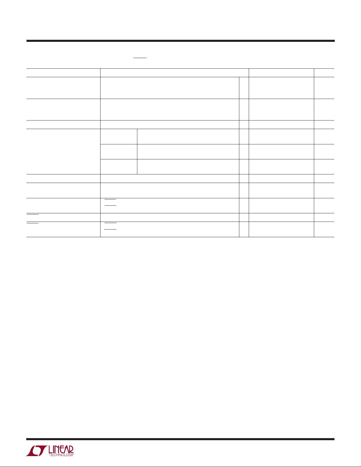
TYPICAL PERFOR A CE CHARACTERISTICS
CPO Output Resistance vs V
35
30
25
(Ω)
20
CPO
R
15
10
5
1.5
2.5 3.0 3.5
2.0
VIN (V)
LTC1682-5 Output Noise
(BW = 10Hz to 2.5MHz)
IN
TA = 25°C
C1 = 0.22µF
= 10mA
I
OUT
4.0 4.5
1682 G01
Min and Max V
9
TA = 25°C
8
7
6
(V)
CPO
V
5
4
3
1.5
(A) THE MAXIMUM GENERATED NO LOAD
(B) THE MINIMUM ALLOWABLE CPO VOLTAGE,
V
2.5 3.0 3.5
2.0
CPO VOLTAGE
AT FULL LOAD, TO ENSURE THAT THE LDO
IS NOT DISABLED
Shutdown to Enable Timing
CPO
vs V
CPO
= 2(VIN)
(A)
V
VIN (V)
IN
(B)
= 1.45(VIN)
CPO
4.0 4.5
1682 G02
V
Transient Response
OUT
10
5
(mV)I
0
OUT
TA = 25°C
∆V
(mA)
OUT
V
–5
IN
V
OUT
C
–10
OUT
15
10
5
0
050
= 3V
= 4V
= 10µF
100 200150
TIME (µs)
Enable to Shutdown Timing
250
300
1682 G02
V
OUT
200µV/DIV
C
= C
CPO
= 10mA TA = 25°C
I
OUT
= 3V C
V
IN
100µs/DIV 1682 G04
= 4.7µFV
OUT
Oscillator Frequency vs
Temperature
565
VIN = 3V
560
555
550
545
540
OSCILLATION FREQUENCY (kHz)
535
530
–50
= 5V
OUT
= 1nF
FILT
–25 0
50 100 125
25 75
TEMPERATURE (°C)
SHDN (V)V
(V)
OUT
2
0
4
3
2
1
0
1682 G07
TA = 25°C
= 3V
V
IN
= 4V
V
OUT
= 10mA
I
OUT
= C
C
CPO
OUT
= 10µF
200µs/DIV
1682 G05
Operating Current vs V
(No Load)
220
TA = 25°C
200
180
160
140
120
100
OPERATING CURRENT (µA)
80
60
1.5
LTC1682-3.3
LTC1682-5
2.5 3.0 3.5 4.0 4.5
2.0
2
0
SHDN (V)V
4
3
(V)
2
OUT
1
0
VIN (V)
NO LOAD
= 25°C
T
A
= 3V
V
IN
= 4V
V
OUT
= 10µF
C
OUT
IN
LTC1682
1ms/DIV
1682 G06
1682 G08
4
Page 5

LTC1682/LTC1682-3.3/LTC1682-5
UW
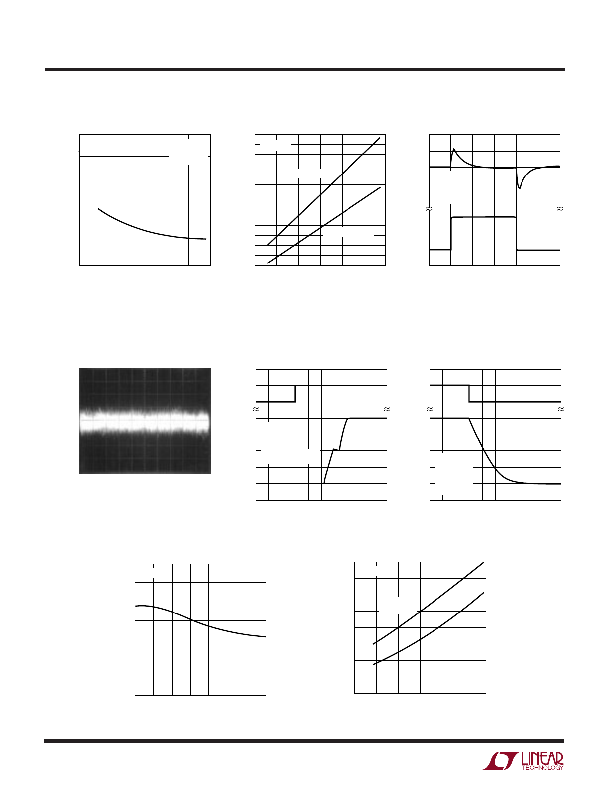
TYPICAL PERFOR A CE CHARACTERISTICS
V
Voltage vs Temperature
OUT
5.030
V
5.020
I
OUT
5.010
5.000
4.990
3.340
3.330
3.320
3.310
VOLTAGE (V)
3.300
OUT
V
3.290
1.240
1.238
1.236
1.234
–50
IN
= 3V
= 10mA
LTC1682-3.3
0
–25
TEMPERATURE (°C)
LTC1682-5
LTC1682
25
75
50 125
100
1682 G09
5.000
4.999
4.998
4.997
4.996
4.995
4.994
4.993
VOLTAGE (V)
3.300
OUT
3.299
V
3.298
3.297
3.296
3.295
3.294
UUU
PIN FUNCTIONS
V
Voltage vs Output Current
OUT
LTC1682-5
LTC1682-3.3
20
0
15 25 40 45 50
510
OUTPUT CURRENT (mA)
30 35
VIN = 3.3V
= 25°C
T
A
1682 G10
V
(Pin 1): Low Noise Regulated Output Voltage. V
OUT
OUT
should be bypassed with a ≥2µF low ESR capacitor as
close to the pin as possible for best performance. The V
OUT
range is 2.5V to 5.5V.
SHDN (Pin 2): Shutdown Input. A logic low on the SHDN
pin puts the part in shutdown mode. A logic high enables
the part. To continuously enable the part connect SHDN to
VIN. When the part is in shutdown, V
will be connected
OUT
to ground via a 100Ω switch and CPO will be high
impedance disconnected from VIN.
FB (Pin 3) (LTC1682): The voltage on this pin is compared
to the internal reference voltage (1.235V) by the error
amplifier to keep the output in regulation. An external
resistor divider is required between V
and FB to adjust
OUT
the output voltage.
FILT (Pin 3) (LTC1682-3.3/LTC1682-5): This pin is used
to filter the internal voltage reference. Typically a 1nF
capacitor is connected from FILT to ground.
GND (Pin 4): System Ground.
C– (Pin 5): Flying Capacitor Negative Input.
VIN (Pin 6): Input Voltage, 1.8V to 4.4V. VIN should be
bypassed with a ≥2µF low ESR capacitor as close to the
pin as possible for best performance. A minimum capacitance value of 0.1µF is required.
C+ (Pin 7): Flying Capacitor Positive Input.
CPO (Pin 8): Unregulated Charge Pump Output Voltage.
Approximately 1.95(VIN) at low loads. Bypass with a ≥2µF
low ESR capacitor. If a minimum V
required, the CPO capacitor should be 2× the V
enable time is
OUT
OUT
capacitor.
5
Page 6

LTC1682/LTC1682-3.3/LTC1682-5
W
BLOCK DIAGRA SM
C1
0.22µF
+
C
V
IN
C4
4.7µF
6
CHARGE PUMP
AND
SLEW CONTROL
57
CLK1
–
C
CPO
ENB
8
–
275k
C3
4.7µF
+
38k
1:100
+
–
328k
1
SD
100Ω
C2
4.7µF
V
OUT
SHDN
POWER-
2
ON
RESET
SD
REGEN
ENB
550kHz
OSCILLATOR
REG B
–
V
REF
= 1.235V
V
IN
+
LDO
REGEN
1µA/2µA
6
FB
34
GND
Figure 1. LTC1682 Block Diagram
R1
R2
1682 F01
Page 7

W
BLOCK DIAGRA SM
C1
0.22µF
LTC1682/LTC1682-3.3/LTC1682-5
V
IN
4.7µF
C4
SHDN
1nF
FILT
+
C
6
CHARGE PUMP
AND
SLEW CONTROL
57
CLK1
–
C
CPO
ENB
8
–
275k
C3
4.7µF
+
38k
1:100
+
–
328k
1
SD
100Ω
V
C2
4.7µF
OUT
POWER-
2
3
ON
RESET
REGEN
ENB
200k
V
SD
REF
= 1.235V
550kHz
OSCILLATOR
V
IN
RA
120k/65.5k
REG B
RB
200k
–
+
LDO
REGEN
1µA/2µA
4
GND
Figure 2. LTC1682-3.3/LTC1682-5 Block Diagram
1682 F02
7
Page 8

LTC1682/LTC1682-3.3/LTC1682-5
U
WUU
APPLICATIONS INFORMATION
Operation
The LTC1682 uses a switched-capacitor charge pump to
generate a CPO voltage of approximately 2(VIN). CPO
powers an internal low dropout linear regulator that supplies a regulated output at V
used to sense CPO and VIN voltages for power-up conditioning. The output current is sensed to determine the
charge pump operating mode. A trimmed internal bandgap
is used as the voltage reference and a trimmed internal
oscillator is used to control the charge pump switches.
The charge pump is a doubler configuration that uses one
external flying capacitor. When enabled, a 2-phase
nonoverlapping clock controls the charge pump switches.
At start-up, the LDO is disabled and the load is removed
from CPO. When CPO reaches 1.75(VIN) the LDO is
enabled. If CPO falls below 1.45(VIN) the LDO will be
disabled. Generally, the charge pump runs open loop with
continuous clocking for low noise. If CPO is greater than
1.95(VIN)
and
I
is less than 100µA, the charge pump
OUT
will operate in Burst Mode operation for increased efficiency but slightly higher output noise. In Burst Mode
operation, the clock is disabled when CPO reaches 1.95(VIN)
and enabled when CPO droops by about 100mV. The
switching frequency is precisely controlled to ensure that
the frequency is above 455kHz and at the optimum rate to
ensure maximum efficiency. The switch edge rates are
also controlled to minimize noise. The effective output
resistance at CPO is dependent on the voltage at VIN, CPO
and the junction temperature. A low ESR capacitor of ≥2µF
should be used at CPO for minimum noise.
. Internal comparators are
OUT
The LDO is used to filter the ripple on CPO and to set an
output voltage independent of CPO. V
is set by an
OUT
external or internal resistor divider. The LDO requires a
capacitor on V
for stability and improved load transient
OUT
response. A low ESR capacitor of ≥2µF should be used.
Output Voltage Selection
The LTC1682-3.3/LTC1682-5 versions have internal
resistor networks to set the regulated output voltage. The
LTC1682 output voltage is set using an external resistor
divider (see Figure 3). The output voltage is determined
using the following formula:
V
= 1.235V(1 + R1/R2)
OUT
The output voltage range is 2.5V to 5.5V.
Maximum V
OUT
and I
Calculations
OUT
The maximum available output voltage and current can be
calculated based on the open circuit CPO voltage, the
dropout voltage of the LDO and the effective output
resistance of the charge pump. The open circuit CPO
voltage is approximately 2(VIN) (see Figure 4).
R
+
2V
IN
–
CPO
V
CPO
Figure 4. Equivalent Circuit
R
DROPOUT
+
V
DROPOUT
C
CPO
V
OUT
–
I
LOAD
1682 F04
8
EXTERNAL LDO
C3
4.7µF
IN
3.3V
OUT
C5
GND
V
3.6V
IN
4.7µF
C4
0.22µF
8
CPO
7
+
C
LTC1682
6
V
C1
IN
5
–
C
V
OUT
SHDN
GND
1
2
R1
56k
3
FB
4
R2
18k
V
OUT
1682 F03
5.1V
V
= 800µV
RIPPLE
C2
4.7µF
= 1.235V(1 + R1/R2)
P-P
Figure 3. Powering an Auxiliary Regulator from CPO
Page 9

LTC1682/LTC1682-3.3/LTC1682-5
U
WUU
APPLICATIONS INFORMATION
The following formula can be used to find the maximum
output voltage that may be programmed for a given
minimum input voltage and output current load:
V
OUT(MAX)
with the condition that (I
Example:
V
IN(MIN)
I
= 10mA
OUT
R
CPO(MAX)
Max unloaded CPO voltage = 6V
Loaded CPO voltage = 6V – (10mA)(20Ω) = 5.8V
V
DROPOUT(MAX)
V
OUT(MAX)
V
< 5.5V and (I
OUT
For minimum noise applications, the LDO must be kept out
of dropout to prevent CPO noise from coupling into V
External CPO Loading
= (2)(V
IN(MIN)
OUT
) – (I
)(R
)(R
OUT
) < 0.55VIN.
CPO
= 3V
= 20Ω
= 0.08V
= (6V) – (0.2V) – (0.08V) = 5.72V
)(R
OUT
) < 0.55VIN, 0.2V < 1.65V.
CPO
CPO
) – V
DROPOUT
OUT
.
instantaneous currents which may induce ripple onto
a common voltage rail. C4 should be ≥2µF and a spike
reducing resistor of 2.2Ω may be required between
VIN and the supply.
A low ESR ceramic capacitor is recommended for the
flying capacitor C1 with a value of 0.22µF. At low load or
high VIN a smaller capacitor could be used to reduce ripple
on CPO which would reflect as lower ripple on V
OUT
.
If a minimum enable time is required, the CPO output filter
capacitor should be at least 2× the V
filter capacitor.
OUT
When the LDO is first enabled, the CPO capacitor will
dump a large amount of charge into the V
capacitor. If
OUT
the drop in the CPO voltage falls below 1.45(VIN), the LDO
will be disabled and the CPO voltage will have to charge up
to 1.75(VIN) to enable the LDO. The resulting cycling
extends the enable time.
A 1nF filter capacitor for the LTC1682-3.3/LTC1682-5
should be connected between the FILT pin and ground for
optimum noise performance.
The CPO output can drive an external load (an LDO, for
example). The current required by this additional load will
reduce the available current from V
requires 5mA, then the maximum available current at V
. If the external load
OUT
OUT
will be reduced by 5mA.
Short-Circuit and Thermal Protection
V
can be shorted to ground indefinitely. Internal cir-
OUT
cuitry will limit the output current. If the junction temperature exceeds 150°C, the part will shut down. Excessive
power dissipation due to heavy loads will also cause the
part to shut down when the junction temperature exceeds
150°C. The part will become enabled when the junction
temperature drops below 140°C. If the fault condition
remains in place, the part will cycle between the shutdown
and enabled states.
Capacitor Selection
For best performance it is recommended that low ESR
capacitors be used for C2, C3 and C4 in Figure 1 to
reduce noise and ripple. C2 must be ≥2µF and C3 must
be equal to or greater than C2. C4 is dependent on the
source impedance. The charge pump demands large
Output Ripple
The output noise and ripple on CPO includes a spike
component from the charge pump switches and a droop
component which is dependent on the load current and the
value of C3. The charge pump has been carefully designed
to minimize the spike component; however, low ESR
capacitors are essential to reduce the remaining spike
energy effect on the CPO voltage. C3 should be increased
for high load currents to minimize the droop component.
Ripple components on CPO are greatly reduced at V
OUT
by
the LDO; however, C2 should also be a low ESR capacitor
to improve filtering of the CPO noise.
Shutdown
When SHDN pin is pulled low (<0.4V), the part will be in
shutdown, the supply current will be < 5µA and V
OUT
will
be connected to ground through a 100Ω switch. In addition, CPO will be high impedance and disconnected from
VIN.
If shutdown is not required, connect SHDN to VIN which
will continuously enable the part.
9
Page 10

LTC1682/LTC1682-3.3/LTC1682-5
U
WUU
APPLICATIONS INFORMATION
Power-On Reset
Upon initial power-up, a power-on reset circuit ensures
that the internal functions are correctly initialized when
power is applied. Once VIN reaches approximately 1V, the
power-on reset circuit will enable the part as long as the
SHDN pin is held high.
Thermal Considerations
The power handling capability of the device will be limited
by the maximum rated junction temperature (125°C). The
device power dissipation PD = I
VIN(4mA). The device dissipates the majority of its heat
through its pins, especially GND (Pin 4). Thermal resistance to ambient can be optimized by connecting GND to
a large copper region on the PCB, which serves as a heat
sink. Applications which operate the LTC1682 near maximum power levels should maximize the copper area at all
pins except C+, C– and FILT/FB and ensure that there is
some airflow over the part to carry away excess heat.
(2VIN – V
OUT
OUT
) +
General Layout Considerations
Due to the high switching frequency and high transient
currents produced by the device, careful board layout is a
must. A clean board layout using a ground plane and short
connections to all capacitors will improve noise performance and ensure proper regulation (Figure 5).
The FILT pin on the LTC1682-3.3/LTC1682-5 is a high
impedance node. Leakage currents at this pin must be
minimized.
Measuring Output Noise
Measuring the LTC1682 low noise levels requires care.
Figure 6 shows a test setup for taking the measurement.
Good connection and signal handling technique should
yield about 500µV
over a 2.5MHz bandwidth. The noise
P-P
measurement involves AC coupling the LTC1682 output
into the test setup’s input and terminating this connection
with 50Ω. Coaxial connections must be maintained to
preserve measurement integrity.
BATTERY OR
LOW NOISE DC
POWER SUPPLY
R
LOAD
GROUND TERMINAL E5
BNC CABLES
OR COUPLERS
LTC1682
DEMO
BOARD
CONNECT BNC AND
GROUND TO THE
OUTPUT CAPACITOR
SHDN
COUPLING
CAPACITOR
V
OUT
R
LOAD
PLACE COUPLING
CAPACITOR IN SHIELDED
BOX WITH COAXIAL
CONNECTOR
V
OUT
C2
1
2
LTC1682-3.3/5
GND
3
4
C1
C
FILT
C3
8
V
IN
7
6
5
C4
1682 F05
Figure 5
PREAMPLIFIER
1822
+
R*
20dB
–
R*
*50Ω TERMINATIONS
HP-11048C OR
EQUIVALENT
BANDWIDTH
FILTER
R*
NOTE: KEEP BNC CONNECTIONS
AS SHORT AS POSSIBLE
INPUT
OSCILLOSCOPE
PLACE BANDWIDTH FILTER
COMPONENTS IN SHIELDED BOX
WITH COAXIAL CONNECTORS
1682 F06
10
Figure 6. LTC1682 Noise Measurement Test Setup
Page 11

TYPICAL APPLICATION
(
LTC1682/LTC1682-3.3/LTC1682-5
U
3.3V to Low Noise 3.3V Converter
SHUTDOWN
C3
4.7µF
V
IN
3.3V
C4
4.7µF
0.22µF
PACKAGE DESCRIPTION
0.007
(0.18)
0.021
± 0.006
(0.53 ± 0.015)
* DIMENSION DOES NOT INCLUDE MOLD FLASH, PROTRUSIONS OR GATE BURRS. MOLD FLASH,
PROTRUSIONS OR GATE BURRS SHALL NOT EXCEED 0.006" (0.152mm) PER SIDE
** DIMENSION DOES NOT INCLUDE INTERLEAD FLASH OR PROTRUSIONS.
INTERLEAD FLASH OR PROTRUSIONS SHALL NOT EXCEED 0.006"
° – 6° TYP
0
8
CPO
7
+
C
LTC1682-3.3
6
V
C1
IN
5
–
C
V
OUT
SHDN
FILT
GND
1
2
3
C
FILT
1nF
4
1682 TA03
C2
4.7µF
3.3V
V
RIPPLE
= 500µV
P-P
U
Dimensions in inches (millimeters) unless otherwise noted.
MS8 Package
8-Lead Plastic MSOP
(LTC DWG # 05-08-1660)
0.118 ± 0.004*
(3.00 ± 0.102)
0.040
SEATING
PLANE
± 0.006
(1.02 ± 0.15)
0.012
(0.30)
0.0256
REF
(0.65)
TYP
0.152mm) PER SIDE
0.034 ± 0.004
(0.86 ± 0.102)
0.006 ± 0.004
(0.15 ± 0.102)
0.192 ± 0.004
(4.88 ± 0.10)
8
7
12
6
5
0.118 ± 0.004**
(3.00 ± 0.102)
MSOP (MS8) 1197
4
3
8-Lead Plastic Small Outline (Narrow 0.150)
0.010 – 0.020
(0.254 – 0.508)
0.008 – 0.010
(0.203 – 0.254)
*
DIMENSION DOES NOT INCLUDE MOLD FLASH. MOLD FLASH
SHALL NOT EXCEED 0.006" (0.152mm) PER SIDE
**
DIMENSION DOES NOT INCLUDE INTERLEAD FLASH. INTERLEAD
FLASH SHALL NOT EXCEED 0.010" (0.254mm) PER SIDE
× 45°
0.016 – 0.050
0.406 – 1.270
0.053 – 0.069
(1.346 – 1.752)
0°– 8° TYP
0.014 – 0.019
(0.355 – 0.483)
S8 Package
(LTC DWG # 05-08-1610)
0.004 – 0.010
(0.101 – 0.254)
0.050
(1.270)
TYP
0.228 – 0.244
(5.791 – 6.197)
0.189 – 0.197*
(4.801 – 5.004)
7
8
1
2
5
6
0.150 – 0.157**
(3.810 – 3.988)
SO8 0996
3
4
11
Page 12

LTC1682/LTC1682-3.3/LTC1682-5
U
TYPICAL APPLICATION
Wide Input Range VCO Supply (VIN > 4.4V)
V
IN
3V TO 6V
Q1
FMMT3904
8
7
6
5
CPO
+
C
LTC1682-5
V
IN
–
C
(REQUIRED FOR
START-UP)
C3
4.7µF
D1
1N4148
3V
C4
4.7µF
0.22µF
C1
V
OUT
SHDN
FILT
GND
1
2
3
4
R1
470Ω
SHUTDOWN
C
1nF
FILT
LOW NOISE
C2
4.7µF
5V
VCO
1682 ta04
RELATED PARTS
PART NUMBER DESCRIPTION COMMENTS
LTC1340 Low Noise, Voltage-Boosted Varactor Driver Generates 5V Varactor Drive from 3V Supply
LTC1517-X Micropower, Regulated Charge Pump Doubler in SOT-23 ICC = 6µA; Short Circuit/Thermal Protected
LT1521 300mA Low Dropout Regulator Micropower; Good Transient Response
LTC1522 Micropower, Regulated 5V Charge Pump Ultralow Power: Typical Operating ICC = 6µA
LT1761 Series 100mA Low Noise LDO Regulator in SOT-23 ICC = 20µA; 20µV
Output Noise
RMS
12
Linear Technology Corporation
1630 McCarthy Blvd., Milpitas, CA 95035-7417
(408) 432-1900 ● FAX: (408) 434-0507
●
www.linear-tech.com
128235fs, sn128235 LT/TP 0799 4K • PRINTED IN USA
LINEAR TECHNOLOGY CORPORATION 1999
 Loading...