

Page 1
FEATURES
LTC1666/LTC1667/LTC1668
12-Bit, 14-Bit, 16-Bit,
U
50Msps DACs
DESCRIPTIO
■
50Msps Update Rate
■
Pin Compatible 12-Bit, 14-Bit and 16-Bit Devices
■
High Spectral Purity: 87dB SFDR at 1MHz f
■
5pV-s Glitch Impulse
■
Differential Current Outputs
■
20ns Settling Time
■
Low Power: 180mW from ±5V Supplies
■
TTL/CMOS (3.3V or 5V) Inputs
■
Small Package: 28-Pin SSOP
OUT
U
APPLICATIO S
■
Cellular Base Stations
■
Multicarrier Base Stations
■
Wireless Communication
■
Direct Digital Synthesis (DDS)
■
xDSL Modems
■
Arbitrary Waveform Generation
■
Automated Test Equipment
■
Instrumentation
The LTC®1666/LTC1667/LTC1668 are 12-/14-/16-bit,
50Msps differential current output DACs implemented on
a high performance BiCMOS process with laser trimmed,
thin-film resistors. The combination of a novel currentsteering architecture and a high performance process
produces DACs with exceptional AC and DC performance.
The LTC1668 is the first 16-bit DAC in the marketplace to
exhibit an SFDR (spurious free dynamic range) of 87dB
for an output signal frequency of 1MHz.
Operating from ±5V supplies, the
LTC1668
can be configured to provide full-scale output
LTC1666/LTC1667/
currents up to 10mA. The differential current outputs of
the DACs allow single-ended or true differential operation.
The –1V to 1V output compliance of the
LTC1667/LTC1668
allows the outputs to be connected
LTC1666/
directly to external resistors to produce a differential output voltage without degrading the converter’s linearity. Alternatively, the outputs can be connected to the summing
junction of a high speed operational amplifier, or to a
transformer.
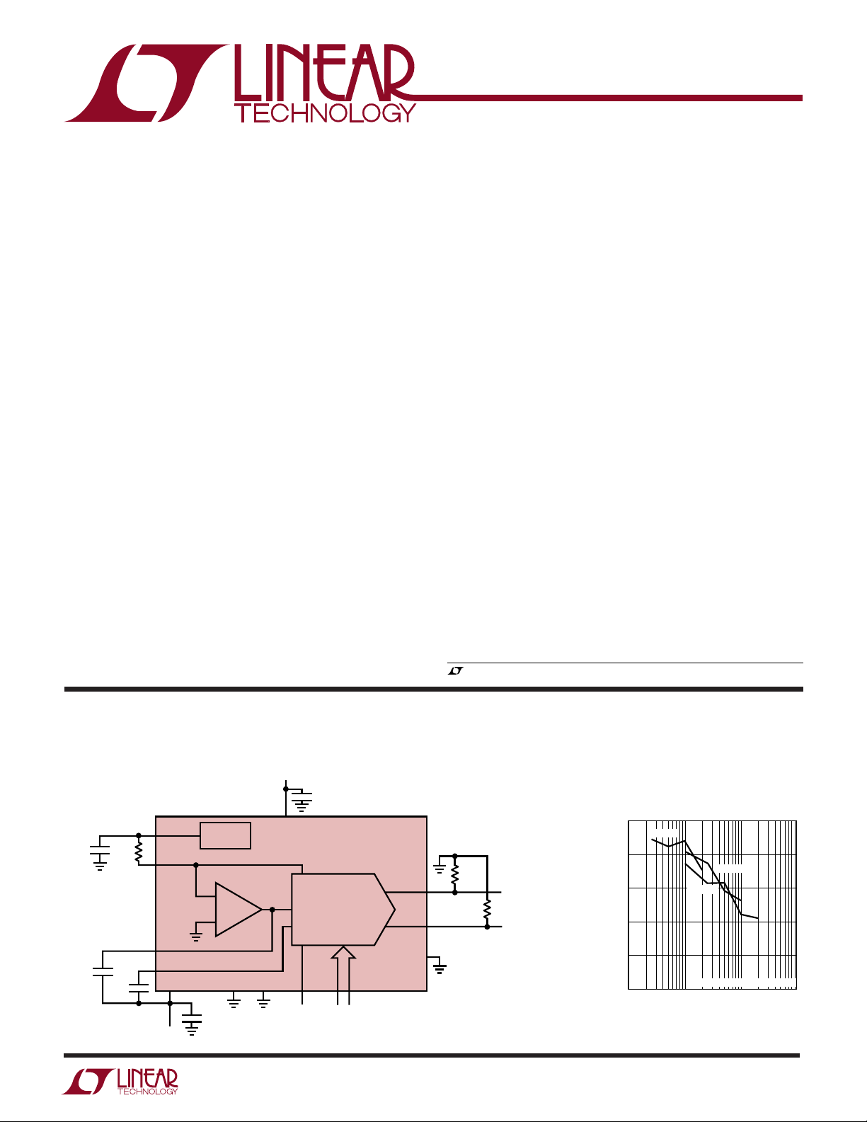
TYPICAL APPLICATION
LTC1668, 16-Bit, 50Msps DAC
5V
V
0.1µF
0.1µF
REFOUT
R
SET
2k
I
REFIN
COMP1
C1
C2
0.1µF
COMP2
V
SS
–5V
2.5V
REFERENCE
+
–
AGND DGND CLK DB15 DB0
0.1µF
U
DD
CLOCK
INPUT
0.1µF
16-BIT
HIGH SPEED
DAC
16-BIT DATA
INPUT
LTC1668
I
OUT A
I
OUT B
LADCOM
1666/7/8 TA01
The LTC1666/LTC1667/LTC1668 are pin compatible and
are available in a 28-pin SSOP and are fully specified over
the industrial temperature range.
, LTC and LT are registered trademarks of Linear Technology Corporation.
52.3Ω
52.3Ω V
+
1V
OUT
DIFFERENTIAL
–
LTC1668 SFDR vs f
100
5MSPS
90
80
P-P
SFDR (dB)
70
60
50
0.1
50MSPS
DIGITAL AMPLITUDE = 0dBFS
1.0 10 100
f
OUT
25MSPS
(MHz)
OUT
and f
CLOCK
1666/7/8 G05
1
Page 2
LTC1666/LTC1667/LTC1668
WWWU
ABSOLUTE AXI U RATI GS
(Note 1)
Supply Voltage (VDD)................................................ 6V
Negative Supply Voltage (VSS) ............................... – 6V
Total Supply Voltage (VDD to VSS) .......................... 12V
Digital Input Voltage ....................–0.3V to (VDD + 0.3V)
Analog Output Voltage
(I
OUT A
and I
) ........ (VSS – 0.3V) to (VDD + 0.3V)
OUT B
UU
W
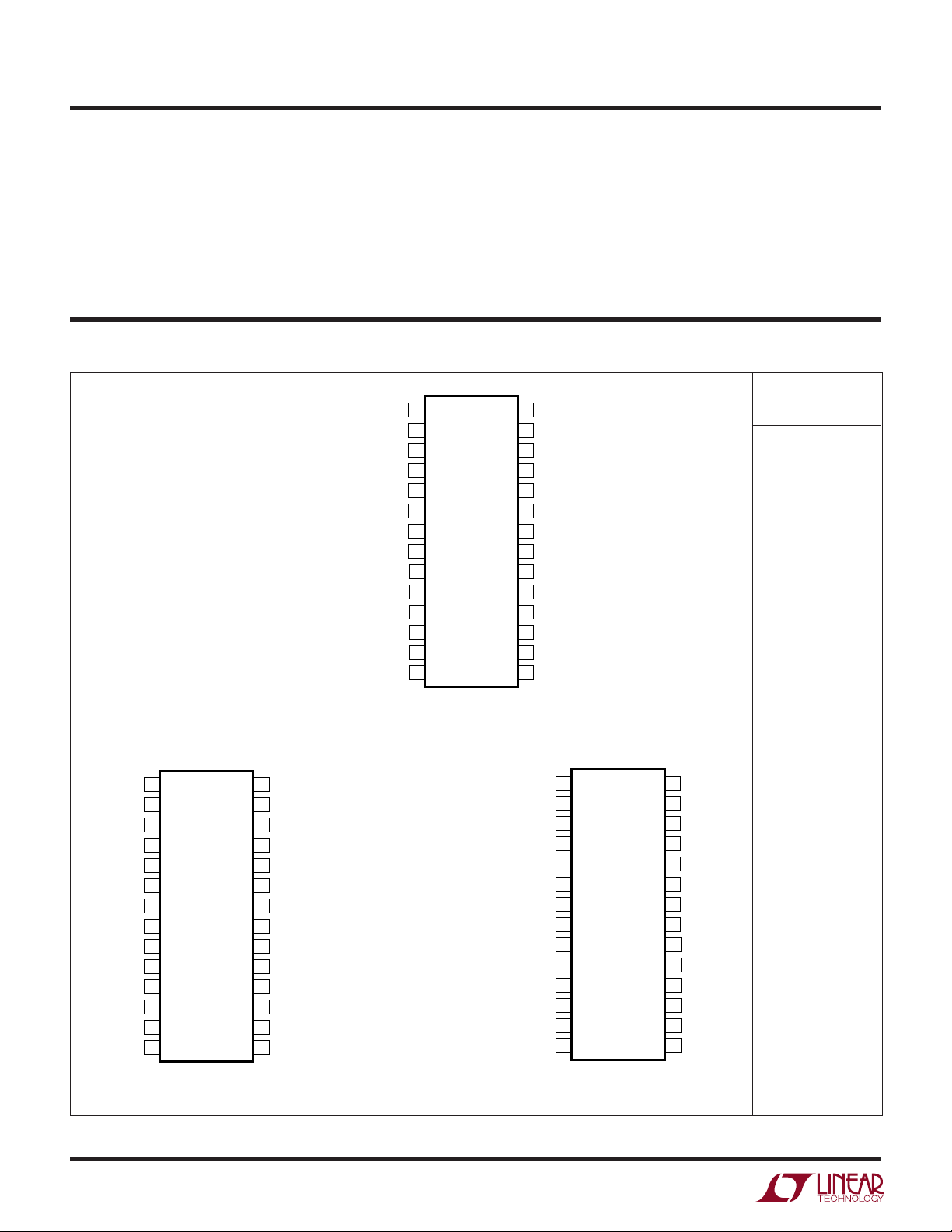
PACKAGE/ORDER I FOR ATIO
1
DB9
2
DB8
3
DB7
4
DB6
5
DB5
6
DB4
7
DB3
8
DB2
9
DB1
NC
NC
NC
NC
10
11
12
13
14
DB0 (LSB)
Power Dissipation............................................. 500mW
Operating Temperature Range
LTC1666C/LTC1667C/LTC1668C ........... 0°C to 70°C
LTC1666I/LTC1667I/LTC1668I.......... – 40°C to 85°C
Storage Temperature Range ................ –65°C to 150°C
Lead Temperature (Soldering, 10 sec).................. 300°C
TOP VIEW
DB10
28
DB11 (MSB)
27
CLK
26
V
25
DGND
24
V
23
COMP2
22
COMP1
21
I
20
I
19
LADCOM
18
AGND
17
I
16
REFOUT
15
DD
SS
OUT A
OUT B
REFIN
ORDER PART
NUMBER
LTC1666CG
LTC1666IG
G PACKAGE
28-LEAD PLASTIC SSOP
T
= 110°C, θJA = 100°C/W
JMAX
DB11
DB10
DB9
DB8
DB7
DB6
DB5
DB4
DB3
DB2
DB1
DB0 (LSB)
NC
NC
TOP VIEW
1
2
3
4
5
6
7
8
9
10
11
12
13
14
G PACKAGE
28-LEAD PLASTIC SSOP
T
= 110°C, θJA = 100°C/W T
JMAX
DB12
28
DB13 (MSB)
27
CLK
26
V
25
DGND
24
V
23
COMP2
22
COMP1
21
I
20
I
19
LADCOM
18
AGND
17
I
16
REFOUT
15
DD
SS
OUT A
OUT B
REFIN
ORDER PART
NUMBER
LTC1667CG
LTC1667IG
Consult LTC Marketing for parts specified with wider operating temperature ranges.
DB13
DB12
DB11
DB10
DB9
DB8
DB7
DB6
DB5
DB4
DB3
DB2
DB1
DB0 (LSB)
TOP VIEW
1
2
3
4
5
6
7
8
9
10
11
12
13
14
G PACKAGE
28-LEAD PLASTIC SSOP
= 110°C, θJA = 100°C/W
JMAX
DB14
28
DB15 (MSB)
27
CLK
26
V
25
DGND
24
V
23
COMP2
22
COMP1
21
I
20
I
19
LADCOM
18
AGND
17
I
16
REFOUT
15
DD
SS
OUT A
OUT B
REFIN
ORDER PART
NUMBER
LTC1668CG
LTC1668IG
2
Page 3
LTC1666/LTC1667/LTC1668
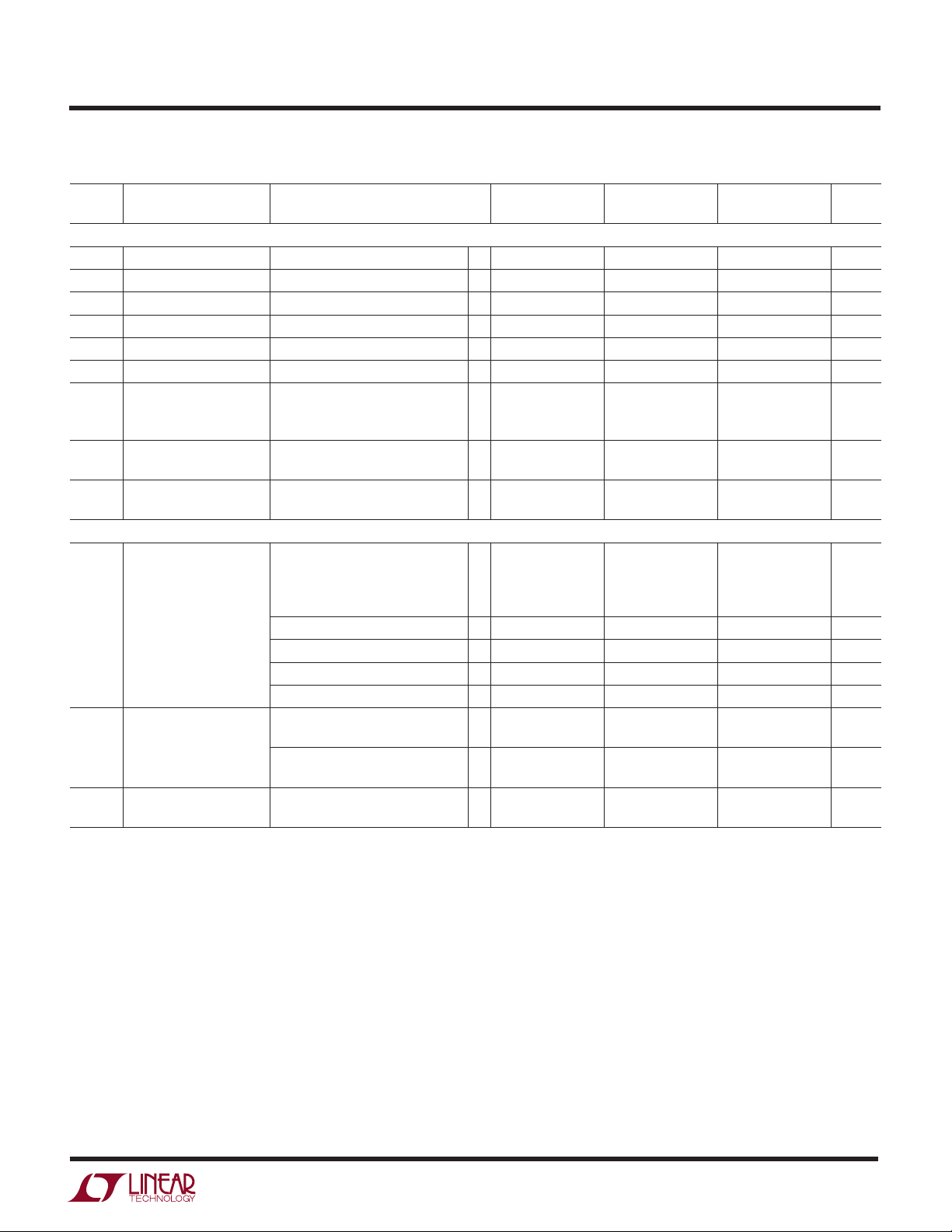
ELECTRICAL CHARACTERISTICS
temperature range, otherwise specifications are at TA = 25°C. VDD = 5V, VSS = –5V, LADCOM = AGND = DGND = 0V, I
The ● denotes specifications which apply over the full operating
= 10mA.
OUTFS
LTC1666 LTC1667 LTC1668
SYMBOL PARAMETER CONDITIONS MIN TYP MAX MIN TYP MAX MIN TYP MAX UNITS
DC Accuracy (Measured at I
, Driving a Virtual Ground)
OUT A
Resolution ● 12 14 16 Bits
Monotonicity 12 14 14 Bits
INL Integral Nonlinearity (Note 2) ±1 ±2 ±8 LSB
DNL Differential Nonlinearity (Note 2) ±1 ±1 ±1 ±4 LSB
Offset Error 0.1 ±0.2 0.1 ±0.2 0.1 ±0.2 % FSR
Offset Error Drift 5 5 5 ppm/°C
GE Gain Error Internal Reference, R
= 2k 2 2 2 % FSR
IREFIN
External Reference, 1 1 1 % FSR
V
REF
= 2.5V, R
IREFIN
= 2k
Gain Error Drift Internal Reference 50 50 50 ppm/°C
External Reference 30 30 30 ppm/°C
PSRR Power Supply VDD = 5V ±5% ±0.1 ±0.1 ±0.1 % FSR/V
Rejection Ratio V
= –5V ±5% ±0.2 ±0.2 ±0.2 % FSR/V
SS
AC Linearity
SFDR Spurious Free Dynamic f
= 25Msps, f
CLK
OUT
= 1MHz
Range to Nyquist 0dB FS Output 76 78 78 87 dB
–6dB FS Output 87 dB
–12dB FS Output 83 dB
f
Spurious Free Dynamic f
Range Within a Window f
THD Total Harmonic Distortion f
= 50Msps, f
CLK
f
= 50Msps, f
CLK
f
= 50Msps, f
CLK
f
= 50Msps, f
CLK
= 25Msps, 85 86 86 96 dB
CLK
= 1MHz, 2MHz Span
OUT
f
= 50Msps, 88 dB
CLK
= 5MHz, 4MHz Span
f
OUT
= 25Msps, f
CLK
= 50Msps, f
f
CLK
= 1MHz 85 dB
OUT
= 2.5MHz 81 dB
OUT
= 5MHz 79 dB
OUT
= 20MHz 70 dB
OUT
= 1MHz –75 –77 –84 – 77 dB
OUT
= 5MHz –78 dB
OUT
3
Page 4
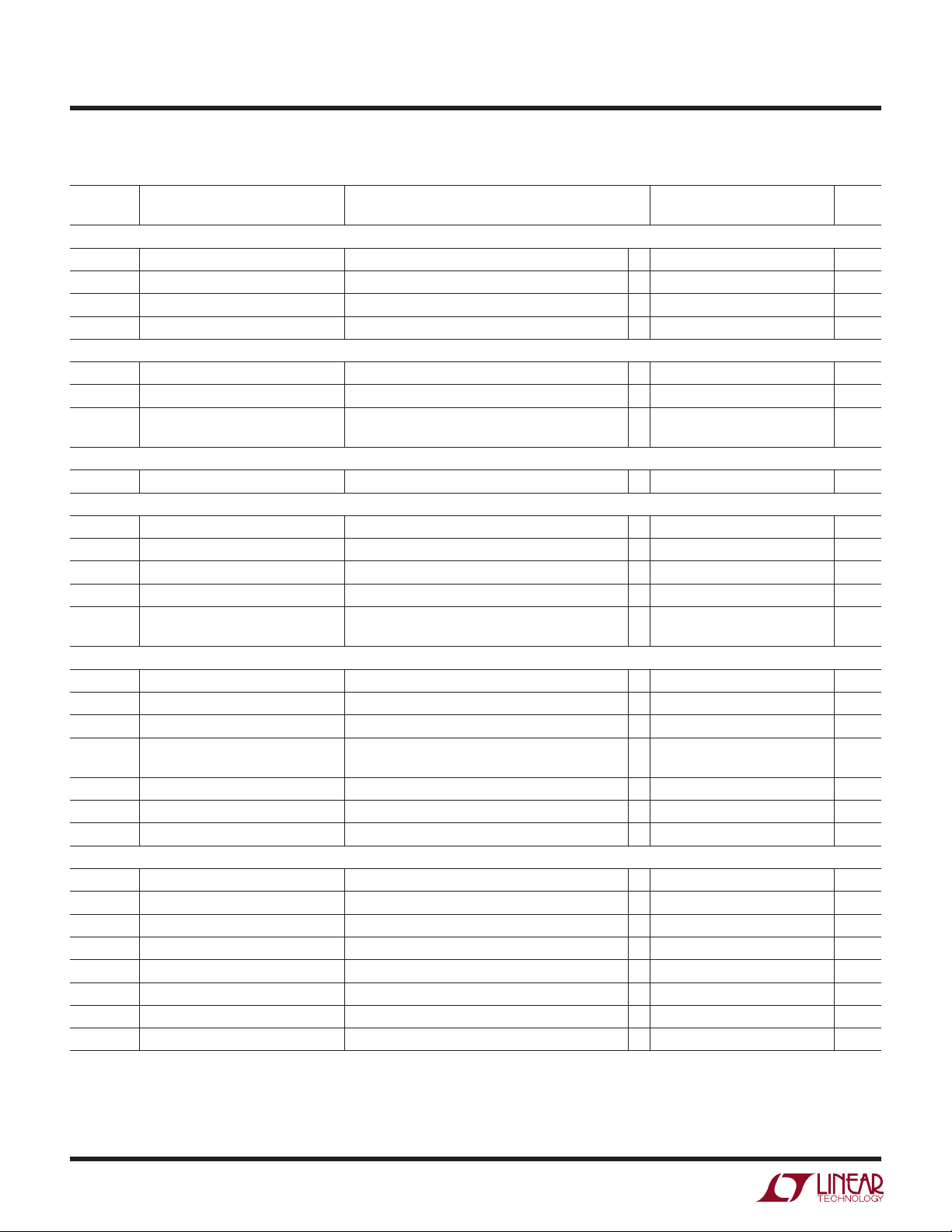
LTC1666/LTC1667/LTC1668
ELECTRICAL CHARACTERISTICS
temperature range, otherwise specifications are at TA = 25°C. VDD = 5V, VSS = –5V, LADCOM = AGND = DGND = 0V, I
The ● denotes specifications which apply over the full operating
= 10mA.
OUTFS
LTC1666/LTC1667/LTC1668
SYMBOL PARAMETER CONDITIONS MIN TYP MAX UNITS
Analog Output
I
OUTFS
Full-Scale Output Current ● 110mA
Output Compliance Range IFS = 10mA ● –1 1 V
Output Resistance; R
IOUT A
, R
IOUT BIOUT A, B
to LADCOM ● 0.7 1.1 1.5 kΩ
Output Capacitance 5pF
Reference Output
Reference Voltage REFOUT Tied to I
Through 2kΩ 2.475 2.5 2.525 V
REFIN
Reference Output Drift 25 ppm/°C
Reference Output Load Regulation I
= 0mA to 5mA 6 mV/mA
LOAD
Reference Input
Reference Small-Signal Bandwidth IFS = 10mA, C
= 0.1µF 20 kHz
COMP1
Power Supply
V
DD
V
SS
I
DD
I
SS
P
DIS
Positive Supply Voltage ● 4.75 5 5.25 V
Negative Supply Voltage ● –4.75 –5 –5.25 V
Positive Supply Current IFS = 10mA, f
Negative Supply Current IFS = 10mA, f
Power Dissipation IFS = 10mA, f
= 1mA, f
I
FS
= 25Msps, f
CLK
= 25Msps, f
CLK
= 25Msps, f
CLK
= 25Msps, f
CLK
= 1MHz ● 35mA
OUT
= 1MHz ● 33 40 mA
OUT
= 1MHz 180 mW
OUT
= 1MHz 85 mW
OUT
Dynamic Performance (Differential Transformer Coupled Output, 50Ω Double Terminated, Unless Otherwise Noted)
f
CLOCK
t
S
t
PD
Maximum Update Rate ● 50 75 Msps
Output Settling Time To 0.1% FSR 20 ns
Output Propagation Delay 8ns
Glitch Impulse Single Ended 15 pV-s
Differential 5 pV-s
t
r
t
f
i
NO
Output Rise Time 4ns
Output Fall Time 4ns
Output Noise 50 pA/√Hz
Digital Inputs
V
IH
V
IL
I
IN
C
IN
t
DS
t
DH
t
CLKH
t
CLKL
Note 1: Absolute Maximum Ratings are those values beyond which the life
of the device may be impaired.
Digital High Input Voltage ● 2.4 V
Digital Low Input Voltage ● 0.8 V
Digital Input Current ● ±10 µA
Digital Input Capacitance 5pF
Input Setup Time ● 8ns
Input Hold Time ● 4ns
Clock High Time ● 5ns
Clock Low Time ● 8ns
Note 2: For the LTC1666, ±1LSB = ±0.024% of full scale;
for the LTC1667, ±1LSB = ±0.006% of full scale = ±61ppm of full scale;
for the LTC1668, ±1LSB = ±0.0015% of full scale = ±15.3ppm of full scale.
4
Page 5
LTC1666/LTC1667/LTC1668
f
OUT
(MHz)
0
SFDR (dB)
10
95
90
85
80
75
70
65
60
55
50
1666/7/8 G09
2.5 5 7.5
DIGITAL AMPLITUDE = 0dBFS
I
OUTFS
= 2.5mA
I
OUTFS
= 5mA
I
OUTFS
= 10mA
UW
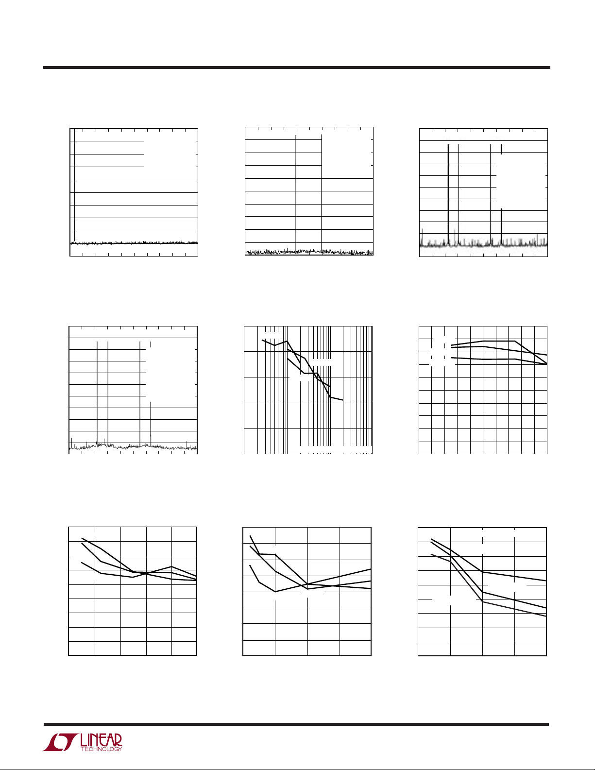
TYPICAL PERFOR A CE CHARACTERISTICS
(LTC1668)
Single Tone SFDR at 50MSPS 2-Tone SFDR
0
–10
–20
–30
–40
–50
–60
–70
SIGNAL AMPLITUDE (dBFS)
–80
–90
–100
05
FREQUENCY (MHz)
4-Tone SFDR, f
0
–10
–20
–30
–40
–50
–60
–70
–80
SIGNAL AMPLITUDE (dBFS)
–90
–100
–110
0.1 0.46 0.82 1.18 1.54 1.9
FREQUENCY (MHz)
10
CLOCK
SFDR = 87dB
f
CLOCK
= 1.002MHz
f
OUT
AMPL = 0dBFS
15 20 25
= 5MSPS
SFDR > 82dB
f
CLOCK
f
OUT1
f
OUT2
f
OUT3
f
OUT4
AMPL = 0dBFS
= 50MSPS
= –8.25dBm
1666/7/8 G01
= 5MSPS
= 0.5MHz
= 0.65MHz
= 1.10MHz
= 1.25MHz
1666/7/8 G04
0
–10
–20
–30
–40
–50
–60
–70
SIGNAL AMPLITUDE (dBFS)
–80
–90
–100
4.5 5.0 5.5
SFDR vs f
100
90
80
SFDR (dB)
70
60
50
0.1
SFDR > 86dB
f
CLOCK
f
OUT1
f
OUT2
AMPL = 0dBFS
FREQUENCY (MHz)
and f
OUT
5MSPS
1.0 10 100
CLOCK
25MSPS
50MSPS
DIGITAL AMPLITUDE = 0dBFS
f
(MHz)
OUT
= 50MSPS
= 4.9MHz
= 5.09MHz
1666/7/8 G02
1666/7/8 G05
4-Tone SFDR, f
0
–10
–20
–30
–40
–50
–60
–70
–80
SIGNAL AMPLITUDE (dBFS)
–90
–100
–110
1 4.6 8.2 11.8 15.4 19
FREQUENCY (MHz)
SFDR vs f
(dBFS) at f
100
95
90
85
80
75
SFDR (dB)
70
65
60
55
50
0 0.4
0dBFS
–6dBFS
–12dBFS
and Digital Amplitude
OUT
CLOCK
0.8
CLOCK
= 5MSPS
1.2 1.6 2.0
f
(MHz)
OUT
= 50MSPS
SFDR > 74dB
f
CLOCK
f
OUT1
f
OUT2
f
OUT3
f
OUT4
AMPL = 0dBFS
= 50MSPS
= 5.02MHz
= 6.51MHz
= 11.02MHz
= 12.51MHz
1666/7/8 G03
1666/7/8 G06
SFDR vs f
(dBFS) at f
95
90
85
80
75
70
SFDR (dB)
65
60
55
50
0dBFS
–6dBFS
–12dBFS
0
and Digital Amplitude
OUT
= 25MSPS
CLOCK
26
4
f
(MHz)
OUT
8
1666/7/8 G07
SFDR vs f
(dBFS) at f
90
85
80
75
70
SFDR (dB)
65
60
55
10
50
–12dBFS
0
and Digital Amplitude
OUT
= 50MSPS
CLOCK
0dBFS
–6dBFS
515
f
OUT
10
(MHz)
20
1666/7/8 G08
SFDR vs f
f
= 25MSPS
CLOCK
OUT
and I
OUTFS
at
5
Page 6
LTC1666/LTC1667/LTC1668
100mV
/DIV
CLK IN
5V/DIV
1666/7/8 G12
5ns/DIV
V(I
OUTB
)
V(I
OUTA
)
FFFF
0000
CLOCK INPUT
UW
TYPICAL PERFOR A CE CHARACTERISTICS
(LTC1668)
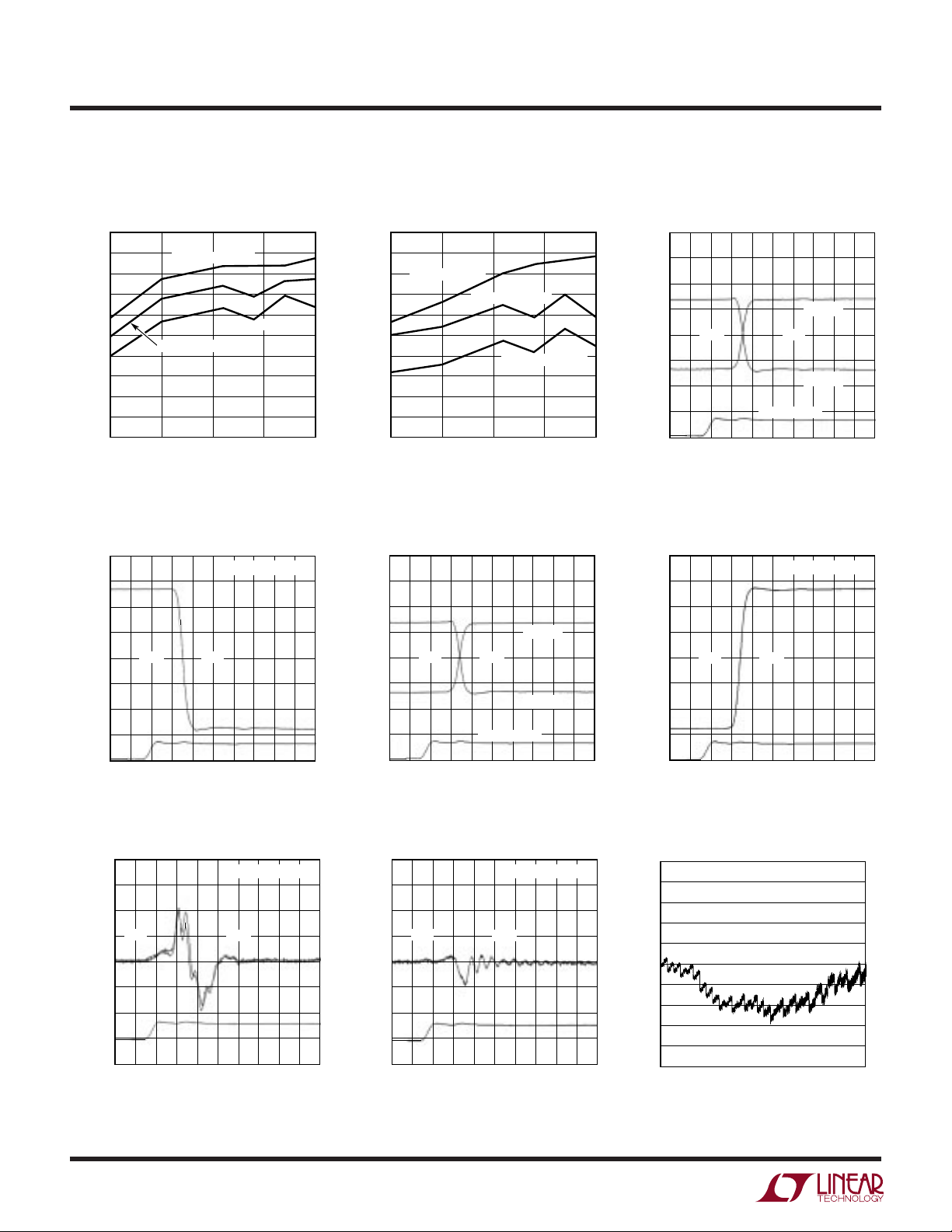
SFDR vs Digital Amplitude (dBFS)
and f
100
95
90
85
80
75
SFDR (dB)
70
65
60
55
50
–20 –15 –10 –5 0
at f
CLOCK
2.277MHz AT 25MSPS
DIGITAL AMPLITUDE (dBFS)
= f
OUT
CLOCK
455kHz AT 5MSPS
4.55MHz AT 50MSPS
Differential Output
Full-Scale Transition
V(I
OUTA
100mV
/DIV
0000
FFFF
/11
) – V(I
1666/7/8 G10
OUTB
SFDR vs Digital Amplitude (dBFS)
and f
100
95
90
85
80
75
SFDR (dB)
70
65
60
55
50
–20 –15 –10 –5 0
at f
CLOCK
1MHz AT 5MSPS
DIGITAL AMPLITUDE (dBFS)
= f
OUT
5MHz AT 25MSPS
/5
CLOCK
10MHz AT 50MSPS
1666/7/8 G11
Single-Ended Output
Full-Scale Transition
)
V(I
)
OUTA
100mV
/DIV
FFFF
0000
Single-Ended Outputs
Full-Scale Transition
Differential Output
Full-Scale Transition
100mV
/DIV
FFFF
0000
V(I
OUTA
) – V(I
OUTB
)
CLK IN
5V/DIV
Single-Ended Midscale
Glitch Impulse
7FFF
1mV/DIV
CLK IN
5V/DIV
5ns/DIV
5ns/DIV
V(I
8000
OUTA
), V(I
1666/7/8 G13
OUTB
1666/7/8 G16
V(I
)
OUTB
CLK IN
5V/DIV
CLOCK INPUT
5ns/DIV
1666/7/8 G14
CLK IN
5V/DIV
5ns/DIV
1666/7/8 G15
Differential Midscale
Glitch Impulse
)
7FFF
1mV/DIV
CLK IN
5V/DIV
8000
5ns/DIV
V(I
OUTA
) – V(I
)
OUTB
1666/7/8 G17
Integral Nonlinearity
5
4
3
2
1
0
–1
–2
–3
INTEGRAL NONLINEARITY (LSB)
–4
–5
16384
32768
DIGITAL INPUT CODE
49152
65535
1666/7/8 G18
6
Page 7
LTC1666/LTC1667/LTC1668
UW
TYPICAL PERFOR A CE CHARACTERISTICS
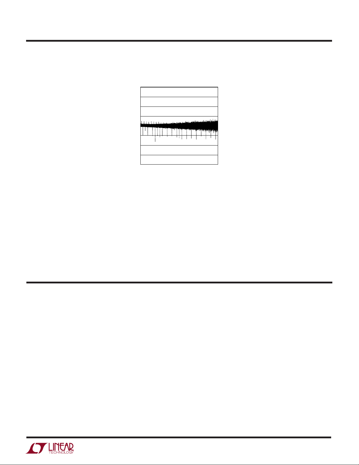
Differential Nonlinearity
2.0
1.5
1.0
0.5
0
–0.5
–1.0
DIFFERENTIAL NONLINEARITY (LSB)
–1.5
–2.0
0
16384
32768
DIGITAL INPUT CODE
49152
1666/7/8 G19
(LTC1668)
65535
U
UU
PI FU CTIO S
LTC1666
REFOUT (Pin 15): Internal Reference Voltage Output.
Nominal value is 2.5V. Requires a 0.1µF bypass capacitor
to AGND.
I
(Pin 16): Reference Input Current. Nominal value is
REFIN
1.25mA for IFS = 10mA. IFS = I
AGND (Pin 17): Analog Ground.
LADCOM (Pin 18): Attenuator Ladder Common. Normally
tied to GND.
I
(Pin 19): Complementary DAC Output Current. Full-
OUT B
scale output current occurs when all data bits are 0s.
I
(Pin 20): DAC Output Current. Full-scale output
OUT A
current occurs when all data bits are 1s.
REFIN
• 8.
COMP1 (Pin 21): Current Source Control Amplifier Compensation. Bypass to VSS with 0.1µF.
COMP2 (Pin 22): Internal Bypass Point. Bypass to V
SS
with 0.1µF.
VSS (Pin 23): Negative Supply Voltage. Nominal value is
–5V.
DGND (Pin 24): Digital Ground.
VDD (Pin 25): Positive Supply Voltage. Nominal value is 5V.
CLK (Pin 26): Clock Input. Data is latched and the output
is updated on positive edge of clock.
DB11 to DB0 (Pins 27, 28, 1 to 10 ): Digital Input Data Bits.
7
Page 8

LTC1666/LTC1667/LTC1668
U
UU
PI FU CTIO S
LTC1667
REFOUT (Pin 15): Internal Reference Voltage Output.
Nominal value is 2.5V. Requires a 0.1µF bypass capacitor
to AGND.
I
(Pin 16): Reference Input Current. Nominal value is
REFIN
1.25mA for IFS = 10mA. IFS = I
AGND (Pin 17): Analog Ground.
LADCOM (Pin 18): Attenuator Ladder Common. Normally
tied to GND.
I
(Pin 19): Complementary DAC Output Current. Full-
OUT B
scale output current occurs when all data bits are 0s.
I
(Pin 20): DAC Output Current. Full-scale output
OUT A
current occurs when all data bits are 1s.
COMP1 (Pin 21): Current Source Control Amplifier Com-
pensation. Bypass to VSS with 0.1µF.
REFIN
• 8.
LTC1668
REFOUT (Pin 15): Internal Reference Voltage Output.
Nominal value is 2.5V. Requires a 0.1µF bypass capacitor
to AGND.
I
(Pin 16): Reference Input Current. Nominal value is
REFIN
1.25mA for IFS = 10mA. IFS = I
AGND (Pin 17): Analog Ground.
LADCOM (Pin 18): Attenuator Ladder Common. Normally
tied to GND.
I
(Pin 19): Complementary DAC Output Current. Full-
OUT B
scale output current occurs when all data bits are 0s.
I
(Pin 20): DAC Output Current. Full-scale output
OUT A
current occurs when all data bits are 1s.
COMP1 (Pin 21): Current Source Control Amplifier Com-
pensation. Bypass to VSS with 0.1µF.
REFIN
• 8.
COMP2 (Pin 22): Internal Bypass Point. Bypass to V
with 0.1µF.
VSS (Pin 23): Negative Supply Voltage. Nominal value is
–5V.
DGND (Pin 24): Digital Ground.
VDD (Pin 25): Positive Supply Voltage. Nominal value is 5V.
CLK (Pin 26): Clock Input. Data is latched and the output
is updated on positive edge of clock.
DB13 to DB0 (Pins 27, 28, 1 to 12 ): Digital Input Data Bits.
SS
COMP2 (Pin 22): Internal Bypass Point. Bypass to V
with 0.1µF.
VSS (Pin 23): Negative Supply Voltage. Nominal value is
–5V.
DGND (Pin 24): Digital Ground.
VDD (Pin 25): Positive Supply Voltage. Nominal value is 5V.
CLK (Pin 26): Clock Input. Data is latched and the output
is updated on positive edge of clock.
DB15 to DB0 (Pins 27, 28, 1 to 14 ): Digital Input Data Bits.
SS
8
Page 9

BLOCK DIAGRA
0.1µF
V
REF
REFOUT
15
R
SET
2k
I
REFIN
16
W
2.5V
REFERENCE
IFS/8
LTC1666
5V
25
V
DD
ATTENUATOR
LADDER
LSB SWITCHES
LTC1666/LTC1667/LTC1668
0.1µF
18
LADCOM
20
19
52.3Ω 52.3Ω
+
–
V
OUT
1V
P-P
DIFFERENTIAL
SEGMENTED SWITCHES
FOR DB15–DB12
I
OUT A
I
OUT B
0.1µF
0.1µF
V
REF
R
2k
0.1µF
SET
+
–
COMP121
22
COMP2
V
SS
23
–5V
0.1µF
I
INT
AGND17DGND
CLK DB0DB11 • • •
24
26 27 10
CLOCK
INPUT
CURRENT SOURCE ARRAY
• • • • • •
INPUT LATCHES
• • •
12-BIT
DATA INPUT
1666 BD
LTC1667
5V
0.1µF
25
V
15
16
REFOUT
I
REFIN
2.5V
REFERENCE
IFS/8
DD
ATTENUATOR
LADDER
LSB SWITCHES
SEGMENTED SWITCHES
FOR DB15–DB12
LADCOM
I
OUT A
I
OUT B
18
20
19
52.3Ω 52.3Ω
+
–
V
OUT
1V
P-P
DIFFERENTIAL
0.1µF
0.1µF
+
–
COMP121
22
COMP2
V
SS
23
–5V
0.1µF
I
INT
AGND17DGND
CLK DB0DB13 • • •
24
26 27 12
CLOCK
INPUT
CURRENT SOURCE ARRAY
• • • • • •
INPUT LATCHES
• • •
14-BIT
DATA INPUT
1667 BD
9
Page 10

LTC1666/LTC1667/LTC1668
W
BLOCK DIAGRA
0.1µF
V
REF
REFOUT
15
R
SET
2k
I
REFIN
16
2.5V
REFERENCE
IFS/8
LTC1668
5V
25
V
DD
ATTENUATOR
LADDER
LSB SWITCHES
0.1µF
SEGMENTED SWITCHES
FOR DB15–DB12
LADCOM
I
OUT A
I
OUT B
18
20
19
52.3Ω 52.3Ω
+
–
V
OUT
1V
P-P
DIFFERENTIAL
COMP121
22
0.1µF
COMP2
0.1µF
–5V
UWW
TI I G DIAGRA
+
–
23
V
SS
0.1µF
I
INT
AGND17DGND
DATA
INPUT
CLK
24
N – 1
CURRENT SOURCE ARRAY
• • • • • •
INPUT LATCHES
CLK DB0DB15 • • •
26 27 14
CLOCK
INPUT
t
CLKL
t
DS
• • •
16-BIT
DATA INPUT
N N + 1
1668 BD
t
DH
t
CLKH
t
ST
t
PD
10
I
OUT A/IOUT B
N – 1 N
0.1%
1666/7/8 TD
Page 11

WUUU
APPLICATIO S I FOR ATIO
LTC1666/LTC1667/LTC1668
Theory of Operation
The
LTC1666/LTC1667/LTC1668
are high speed current
steering 12-/14-/16-bit DACs made on an advanced
BiCMOS process. Precision thin film resistors and well
matched bipolar transistors result in excellent DC linearity
and stability. A low glitch current switching design gives
excellent AC performance at sample rates up to 50Msps.
The devices are complete with a 2.5V internal bandgap
reference and edge triggered latches, and set a new
standard for DAC applications requiring very high dynamic range at output frequencies up to several megahertz.
Referring to the Block Diagrams, the DACs contain an
array of current sources that are steered to I
OUTA
or I
OUTB
with NMOS differential current switches. The four most
significant bits are made up of 15 current segments of
equal weight. The remaining lower bits are binary weighted,
using a combination of current scaling and a differential
resistive attenuator ladder. All bits and segments are
precisely matched, both in current weight for DC linearity,
and in switch timing for low glitch impulse and low
spurious tone AC performance.
Setting the Full-Scale Current, I
OUTFS
The reference control loop requires a capacitor on the
COMP1 pin for compensation. For optimal AC performance, C
should be connected to VSS and be placed
COMP1
very close to the package (less than 0.1").
For fixed reference voltage applications, C
COMP1
should
be 0.1µF or more. The reference control loop small-signal
bandwidth is approximately 1/(2π) • C
for C
COMP1
= 0.1µF.
COMP1
• 80 or 20kHz
Reference Operation
The onboard 2.5V bandgap voltage reference drives the
REFOUT pin. It is trimmed and specified to drive a 2k
resistor tied from REFOUT to I
1.25mA load (I
= 10mA). REFOUT has nominal
OUTFS
, corresponding to a
REFIN
output impedance of 6Ω, or 0.24% per mA, so it must be
buffered to drive any additional external load. A 0.1µF
capacitor is required on the REFOUT pin for compensation. Note that this capacitor is required for stability, even
if the internal reference is not being used.
External Reference Operation
Figure 1, shows how to use an external reference to control
the LTC1666/LTC1667/LTC1668 full-scale current.
The full-scale DAC output current, I
, is nominally
OUTFS
10mA, and can be adjusted down to 1mA. Placing a
resistor, R
sets I
OUTFS
, between the REFOUT pin, and the I
SET
as follows.
REFIN
pin
The internal reference control loop amplifier maintains a
virtual ground at I
source, I
I
is a scaled replica of the DAC current sources and
INT
I
OUTFS
I
OUTFS
, to sink the exact current flowing into I
INT
= 8 • (I
= 8 • (I
), therefore:
INT
REFIN
For example, if R
2.5V, I
= 2.5/2k = 1.25mA and I
REFIN
by servoing the internal current
REFIN
) = 8 • (V
= 2k and is tied to V
SET
REF/RSET
) (1)
REF
= 8 • (1.25mA)
OUTFS
REFIN
= REFOUT =
.
= 10mA.
REFOUT
5V
EXTERNAL
REFERENCE
Figure 1. Using the LTC1666/LTC1667/LTC1668
with an External Reference
0.1µF
R
SET
2.5V
REFERENCE
I
REFIN
+
–
LTC1666/
LTC1667/
LTC1668
1666/7/8 F02
11
Page 12

LTC1666/LTC1667/LTC1668
WUUU
APPLICATIO S I FOR ATIO
Adjusting the Full-Scale Output
In Figure 2, a serial interfaced DAC is used to set I
The LTC1661 is a dual 10-bit V
voltage output that swings from 0V to V
5V
REF
1/2 LTC1661
Figure 2. Adjusting the Full-Scale Current of
the LTC1666/LTC1667/LTC1668 with a DAC
0.1µF
DAC with a buffered
OUT
.
REF
2.5V
REFERENCE
LTC1666/
REFIN
LTC1667/
+
–
R
1.9k
I
SET
LTC1668
1666/7/8 F03
OUTFS
.
DAC Transfer Function
The LTC1666/LTC1667/LTC1668 use straight binary digital
coding. The complementary current outputs, I
, sink current from 0 to I
B
nal), I
swings from 0mA when all bits are low (e.g.,
OUT A
OUTFS
. For I
= 10mA (nomi-
OUTFS
OUT A
and I
OUT
Code␣ = 0) to 10mA when all bits are high (e.g., Code = 65535
for LTC1668) (decimal representation). I
mentary to I
OUT A
. I
OUT A
and I
are given by the following
OUT B
is comple-
OUT B
formulas:
LTC1666:
I
OUT A
I
OUT B
= I
= I
• (DAC Code/4096) (2)
OUTFS
• (4095 – DAC Code)/4096 (3)
OUTFS
LTC1667:
I
OUT A
I
OUT B
= I
= I
• (DAC Code/16384) (4)
OUTFS
• (16383 – DAC Code)/16384 (5)
OUTFS
LTC1668:
V
OUT A
V
OUT B
= I
= I
OUT A
OUT B
• R
• R
LOAD
LOAD
(8)
(9)
The differential voltage is:
V
= V
DIFF
= (I
Substituting the values found earlier for I
I
(LTC1668):
OUTFS
V
= {2 • DAC Code – 65535)/65536} • 8 •
DIFF
(R
LOAD/RSET
OUT A
OUT A
) • (V
– V
– I
OUT B
) • (R
OUT B
) (11)
REF
LOAD
)
, I
OUT A
OUT B
(10)
and
From these equations some of the advantages of differential mode operation can be seen. First, any common mode
noise or error on I
OUT A
and I
is cancelled. Second, the
OUT B
signal power is twice as large as in the single-ended case.
Third, any errors and noise that multiply times I
I
, such as reference or I
OUT B
noise, cancel near
OUTFS
OUT A
and
midscale, where AC signal waveforms tend to spend the
most time. Fourth, this transfer function is bipolar; e.g. the
output swings positive and negative around a zero output
at mid-scale input, which is more convenient for AC
applications.
Note that the term (R
LOAD/RSET
) appears in both the
differential and single-ended transfer functions. This means
that the Gain Error of the DAC depends on the ratio of
R
to R
LOAD
temperature tracking of R
the absolute tempco of R
, and the Gain Error tempco is affected by the
SET
with R
LOAD
is very critical for DC
LOAD
. Note also that
SET
nonlinearity. As the DAC output changes from 0mA to
10mA the R
resistor will heat up slightly, and even a
LOAD
very low tempco can produce enough INL bowing to be
significant at the 16-bit level. This effect disappears with
medium to high frequency AC signals due to the slow
thermal time constant of the load resistor.
I
OUT A
I
OUT B
= I
= I
• (DAC Code/65536) (6)
OUTFS
• (65535 – DAC Code)/65536 (7)
OUTFS
In typical applications, the LTC1666/LTC1667/LTC1668
differential output currents either drive a resistive load
directly or drive an equivalent resistive load through a
transformer, or as the feedback resistor of an I-to-V
converter. The voltage outputs generated by the I
I
output currents are then:
OUT B
OUT A
and
12
Analog Outputs
The LTC1666/LTC1667/LTC1668 have two complementary current outputs, I
Function). The output impedance of I
(R
IOUT A
and R
) is typically 1.1kΩ to LADCOM. (See
IOUT B
OUT A
and I
(see DAC Transfer
OUT B
and I
OUT A
OUT B
Figure 3.)
Page 13

WUUU
APPLICATIO S I FOR ATIO
LTC1666/LTC1667/LTC1668
R
1.1k
IOUT A
LADCOM
I
OUT A
I
OUT B
5pF
V
18
20
52.3Ω
19
52.3Ω
SS
23
–5V
1666/7/8 F04
LTC1666/LTC1667/LTC1668
R
IOUT B
1.1k
5pF
Figure 3. Equivalent Analog Output Circuit
LADCOM
The LADCOM pin is the common connection for the
internal DAC attenuator ladder. It usually is tied to analog
ground, but more generally it should connect to the same
potential as the load resistors on I
OUT A
and I
OUT B
. The
LADCOM pin carries a constant current to VSS of approximately 0.32 • (I
I
and I
OUT A
OUT B
), plus any current that flows from
OUTFS
through the R
IOUT A
and R
IOUT B
resistors.
Output Compliance
The specified output compliance voltage range is ±1V. The
DC linearity specifications, INL and DNL, are trimmed and
guaranteed on I
into the virtual ground of an
OUT A
I-to-V converter, but are typically very good over the full
output compliance range. Above 1V the output current will
start to increase as the DAC current steering switch
impedance decreases, degrading both DC and AC linearity. Below –1V, the DAC switches will start to approach the
transition from saturation to linear region. This will degrade AC performance first, due to nonlinear capacitance
and increased glitch impulse. AC distortion performance
is optimal at amplitudes less than ±0.5V
I
due to nonlinear capacitance and other large-signal
OUT B
P-P
on I
OUT A
and
effects. At first glance, it may seem counter-intuitive to
decrease the signal amplitude when trying to optimize
SFDR. However, the error sources that affect AC performance generally behave as additive currents, so decreasing the load impedance to reduce signal voltage amplitude
will reduce most spurious signals by the same amount.
0.1µF
0.1µF
5V
0.1µF
V
REFOUT
R
SET
2k
I
REFIN
2.5V
REFERENCE
+
–
COMP1
C1
C2
0.1µF
COMP2
V
SS
–5V
LOW JITTER
CLOCK SOURCE
AGND DGND CLK DB15 DB0
0.1µF
CLK
IN
PULSE GENERATOR
OUT 1 OUT 2
HP8110A DUAL
DD
16-BIT
HIGH SPEED
DAC
CLK
IN
LTC1668
I
OUT A
I
OUT B
LADCOM
16
DIGITAL
DATA
HP1663EA
LOGIC ANALYZER WITH
PATTERN GENERATOR
1666/7/8 F05
50Ω
50Ω
110Ω
MINI-CIRCUITS
T1–1T
TO HP3589A
SPECTRUM
ANALYZER
50Ω INPUT
Figure 4. AC Characterization Setup (LTC1668)
13
Page 14

LTC1666/LTC1667/LTC1668
WUUU
APPLICATIO S I FOR ATIO
Operating with Reduced Output Currents
The LTC1666/LTC1667/LTC1668 are specified to operate
with full-scale output current, I
, from the nominal
OUTFS
10mA down to 1mA. This can be useful to reduce power
dissipation or to adjust full-scale value. However, the DC
and AC accuracy is specified only at I
DC and AC accuracy will fall off significantly at lower I
values. At I
= 1mA, the LTC1668 INL and DNL
OUTFS
= 10mA, and
OUTFS
OUTFS
typically degrade to the 14-bit to 13-bit level, compared to
16-bit to 15-bit typical accuracy at 10mA I
ing I
roughly in proportion to 1/I
from 1mA, the accuracy improves rapidly,
OUTFS
. Note that the AC perfor-
OUTFS
mance (SFDR) is affected much more by reduced I
OUTFS
. Increas-
OUTFS
than it is by reduced digital amplitude (see Typical Performance Characteristics). Therefore it is usually better to
make large gain adjustments digitally, keeping I
OUTFS
equal to 10mA.
Output Configurations
Based on the specific application requirements, the
LTC1666/LTC1667/LTC1668 allow a choice of the best of
several output configurations. Voltage outputs can be
generated by external load resistors, transformer coupling
or with an op amp I-to-V converter. Single-ended DAC
output configurations use only one of the outputs, preferably I
, to produce a single-ended voltage output.
OUT A
Differential mode configurations use the difference between I
V
, as shown in equation 11. Differential mode gives
DIFF
OUT A
and I
to generate an output voltage,
OUT B
much better accuracy in most AC applications. Because
the DAC chip is the point of interface between the digital
input signals and the analog output, some small amount
of noise coupling to I
OUT A
and I
is unavoidable. Most
OUT B
of that digital noise is common mode and is canceled by
the differential mode circuit. Other significant digital noise
components can be modeled as V
single-ended mode, I
noise is gone at zero scale and
OUTFS
is fully present at full scale. In differential mode, I
REF
or I
OUTFS
noise. In
OUTFS
noise is cancelled at midscale input, corresponding to zero
analog output. Many AC signals, including broadband and
multitone communications signals with high peak to average ratios, stay mostly near midscale.
Differential Transformer-Coupled Outputs
Differential transformer-coupled output configurations
usually give the best AC performance. An example is
shown in Figure 5. The advantages of transformer coupling include excellent rejection of common mode distortion and noise over a broad frequency range and convenient differential-to-single-ended conversion with isolation or level shifting. Also, as much as twice the power can
be delivered to the load, and impedance matching can be
accomplished by selecting the appropriate transformer
turns ratio. The center tap on the primary side of the
transformer is tied to ground to provide the DC current
path for I
average of the I
OUT A
and I
OUT A
. For low distortion, the DC
OUT B
and I
currents must be exactly
OUT B
equal to avoid biasing the core. This is especially important for compact RF transformers with small cores. The
circuit in Figure 5 uses a Mini-Circuits T1-1T RF transformer with a 1:1 turns ratio. The load
I
OUT A
and I
is equivalent to a single differential
OUT B
resistance on
resistor of 50Ω, and the 1:1 turns ratio means the output
impedance from the transformer is 50Ω. Note that the
load resistors are optional, and they dissipate half of the
output power. However, in lab environments or when
driving long transmission lines it is very desirable to have
a 50Ω output impedance. This could also be done with a
50Ω resistor at the transformer secondary, but putting
the load resistors on I
OUT A
and I
is preferred since
OUT B
it reduces the current through the transformer. At signal
frequencies lower than about 1MHz, the transformer core
size required to maintain low distortion gets larger, and at
some lower frequencies this becomes impractical.
MINI-CIRCUITS
I
OUT A
LTC1666/
LTC1667/
LTC1668
Figure 5. Differential Transformer-Coupled Outputs
I
OUT B
50Ω
50Ω
110Ω
T1-1T
R
LOAD
1666/7/8 F06
14
Page 15

WUUU
APPLICATIO S I FOR ATIO
LTC1666/LTC1667/LTC1668
Resistor Loaded Outputs
A differential resistor loaded output configuration is shown
in Figure 6. It is simple and economical, but it can drive
only differential loads with impedance levels and amplitudes appropriate for the DAC outputs.
The recommended single-ended resistor loaded configuration is essentially the same circuit as the differential
resistor loaded, case—simply use the I
referred to ground. Rather than tying the unused I
OUT A
output,
OUT B
output to ground, it is preferred to load it with the equivalent R
waveform complementary to I
LOAD
of I
OUT A
I
OUT A
LTC1666/
LTC1667/
LTC1668
I
OUT B
. Then I
will still swing with a
OUT B
.
OUT A
52.3Ω52.3Ω
1666/7/8 F07
Figure 6. Differential Resistor-Loaded Output
Op Amp I to V Converter Outputs
Adding an op amp differential to single-ended converter
circuit to the differential resistor loaded output gives the
circuit of Figure 7.
This circuit complements the capabilities of the transformer-coupled application at lower frequencies, since
available op amps can deliver good AC distortion performance at signal frequencies of a few MHz down to DC. The
optional capacitor adds a single real pole of filtering, and
helps reduce distortion by limiting the high frequency
signal amplitude at the op amp inputs. The circuit swings
±1V around ground.
Figure 8 shows a simplified circuit for a single-ended
output using I-to-V converter to produce a unipolar
buffered voltage output. This configuration typically has
the best DC linearity performance, but its AC distortion at
higher frequencies is limited by U1’s slewing capabilities.
Digital Interface
The LTC1666/LTC1667/LTC1668 have parallel inputs that
are latched on the rising edge of the clock input. They
accept CMOS levels from either 5V or 3.3V logic and can
accept clock rates of up to 50MHz.
Referring to the Timing Diagram and Block Diagram, the
data inputs go to master-slave latches that update on the
rising edge of the clock. The input logic thresholds, VIH =
2.4V min, VIL = 0.8V max, work with 3.3V or 5V CMOS
levels over temperature. The guaranteed setup time, tDS,
is 8ns minimum and the hold time, tDH, is 4ns minimum.
The minimum clock high and low times are guaranteed at
6ns and 8ns, respectively. These specifications allow the
LTC1666/LTC1667/LTC1668 to be clocked at up to 50Msps
minimum.
For best AC performance, the data and clock waveforms
need to be clean and free of undershoot and overshoot.
Clock and data interconnect lines should be twisted pair,
coax or microstrip, and proper line termination is important. If the digital input signals to the DAC are considered
as analog AC voltage signals, they are rich in spectral
components over a broad frequency range, usually in-
C
OUT
500Ω
I
OUT A
LTC1666/
LTC1667/
LTC1668
I
OUT B
60pF
52.3Ω 500Ω52.3Ω
200Ω
200Ω
–
+
LT1809
±1V
10dBm
V
OUT
1666/7/8 F08
Figure 7. Differential to Single-Ended Op Amp I-V Converter
R
FB
200Ω
–
U1
®
1812
LT
+
V
OUT
0V TO 2V
1666/7/8 F09
LTC1666/
LTC1667/
LTC1668
LADCOM
I
OUT A
I
OUT B
I
OUTFS
10mA
200Ω
Figure 8. Single-Ended Op Amp I to V Converter
15
Page 16

LTC1666/LTC1667/LTC1668
WUUU
APPLICATIO S I FOR ATIO
cluding the output signal band of interest. Therefore, any
direct coupling of the digital signals to the analog output
will produce spurious tones that vary with the exact digital
input pattern.
Clock jitter should be minimized to avoid degrading the
noise floor of the device in AC applications, especially
where high output frequencies are being generated. Any
noise coupling from the digital inputs to the clock input will
cause phase modulation of the clock signal and the DAC
waveform, and can produce spurious tones. It is normally
best to place the digital data transitions near the falling
clock edge, well away from the active rising clock edge.
Because the clock signal contains spectral components
only at the sampling frequency and its multiples, it is
usually not a source of in band spurious tones. Overall, it
is better to treat the clock as you would an analog signal
and route it separately from the digital data input signals.
The clock trace should be routed either over the analog
ground plane or over its own section of the ground plane.
The clock line needs to have accurately controlled impedance and should be well terminated near the LTC1666/
LTC1667/LTC1668.
Printed Circuit Board Layout Considerations—
Grounding, Bypassing and Output Signal Routing
The close proximity of high frequency digital data lines and
high dynamic range, wide-band analog signals makes
clean printed circuit board design and layout an absolute
necessity. Figures 11 to 15 are the printed circuit board
layers for an AC evaluation circuit for the LTC1668. Ground
planes should be split between digital and analog sections
as shown. All bypass capacitors should have minimum
trace length and be ceramic 0.1µF or larger with low ESR.
Bypass capacitors are required on VSS, VDD and REFOUT,
and all connected to the AGND plane. The COMP2 pin ties
to a node in the output current switching circuitry, and it
requires a 0.1µF bypass capacitor. It should be bypassed
to VSS along with COMP1. The AGND and DGND pins
should both tie directly to the AGND plane, and the tie point
between the AGND and DGND planes should nominally be
near the DGND pin. LADCOM should either be tied directly
to the AGND plane or be bypassed to AGND. The I
I
traces should be close together, short, and well
OUT B
OUT A
and
matched for good AC CMRR. The transformer output
ground should be capable of optionally being isolated or
being tied to the AGND plane, depending on which gives
better performance in the system.
Suggested Evaluation Circuit
Figure 10 is the schematic and Figures 11 to 15 are the
circuit board layouts for a suggested evaluation circuit,
DC245A. The circuit can be programmed with component
selection and jumpers for a variety of differentially coupled
transformer output and differential and single-ended resistor loaded output configurations.
16
SERIAL
INPUT
REF
1/2 LTC1661
U3
±5%
RELATIVE GAIN
ADJUSTMENT RANGE
52.3Ω
0.1µF
V
OUT
21k
2.1k
REFOUT LADCOM
2k
I
REFIN
REFOUT LADCOM
0.1µF
Q-CHANNEL
I
REFIN
LTC1668
U1
I-CHANNEL
LTC1668
U2
CLOCK
INPUT
CLK
CLK
I
OUT A
I
OUT B
I
OUT A
I
OUT B
Figure 9. QAM Modulation Using LTC1668 with
Digitally Controlled I vs Q Channel Gain Adjustment
52.3Ω
LOW-PASS
FILTER
OSCILLATOR
52.3Ω52.3Ω
LOW-PASS
FILTER
LOCAL
QUADRATURE
MODULATOR
90°
1666/7/8 F10
QAM
∑
OUTPUT
Page 17

WUUU
APPLICATIO S I FOR ATIO
OUT
J4
V
4
T1
3
2
LTC1666/LTC1667/LTC1668
C5
R8
6
0Ω
0Ω
0Ω
0Ω
R14
T1–1T
MINI-
CIRCUITS
1
R13
R15
R16
JP5
DB11
18
LADCOM
DB10
C8
21
COMP1
DB9
J5
22
JP8
OUT B
I
0.1µF
C8
C7
COMP2
DB8
DB7
C9
0.1µF
JP7
JP6
0.1µF
0.1µF
23
SS
V
DB6
C12
22pF
R10
50Ω
0.1%
R9
50Ω
0.1%
C12
22pF
–5V
C11
0.1µF
5V
C10
0.1µF
25
17
DD
V
AGND
DB5
DB4
DB3
1011121314
24
DGND
DB2
1666/7/8 F11
DB1
DB0 (LSB)
CLK
26
TIE POINT
GROUND PLANE
J6
EXTCLK
1%
R12
49.9Ω
123
AGND DGND
JP9
TP8
TESTPOINT RED
–5V
J9
C16
C20
C22
25V
10µF
+
0.1µF
0.1µF
Figure 10. Suggested Evaluation Circuit
TP4
WHT
TESTPOINT
OUT A
J2
I
C18
0.1µF
JP2
TP3
R3
1.91k
R4
WHT
TESTPOINT
C3
0.1µF
0.1%
JP4
R5 R6
JP3
C17
0.1µF
1516
REFOUTREFIN
LTC1668
5V
C4
R7
110Ω
TP5
20
19
TESTPOINT WHT
OUT AIOUT B
I
DB15 (MSB)
DB14
DB13
DB12
123456789
27
28
TP10
TESTPOINT BLK
TP1
R1
10Ω
J1
EXTREF
C1
0.1µF
R2
200Ω
REF
TP2
2.5V
TESTPOINT WHT
246
JP1
135
LT1460DCS8-2.5
5V
25V
C15
+5VD
16151413121110
RN5
1234567
+5VD
6
4
OUT
V
GND
IN
V
2
C2
0.1µF
13579
AMP
2468101214161820222426283032343638
102159-9
SIP
(NOT
PULL-UP/
OPTIONAL
RESISTORS
INSTALLED)
PULL-DOWN
9
16151413121110
RN6
22Ω
8
1234567
SIP
(NOT
PULL-UP/
OPTIONAL
RESISTORS
INSTALLED)
PULL-DOWN
111315171921232527293133353739
9
22Ω
8
TP7
TP6
40
10µF
+
TESTPOINT RED
C23
C21
+5VA
J8
C14
10µF
+
TESTPOINT RED
C19
+5VD
J7
J11
J10
TP9
0.1µF
0.1µF
0.1µF
TESTPOINT BLK
25V
17
Page 18

LTC1666/LTC1667/LTC1668
WUUU
APPLICATIO S I FOR ATIO
Figure 11. Suggested Evaluation Circuit Board—Silkscreen
18
Page 19

WUUU
APPLICATIO S I FOR ATIO
LTC1666/LTC1667/LTC1668
Figure 12. Suggested Evaluation Circuit Board—Component Side
19
Page 20

LTC1666/LTC1667/LTC1668
WUUU
APPLICATIO S I FOR ATIO
Figure 13. Suggested Evaluation Circuit Board—GND Plane
20
Page 21

WUUU
APPLICATIO S I FOR ATIO
LTC1666/LTC1667/LTC1668
Figure 14. Suggested Evaluation Circuit Board—Power Plane
21
Page 22

LTC1666/LTC1667/LTC1668
WUUU
APPLICATIO S I FOR ATIO
Figure 15. Suggested Evaluation Circuit Board—Solder Side
22
Page 23

PACKAGE DESCRIPTIO
U
G Package
28-Lead Plastic SSOP (5.3mm)
(Reference LTC DWG # 05-08-1640)
LTC1666/LTC1667/LTC1668
10.07 – 10.33*
(.397 – .407)
2526 22 21 20 19 181716 1523242728
7.65 – 7.90
(.301 – .311)
5.20 – 5.38**
(.205 – .212)
° – 8°
0
.13 – .22
(.005 – .009)
NOTE:
1. CONTROLLING DIMENSION: MILLIMETERS
2. DIMENSIONS ARE IN
3. DRAWING NOT TO SCALE
*
DIMENSIONS DO NOT INCLUDE MOLD FLASH. MOLD FLASH
SHALL NOT EXCEED .152mm (.006") PER SIDE
**
DIMENSIONS DO NOT INCLUDE INTERLEAD FLASH. INTERLEAD
FLASH SHALL NOT EXCEED .254mm (.010") PER SIDE
.55 – .95
(.022 – .037)
MILLIMETERS
(INCHES)
12345678 9 10 11 12 1413
.65
(.0256)
BSC
.25 – .38
(.010 – .015)
1.73 – 1.99
(.068 – .078)
.05 – .21
(.002 – .008)
G28 SSOP 0501
Information furnished by Linear Technology Corporation is believed to be accurate and reliable.
However, no responsibility is assumed for its use. Linear Technology Corporation makes no representation that the interconnection of its circuits as described herein will not infringe on existing patent rights.
23
Page 24

LTC1666/LTC1667/LTC1668
U
TYPICAL APPLICATIO
5V
1k
52.3Ω 52.3Ω
100pF
–
V
LT1227
OUT
±10V
+
1k
1666/7/8 F17
0.1µF
0.1µF
R
0.1µF
SET
REFOUT
2k
I
REFIN
COMP1
COMP2
VSSAGND DGND CLK DB15-DB0
–5V
V
DD
LTC1668
CLOCK
INPUT
LADCOM
18-BIT
DATA
INPUT
I
OUT A
I
OUT B
Figure 16. Arbitrary Waveform Generator Has ±10V Output Swing, 50Msps DAC Update Rate
RELATED PARTS
PART NUMBER DESCRIPTION COMMENTS
ADCs
LTC1406 8-Bit, 20Msps ADC Undersampling Capability Up to 70MHz Input
LTC1411 14-Bit, 2.5Msps ADC
LTC1420 12-Bit, 10Msps ADC 72dB SINAD at 5MHz f
LTC1604/LTC1608 16-Bit, 333ksps/500ksps ADCs 16-Bit, No Missing Codes, 90dB SINAD, –100dB THD
DACs
LTC1591/LTC1597 Parallel 14/16-Bit Current Output DACs On-Chip 4-Quadrant Resistors
LTC1595/LTC1596 Serial 16-Bit Current Output DACs Low Glitch, ±1LSB Maximum INL, DNL
LTC1650 Serial 16-Bit Voltage Output DAC Low Power, Deglitched, 4-Quadrant Multiplying V
±4.5V Output Swing, 4µs Settling Time
LTC1655(L) Single 16-Bit V
DAC with Serial Interface in SO-8 5V (3V) Single Supply, Rail-to-Rail Output Swing
OUT
LTC1657(L) 16-Bit Parallel Voltage Output DAC 5V (3V) Low Power, 16-Bit Monotonic Over Temp., Multiplying Capability
AMPLIFIERs
LT1809/LT1810 Single/Dual 180MHz, 350V/µs Op Amp Rail-to-Rail Input and Output, Low Distortion
LT1812/LT1813 Single/Dual 100MHz, 750V/µs Op Amp 3.6mA Supply Current, 8nV/√Hz Input Noise Voltage
IN
DAC,
OUT
24
Linear Technology Corporation
1630 McCarthy Blvd., Milpitas, CA 95035-7417
(408) 432-1900 ● FAX: (408) 434-0507
●
www.linear.com
166678f LT/TP 0701 2K • PRINTED IN USA
LINEAR TECHNOLOGY CORPORATION 2000
 Loading...