

Page 1
FEATURES
LTC1663
10-Bit Rail-to-Rail
Micropower DAC with 2-Wire Interface
U
DESCRIPTIO
■
Micropower 10-Bit DAC in SOT-23
■
Low Operating Current: 60µA
■
Ultralow Power Shutdown Mode: 10µA
■
2-Wire Serial Interface Compatible
with SMBus and I2C
■
Single 2.7V to 5.5V Operation
■
Selectable Internal Reference or Ratiometric to V
■
Buffered True Rail-to-Rail Voltage Output
■
Maximum DNL Error: 0.75LSB
■
Power-On Reset
■
8 User Selectable Addresses (MSOP Package)
■
0.6V VIL and 1.4V VIH for SDA and SCL
■
Small 5-Lead SOT-23 and 8-Lead MSOP Packages
TM
U
APPLICATIO S
■
Digital Calibration
■
Offset/Gain Adjustment
■
Industrial Process Control
■
Automatic Test Equipment
■
Arbitrary Function Generators
■
Battery-Powered Data Conversion Products
The LTC®1663 is a 10-bit voltage output DAC with true
buffered rail-to-rail output voltage capability. It operates
from a single supply with a range of 2.7V to 5.5V. The
reference for the DAC is selectable between the supply
voltage or an internal bandgap reference. Selecting the
internal bandgap reference will set the full-scale output
voltage range to 2.5V. Selecting the supply as the refer-
CC
ence sets the output voltage range to the supply voltage.
The part features a simple 2-wire serial interface compat-
ible with SMBus and I2C that allows communication
between many devices. The internal data registers are
double buffered to allow for simultaneous update of
several devices at once. The DAC can be put in low current
power-down mode for use in power conscious systems.
Power-on reset ensures the DAC output is at 0V when
power is initially applied, and all internal registers are
cleared.
, LTC and LT are registered trademarks of Linear Technology Corporation.
I2C is a trademark of Philips Electronics N.V.
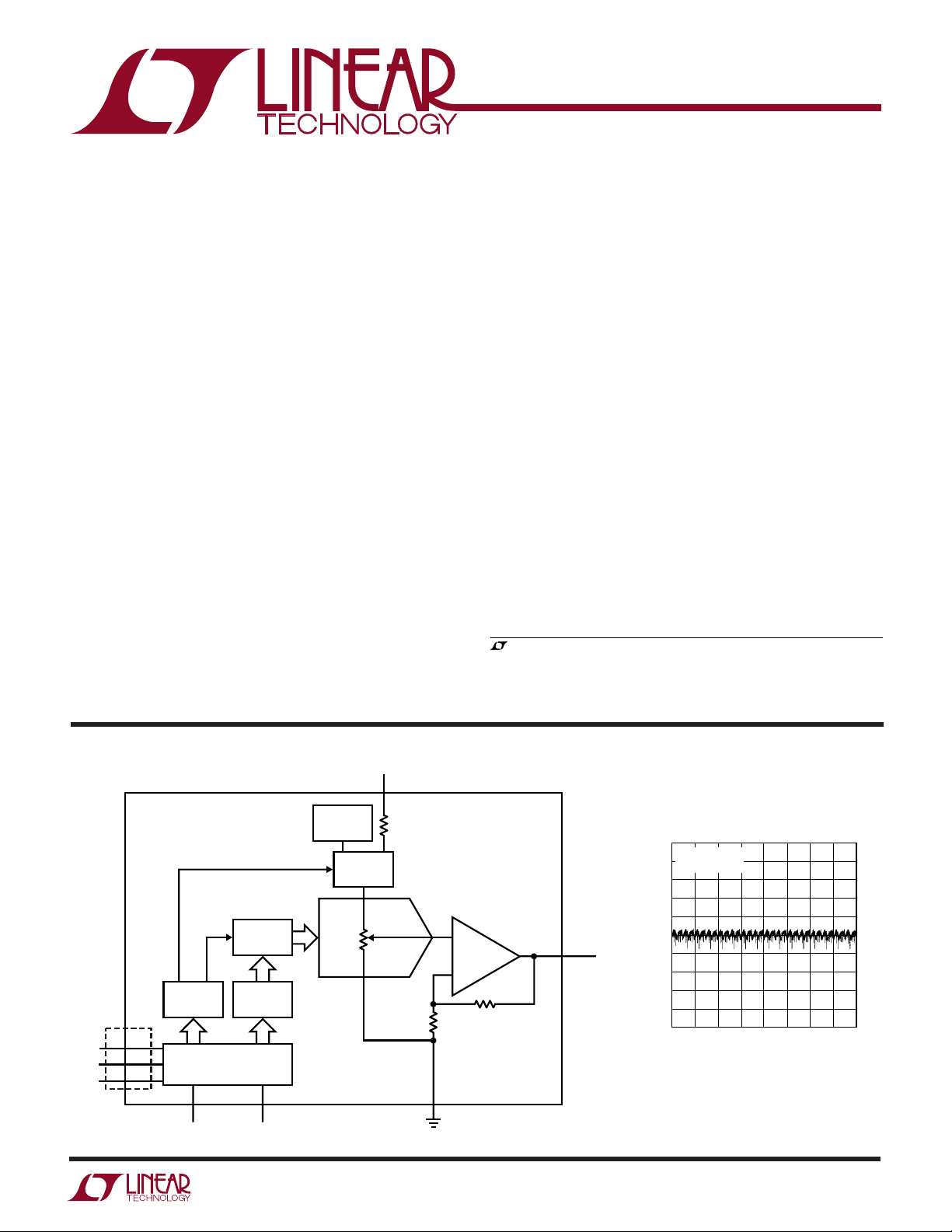
BLOCK DIAGRA
DAC LATCH
AD0
AD1
AD2
COMMAND
LATCH
2-WIRE INTERFACE
SDA
1 (1) 5 (4)
MSOP
PACKAGE
ONLY
(6)
(2)
(3)
NOTE: PIN NUMBERS IN PARENTHESES REFER TO THE MSOP PACKAGE
10-BIT
INPUT
LATCH
SCL
W
1.25V
BANDGAP
REFERENCE
REFERENCE
SELECT
4 (5)
V
CC
R
GND
2 (7)
Differential Nonlinearity (DNL)
1.0
V
= VCC = 5V
REF
0.8
= 25°C
T
A
0.6
0.4
0.2
+
–
R
V
OUT
1663 BD
3 (8)
0
–0.2
ERROR (LSB)
–0.4
–0.6
–0.8
–1.0
0
28 384
156
512
CODE
640
768
896
1024
1663 G02
1
Page 2
LTC1663
A
W
O
LUTEXI TIS
S
A
WUW
U
ARB
G
(Note 1)
VCC to GND .............................................. –0.3V to 7.5V
SDA, SCL ..................................................–0.3V to 7.5V
AD0, AD1, AD2 (MSOP Only) ...... – 0.3V to (VCC + 0.3V)
V
............................................ –0.3V to (VCC + 0.3V)
OUT
WU
/
PACKAGE
SDA
AD1
AD2
SCL
8-LEAD PLASTIC MSOP
T
JMAX
Consult factory for Military grade parts.
LECTRICAL C CHARA TERIST
E
temperature range, otherwise specifications are at T
unless otherwise noted.
O
RDER I FOR ATIO
TOP VIEW
1
2
3
4
MS8 PACKAGE
= 125°C, θJA = 150°C/W
ORDER PART
NUMBER
8
V
OUT
7
GND
6
AD0
5
V
CC
LTC1663CMS8
LTC1663IMS8
MS8 PART MARKING
LTEQ
LTJJ
ICS
The ● denotes specifications which apply over the full operating
= 25°C. V
A
Operating Temperature Range
LTC1663C .............................................. 0°C to 70°C
LTC1663I........................................... –40°C to 85°C
Storage Temperature Range ................ –65°C to 150°C
Lead Temperature (Soldering, 10 sec)................. 300°C
U
ORDER PART
NUMBER
LTC1663CS5
S5 PART MARKING
LTEP
unloaded,
SDA 1
GND 2
V
OUT
T
JMAX
= 2.7V to 5.5V, V
CC
TOP VIEW
3
S5 PACKAGE
5-LEAD PLASTIC SOT-23
= 125°C, θJA = 250°C/W
set as reference, V
CC
5 SCL
4 V
CC
OUT
SYMBOL PARAMETER CONDITIONS MIN TYP MAX UNITS
DAC
Resolution ● 10 Bits
Monotonicity (Note 2) ● 10 Bits
DNL Differential Nonlinearity Guaranteed Monotonic (Note 2) ● ±0.2 ±0.75 LSB
INL Integral Nonlinearity (Note 2) ● ±0.5 ±2.5 LSB
V
OS
V
OSTC
FSE Full-Scale Error Reference Set to V
V
OUT
V
FSTC
PSRR Power Supply Rejection Ratio Reference Set to Internal Bandgap, ±0.4 LSB/V
Power Supply
V
CC
I
CC
I
SD
Op Amp DC Performance
Offset Error Measured at Code 20 ● ±10 ±30 mV
Offset Error Temperature Coefficient ±15 µV/°C
Reference Set to Internal Bandgap
DAC Output Span Reference Set to V
Full-Scale Voltage Temperature Coefficient ±30 µV/°C
Positive Supply Voltage ● 2.7 5.5 V
Supply Current VCC = 3V (Note 3) ● 60 100 µA
Supply Current in Shutdown Mode (Note 3) ● 10 16 µA
Short-Circuit Current (Sourcing) V
Short-Circuit Current (Sinking) V
Output Impedance to GND Input Code = 0, VCC = 5V 65 Ω
Reference Set to Internal Bandgap 0 to 2.5 V
Code = 1023
VCC = 5V (Note 3) ● 75 125 µA
Shorted to GND, Input Code = 1023 ● 25 100 mA
OUT
Shorted to VCC, Input Code = 0 ● 30 120 mA
OUT
Input Code = 0, V
In Shutdown Mode 500 kΩ
CC
CC
= 3V 150 Ω
CC
● ±3 ±15 LSB
● ±3 ±15 LSB
0 to V
CC
V
2
Page 3

LTC1663
LECTRICAL C CHARA TERIST
E
ICS
temperature range, otherwise specifications are at T
The ● denotes specifications which apply over the full operating
= 25°C. V
A
= 2.7V to 5.5V, V
CC
set as reference, V
CC
unloaded,
OUT
unless otherwise noted.
SYMBOL PARAMETER CONDITIONS MIN TYP MAX UNITS
Output Impedance to V
AC Performance
Voltage Output Slew Rate Rising (Notes 4, 5) 0.75 V/µs
Voltage Output Settling Time To ±0.5LSB (Notes 4, 5) 30 µs
Digital Feedthrough 0.75 nV • s
Digital-to-Analog Glitch Impulse 1LSB Change Around Major Carry 70 nV • s
Digital Inputs SCL, SDA
V
IH
V
IL
V
LTH
I
LEAK
C
IN
Digital Output SDA
V
OL
Address Inputs AD0, AD1, AD2 (MSOP Only)
I
UP
V
IH
V
IL
High Level Input Voltage ● 1.4 V
Low Level Input Voltage ● 0.6 V
Logic Threshold Voltage 1V
Digital Input Leakage VCC = 5.5V and 0V, VIN = GND to V
Digital Input Capacitance (Note 7) ● 10 pF
Digital Output Low Voltage I
Address Pin Pull-Up Current VIN = 0V ● 0.5 1.5 µA
High Level Input Voltage ● VCC – 0.3 V
Low Level Input Voltage ● 0.8 V
CC
Input Code = 1023, VCC = 5V 80 Ω
Input Code = 1023, V
Falling (Notes 4, 5) 0.25 V/µs
= 350µA ● 0.4 V
PULLUP
= 3V 120 Ω
CC
CC
● ±1 µA
UW
TI I G CHARACTERISTICS
range, otherwise specifications are at T
SYMBOL PARAMETER MIN TYP MAX UNITS
SMBus Timing Characteristics (Notes 6, 7)
f
SMB
t
BUF
t
HD, STA
t
SU, STA
t
SU, STO
t
HD, DAT
t
SU, DAT
t
LOW
t
HIGH
t
f
t
r
Note 1: Absolute maximum ratings are those values beyond which the life
of a device may be impaired.
Note 2: Nonlinearity and monotonicity are defined from code 20 to code
1003 (full scale). See Applications Information.
Note 3: Digital inputs at 0V or V
SMBus Operating Frequency ● 10 100 kHz
Bus Free Time Between Stop and Start Condition ● 4.7 µs
Hold Time After (Repeated) Start Condition ● 4.0 µs
Repeated Start Condition Setup Time ● 4.7 µs
Stop Condition Setup Time ● 4.0 µs
Data Hold Time ● 300 ns
Data Setup Time ● 250 ns
Clock Low Period ● 4.7 µs
Clock High Period ● 4.0 50 µs
Clock, Data Fall Time ● 300 ns
Clock, Data Rise Time ● 1000 ns
.
CC
= 25°C. V
A
The ● denotes specifications which apply over the full operating temperature
= 2.7V to 5.5V, V
CC
set as reference, V
CC
Note 4: Load is 10kΩ in parallel with 100pF.
= V
Note 5: V
i.e., codes k = 102 and k = 922.
Note 6: All values are referenced to V
Note 7: Guaranteed by design and not subject to test.
CC
= 5V. DAC switched between 0.1VFS and 0.9VFS,
REF
unloaded, unless otherwise noted.
OUT
and VIL levels.
IH
3
Page 4
LTC1663
UW
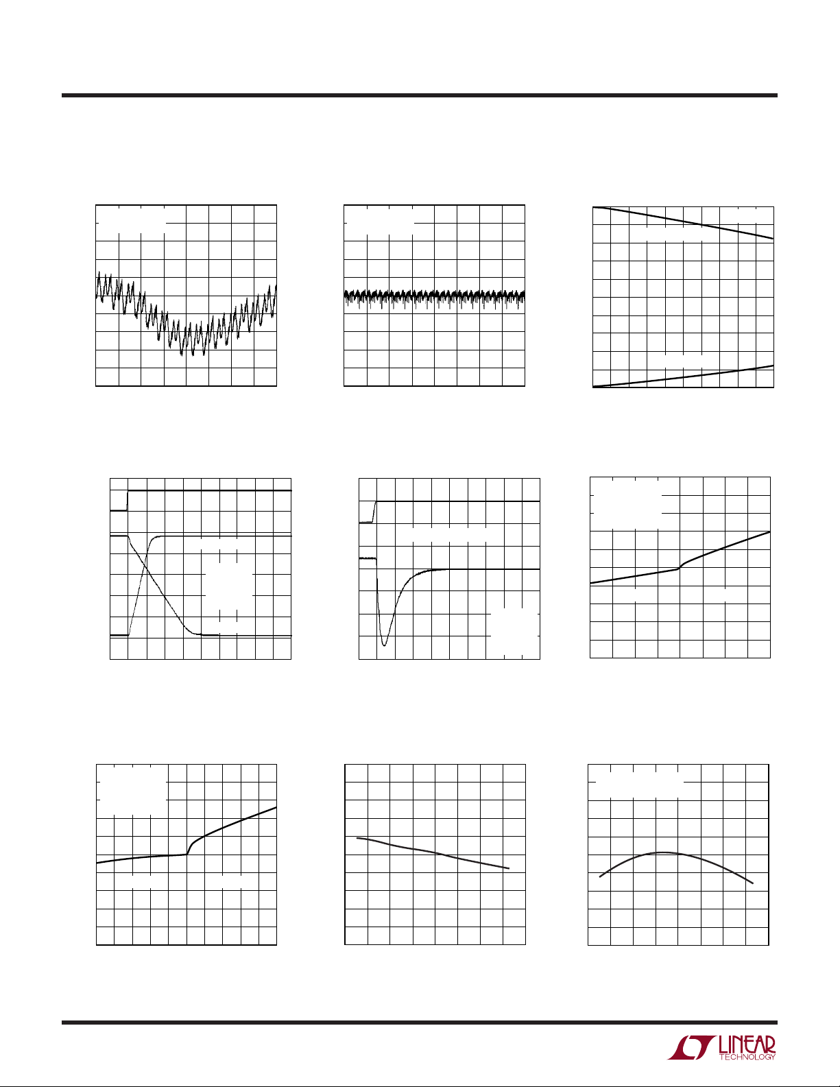
TYPICAL PERFOR A CE CHARACTERISTICS
1.0
V
REF
0.8
T
A
0.6
0.4
0.2
0
–0.2
ERROR (LSB)
–0.4
–0.6
–0.8
–1.0
0
= VCC = 5V
= 25°C
28 384
156
512
CODE
640
768
896
1024
1663 G01
1.0
V
REF
0.8
T
A
0.6
0.4
0.2
0
–0.2
ERROR (LSB)
–0.4
–0.6
–0.8
–1.0
0
= VCC = 5V
= 25°C
28 384
156
512
CODE
640
768
896
1663 G02
1024
Source and Sink Current
Capability with VCC = 5VDifferential Nonlinearity (DNL)Integral Nonlinearity (INL)
5.0
4.5
4.0
3.5
3.0
2.5
2.0
1.5
OUTPUT VOLTAGE (V)
1.0
0.5
0
01 3
DAC CODE = 1023
DAC CODE = 0
2
46579
OUTPUT CURRENT SOURCE/SINK (mA)
TA = 25°C
8
1011 G03
10
Large-Signal Step Response Midscale Glitch
5
SDA
(VOLTS)
0
V
OUT
(VOLTS)
5
4
3
2
1
0
CODE = 990
VCC = 5V
R
C
T
5µs/DIV
CODE = 32
Load Regulation vs Output Current
1.0
0.8
0.6
0.4
0.2
(LSB)
OUT
–0.2
∆V
–0.4
–0.6
–0.8
–1.0
VCC = V
V
CODE = 512
T
0
–1.0
= 3V
REF
= 1.5V
OUT
= 25°C
A
SOURCE SINK
–0.8 – 0.2
–0.6–0.4
I
OUT
0
(mA)
0.2
= 4.7k
L
= 100pF
L
= 25°C
A
Load Regulation vs Output Current
1.0
VCC = V
0.8
5V
SDA
1663 G04
V
OUT
10mV/DIV
0V
CODE = 512 TO 511
2µs/DIV
VCC = 5V
R
= 4.7k
L
= 100pF
C
L
= 25°C
T
A
1663 G05
Offset Error Voltage vs
Temperature
5
4
3
2
1
0
–1
–2
–3
OFFSET ERROR VOLTAGE (mV)
–4
0.8
1.0
0.60.4
1663 G07
–5
–60
–20
–40 0
TEMPERATURE (°C)
20
40
80
60
100
1663 G08
V
CODE = 512
0.6
T
0.4
0.2
(LSB)
0
OUT
–0.2
∆V
–0.4
–0.6
–0.8
–1.0
–4
Full-Scale Output Voltage vs
Temperature
2.510
2.508
2.506
2.504
2.502
2.500
2.498
2.496
OUTPUT VOLTAGE (V)
2.494
2.492
2.490
–60
= 5V
REF
= 2.5V
OUT
= 25°C
A
SOURCE SINK
–3 –1
–2
REFERENCE SET TO
INTERNAL BANDGAP
–20
–40 0
0
I
(mA)
OUT
20
TEMPERATURE (°C)
3
2
1
60
40
80
4
1663 G06
100
1663 G09
4
Page 5

UUU
PIN FUNCTIONS
SDA (Pin 1, Pin 1 on SOT-23): Serial Data Bidirectional
Pin. Data is shifted into the SDA pin and acknowledged by
the SDA pin. High impedance pin while data is shifted in.
Open-drain N-channel output during acknowledgment.
Requires a pull-up resistor or current source to VCC.
AD1 (Pin 2): Slave Address Select Bit 1. Tie this pin to
either VCC or GND to modify the corresponding bit of the
LTC1663’s slave address.
AD2 (Pin 3): Slave Address Select Bit 2. Tie this pin to
either VCC or GND to modify the corresponding bit of the
LTC1663’s slave address.
SCL (Pin 4, Pin 5 on SOT-23): Serial Clock Input Pin. Data
is shifted into the SDA pin at the rising edges of the clock.
This high impedance pin requires a pull-up resistor or
current source to VCC.
LTC1663
V
(Pin 5, Pin 4 on SOT-23): Power Supply. 2.7V ≤ V
CC
≤ 5.5V. Also used as the reference voltage input when the
part is programmed to use VCC as the reference.
AD0 (Pin 6): Slave Address Select Bit 0. Tie this pin to
either VCC or GND to modify the corresponding bit of the
LTC1663’s slave address.
GND (Pin 7, Pin 2 on SOT-23): System Ground.
V
(Pin 8, Pin 3 on SOT-23): Voltage Output. Buffered
OUT
rail-to-rail DAC output.
CC
UU
DEFINITIONS
Differential Nonlinearity (DNL): The difference between
the measured change and the ideal 1LSB change for any
two adjacent codes. The DNL error between any two codes
is calculated as follows:
DNL = (∆V
Where ∆V
two adjacent codes.
Digital Feedthrough: The glitch that appears at the analog
output caused by AC coupling from the digital inputs when
they change state. The area of the glitch is specified in
(nV)(sec).
Full-Scale Error (FSE): The deviation of the actual fullscale voltage from ideal. FSE includes the effects of offset
and gain errors (see Applications Information).
Integral Nonlinearity (INL): The deviation from a straight
line passing through the endpoints of the DAC transfer
curve (Endpoint INL). Because the output cannot go below
zero, the linearity is measured between full scale and the
lowest code that guarantees the output will be greater than
OUT
– LSB)/LSB
OUT
is the measured voltage difference between
zero. The INL error at a given input code is
follows:
INL = [V
Where V
the given input code.
Least Significant Bit (LSB): The ideal voltage difference
between two successive codes.
LSB = V
Resolution (n): Defines the number of DAC output states
(2n) that divide the full-scale range. Resolution does not
imply linearity.
Voltage Offset Error (VOS): Nominally, the voltage at the
output when the DAC is loaded with all zeros. A single
supply DAC can have a true negative offset, but the output
cannot go below zero (see Applications Information).
For this reason, single supply DAC offset is measured at
the lowest code that guarantees the output will be greater
than zero.
– VOS – (VFS – VOS)(code/1023)]/LSB
OUT
is the output voltage of the DAC measured at
OUT
/1024
REF
calculated as
5
Page 6

ACK ACK
123
ADDRESS
456789123456789123456789123456789
FULL-SCALE
VOLTAGE
ZERO-SCALE
VOLTAGE
1663 TA02
01001110 XXXXX000 11111111 XXXXXX11ACK
STOPSTART
SDA
SCL
V
OUT
NOTE: X = DON’T CARE
ACK
COMMAND LS DATA MS DATA
LTC1663
UWW
TI I G DIAGRA
t
BUF
SU, STO
t
1663 TD
START
CONDITION
STOP
CONDITION
SDA
t
SU, STA
t
t
SU, DAT
t
t
HD, STA
HD, DAT
LOW
SCL
HIGH
t
HD, STA
t
CONDITION
REPEATED START
f
t
r
t
START
CONDITION
Typical Input Waveform—Programming DAC Output for Full Scale (AD2 to AD0 Set High)
6
Page 7

LTC1663
U
WUU
APPLICATIONS INFORMATION
Write Word Protocol Used by the LTC1663
81711818
Command Byte ASlave Address AWr LSData Byte A MSData Byte A PS
S = Start Condition, Wr = Write Bit = 0, A = Acknowledge, P = Stop Condition
Serial Digital Interface
The LTC1663 communicates with a host (master) using
the standard 2-wire interface. The Timing Diagram shows
the timing relationship of the signals on the bus. The two
bus lines, SDA and SCL, must be high when the bus is not
in use. External pull-up resistors or current sources, such
as the LTC1694 SMBus Accelerator, are required on these
lines.
The LTC1663 is a receive-only (slave) device. The master
can communicate with the LTC1663 using the Quick
Command, Send Byte or Write Word protocols as explained later.
The START and STOP Conditions
When the bus is not in use, both SCL and SDA must be
high. A bus master signals the beginning of a communication to a slave device by transmitting a START condition.
A START condition is generated by transitioning SDA
from high to low while SCL is high.
When the master has finished communicating with the
slave, it issues a STOP condition. A STOP condition is
generated by transitioning SDA from low to high while SCL
is high. The bus is then free for communication with
another SMBus device.
Acknowledge
The Acknowledge signal is used for handshaking between
the master and the slave. An Acknowledge (active LOW)
generated by the slave lets the master know that the latest
byte of information was received. The Acknowledge related clock pulse is generated by the master. The master
releases the SDA line (HIGH) during the Acknowledge
clock pulse. The slave-receiver must pull down the SDA
line during the Acknowledge clock pulse so that it remains
a stable LOW during the HIGH period of this clock pulse.
111
1663 TA03
Write Word Protocol
The master initiates communication with the LTC1663
with a START condition and a 7-bit address followed by the
Write Bit (Wr) = 0. The LTC1663 acknowledges and the
master delivers the command byte. The LTC1663 acknowledges and latches the command byte into the command byte input register. The master then delivers the
least significant data byte. Again the LTC1663 acknowledges and the data is latched into the least significant data
byte input register. The master then delivers the most
significant data byte. The LTC1663 acknowledges once
more and latches the data into the most significant data
byte input register. Lastly, the master terminates the
communication with a STOP condition. On the reception
of the STOP condition, the LTC1663 transfers the input
register information to output registers and the DAC
output is updated.
Slave Address (MSOP Package Only)
The LTC1663 can respond to one of eight 7-bit addresses.
The first 4 bits (MSBs) have been factory programmed to
0100. The three address bits, AD2, AD1 and AD0 are
programmed by the user and determine the LSBs of the
slave address, as shown in the table below:
AD2 AD1 AD0 0100 xxx
L L L 0100 000
L L H 0100 001
L H L 0100 010
L H H 0100 011
H L L 0100 100
H L H 0100 101
H H L 0100 110
H H H 0100 111
7
Page 8

LTC1663
Command Byte ASlave Address AWr PS
811711
1663 TA04
1
S = Start Condition, Wr = Write Bit, A = Acknowledge, P = Stop Condition
U
WUU
APPLICATIONS INFORMATION
Slave Address (SOT-23 Package)
The slave address for the SOT-23 package has been
factory programmed to be “0100 000.” If another address
is required, please consult the factory.
Command Byte
76543210
XXXXXBGSDSY
SY 1 Allows update on Acknowledge of SYNC Address only
0 Update on Stop condition only (Power-On Default)
SD 1 Puts the device in power-down mode
0 Puts the device in standard operating mode
(Power-On Default)
BG 1 Selects the internal bandgap reference
0 Selects the supply as the reference (Power-On Default)
X X Don’t Care
The stop condition normally initiates the update of the
DAC’s output latches. This allows for simultaneous update
of more than one DAC or other devices on the bus. This can
be overridden by setting the “SY” bit of the command byte.
Setting this bit sets the device to update the DAC output
latches at the reception of a SYNC address quick command. The actual update occurs on the rising edge of SCL
during the Acknowledge. In this way, all devices can
update on the reception of the SYNC address quick command instead of the STOP condition.
A Shutdown (SD) bit = HIGH will put the device in a low
power state but retain all data latch information. Shutdown
will occur at the reception of a STOP condition. This way
shutdown could be synchronized to other devices. The
output impedance of the DAC will go to a high impedance
state (≈500kΩ to GND).
The Bandgap (BG) bit when set to “0” selects the DAC
supply voltage as its voltage reference. The full-scale
output of the DAC with this setting is equal to the supply
voltage. When the BG bit is set to “1,” the internal bandgap
reference (≈1.25V) is selected as the DAC’s reference. The
full-scale output voltage for this setting is 2.5V.
Data Bytes
Least Significant Data Byte
7654321 0
D7 D6 D5 D4 D3 D2 D1 D0
Most Significant Data Byte
76543210
X X X X X X D9 D8
X = Don’t care
Send Byte Protocol
The Send Byte protocol used on the LTC1663 is actually a
subset of the Write Word protocol described previously.
The Send Byte protocol can only be used to send the
command byte information to the LTC1663.
The Send Byte protocol is also used whenever the Write
Word protocol is interrupted for any reason. Reception of
a START or STOP condition after the Acknowledge of the
command byte, but before the Acknowledge of the last
data byte, will cause both data bytes to be ignored and the
command byte to be accepted.
Reception of a START or STOP condition before the
Acknowledge of the command byte will cause the interrupted command byte to be ignored.
8
Page 9

LTC1663
U
WUU
APPLICATIONS INFORMATION
SYNC Address/Quick Command
In addition to the slave address, the LTC1663 has an
address that can be shared by other devices so that they
may be updated synchronously. The address is called to
the SYNC address and uses the quick command protocol.
The SYNC Address is 1111 110
1
SYNC Address
SY/CLR 1 Update output latches on rising edge of SCL during
Acknowledge of SYNC Address
0 Clear all internal latches on rising edge of SCL during
Acknowledge of SYNC Address
The SY/CLR bit set high only has meaning when the “SY”
bit of the command byte was previously set HIGH. On the
otherhand, the SY/CLR bit set LOW will always clear the
part, independent of the state of the “SY” bit in the
command byte.
Input Threshold
1171
Ack StopStart 1111 110 SY/CLR
1663 TA05
A small resistor placed in series with the output can be
used to achieve stability for any load capacitance greater
than 1000pF. For example, a 0.1µF load can be driven by
the LTC1663 if a 110Ω series resistance is used. The phase
margin of the resulting circuit is 45° and increases monotonically from this point if larger values of resistance, capacitance or both are substituted for the values given.
Rail-to-Rail Output Considerations
As in any rail-to-rail device, the output is limited to
voltages within the supply range.
If the DAC offset is negative, the output for the lowest
codes limits at 0V as shown in Figure 1b.
Similarly, limiting can occur near full scale when VCC is
used as the reference. If V
= VCC and the DAC full-scale
REF
error (FSE) is positive, the output for the highest codes
limits at VCC as shown in Figure 1c. No full-scale limiting
can occur if the internal reference is used.
Offset and linearity are defined and tested over the region
of the DAC transfer function where no output limiting can
occur.
Anticipating the trend toward lower supply voltages, the
SMBus is specified with a VIH of 1.4V and a VIL of 0.6V.
While some SMBus parts may violate this stringent SMBus
specification by allowing a higher VIH value for a correspondingly higher input supply voltage, the LTC1663
meets and maintains the constant SMBus input threshold
specification across the entire supply voltage range of
2.7V to 5.5V. The logic input threshold is designed to be
1V with 50mV of hysteresis.
Voltage Output
The output amplifier contained in the LTC1663 can source
or sink up to 5mA. The output stage swings to within a few
millivolts of either supply rail when unloaded and has an
equivalent output resistance of 85Ω when driving a load to
the rails. The output amplifier is stable driving capacitive
loads up to 1000pF.
Internal Reference
In applications where a predictable output is required that
is independent of supply voltage, the LTC1663 has a userselectable internal reference. Selecting the internal reference will set the full-scale output voltage to 2.5V. This can
be useful in applications where the supply voltage is
poorly regulated.
Using the LT®1460 Micropower Series Reference as a
Power Supply for the LTC1663
In applications where the advantages of using the internal
reference are required but the full-scale range needs to be
greater than 2.5V, an external series reference can be
used. The LT1460 is ideal for use as a power supply for the
LTC1663 and can provide 3V, 3.3V and 5V full-scale
output voltage ranges. The LT1460 provides accuracy,
noise immunity and extended supply range to the LTC1663
when the LTC1663 is operated ratiometric to VCC. Since
both parts are available in SOT-23 packages, the PC board
space for this application is extremely small. See Figure 2.
9
Page 10

LTC1663
U
WUU
APPLICATIONS INFORMATION
OUTPUT
VOLTAGE
OUTPUT
VOLTAGE
= V
V
REF
CC
5120 1023
INPUT CODE
(a)
V
= V
REF
INPUT CODE
(c)
POSITIVE
CC
FSE
OUTPUT
VOLTAGE
OFFSET
0V
INPUT CODE
(b)
NEGATIVE
Figure 1. Effects of Rail-to-Rail Operation On a DAC Transfer Curve. (a) Overall Transfer Function (b) Effect of Negative
Offset for Codes Near Zero Scale (c) Effect of Positive Full-Scale Error for Input Codes Near Full Scale When V
3.9V TO 20V
LT1460S3-3
1
IN
0.1µF
REFER TO MSOP PACKAGE
GND
2
OUT
+
3
TO
µP
0.01µF
5 (4)
1 (1)
SCL
SDA
3V
V
GND
CC
4 (5)
2 (7)LTC1663 PIN NUMBERS IN PARENTHESES
3 (8)
OUTLTC1663 0V ≤ V
OUT
≤ 3V
1663 F02
REF
Figure 2. LT1460 As Power Supply for the LTC1663
= V
1663 F01
CC
10
Page 11

PACKAGE DESCRIPTION
0.007
(0.18)
0.021
± 0.006
(0.53 ± 0.015)
* DIMENSION DOES NOT INCLUDE MOLD FLASH, PROTRUSIONS OR GATE BURRS. MOLD FLASH,
PROTRUSIONS OR GATE BURRS SHALL NOT EXCEED 0.006" (0.152mm) PER SIDE
** DIMENSION DOES NOT INCLUDE INTERLEAD FLASH OR PROTRUSIONS.
INTERLEAD FLASH OR PROTRUSIONS SHALL NOT EXCEED 0.006" (0.152mm) PER SIDE
° – 6° TYP
0
U
Dimensions in inches (millimeters) unless otherwise noted.
MS8 Package
8-Lead Plastic MSOP
(LTC DWG # 05-08-1660)
0.118 ± 0.004*
(3.00 ± 0.102)
0.193 ± 0.006
(4.90 ± 0.15)
SEATING
PLANE
0.040
± 0.006
(1.02 ± 0.15)
0.012
(0.30)
0.0256
REF
0.034 ± 0.004
(0.86 ± 0.102)
0.006 ± 0.004
(0.15 ± 0.102)
(0.65)
BSC
8
7
12
LTC1663
6
5
0.118 ± 0.004**
(3.00 ± 0.102)
MSOP (MS8) 1098
4
3
S5 Package
5-Lead Plastic SOT-23
(LTC DWG # 05-08-1633)
2.80 – 3.00
(0.110 – 0.118)
(NOTE 3)
1.90
2.60 – 3.00
(0.102 – 0.118)
1.50 – 1.75
(0.059 – 0.069)
0.35 – 0.55
(0.014 – 0.022)
NOTE:
1. DIMENSIONS ARE IN MILLIMETERS
2. DIMENSIONS ARE INCLUSIVE OF PLATING
3. DIMENSIONS ARE EXCLUSIVE OF MOLD FLASH AND METAL BURR
4. MOLD FLASH SHALL NOT EXCEED 0.254mm
5. PACKAGE EIAJ REFERENCE IS SC-74A (EIAJ)
0.09 – 0.20
(0.004 – 0.008)
(NOTE 2)
(0.074)
REF
0.00 – 0.15
(0.00 – 0.006)
0.35 – 0.50
(0.014 – 0.020)
FIVE PLACES (NOTE 2)
0.95
(0.037)
REF
0.90 – 1.45
(0.035 – 0.057)
0.90 – 1.30
(0.035 – 0.051)
S5 SOT-23 0599
Information furnished by Linear Technology Corporation is believed to be accurate and reliable.
However, no responsibility is assumed for its use. Linear Technology Corporation makes no representation that the interconnection of its circuits as described herein will not infringe on existing patent rights.
11
Page 12

LTC1663
TYPICAL APPLICATION
Program Up to 8 Control Outputs Per BUS and Place Them Where They Are Needed
U
VCC = 2.7V TO 5.5V
5
4
SMBus 1
LTC1694
SMBus 2
GND
1
V
CC
+
0.1µF
2
SCL
µP
SDA
TO OTHER SMBus
DEVICES
4
1
6
2
3
4
1
6
2
3
4
1
6
2
3
SCL
SDA
LTC1663CMS8
AD0
AD1
AD2
SCL
SDA
LTC1663CMS8
AD0
AD1
AD2
SCL
SDA
LTC1663CMS8
AD0
AD1
AD2
V
GND
V
GND
V
GND
5
CC
7
5
CC
7
5
CC
7
+
0.1µF
8
V
OUT
CONTROL
OUTPUT 0
0V ≤ V
OUT0
< V
CC
+
0.1µF
8
V
OUT
CONTROL
OUTPUT 1
0V ≤ V
OUT1
< V
CC
+
0.1µF
8
V
OUT
CONTROL
OUTPUT 7
0V ≤ V
OUT7
1663 TA06
< V
CC
RELATED PARTS
PART NUMBER DESCRIPTION COMMENTS
LTC1694 SMBus I2C Accelerator Dual SMBus Accelerator with Active AC and DC Pull-Up Current Sources
LTC1694-1 SMBus I2C Accelerator Dual SMBus Accelerator with Active AC Pull-Up Current Only
DACs
LTC1659 Single Rail-to-Rail 12-Bit V
8-Lead MSOP Package. V
LTC1660/LTC1664 Octal/Quad 10-Bit V
LTC1661 Dual 10-Bit V
OUT
in 8-Lead MSOP Package VCC = 2.7V to 5.5V Micropower Rail-to-Rail Output. 3-Wire Interface.
OUT
ADCs
LTC1285/LTC1288 8-Pin SO, 3V Micropower ADCs 1- or 2-Channel, Autoshutdown
LTC1286/LTC1298 8-Pin SO, 5V Micropower ADCs 1- or 2-Channel, Autoshutdown
LTC1594/LTC1598 4/8-Channel, 5V Micropower 12-Bit ADCs Low Power, Small Size, Low Cost
Linear Technology Corporation
12
1630 McCarthy Blvd., Milpitas, CA 95035-7417
(408) 432-1900 ● FAX: (408) 434-0507
DAC in Low Power Multiplying V
OUT
= 2.7V to 5.5V GND to REF. REF Input Can Be Tied to VCC. 3-Wire Interface.
CC
DAC. Output Swings from
OUT
DACs in 16-Pin Narrow SSOP VCC = 2.7V to 5.5V Micropower Rail-to-Rail Output. 3-Wire Interface.
1663f LT/TP 0300 4K • PRINTED IN THE USA
●
www.linear-tech.com
LINEAR TECHNOLOGY CORPORATION 1999
 Loading...