

Page 1
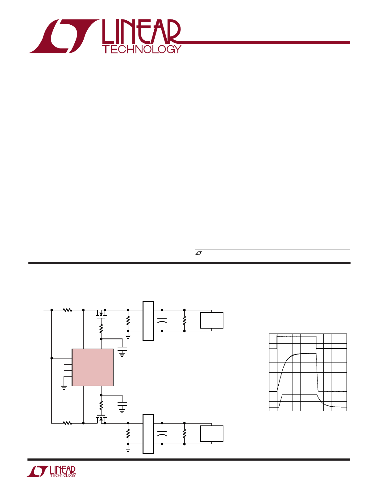
5ms/DIV
2.5V/DIV
1647-1/2/3 TA01a
V
ON
V
GATE
V
OUT
FEATURES
LTC1647-1/LTC1647-2/LTC1647-3
Dual Hot Swap Controllers
U
DESCRIPTIO
■
Allows Safe Board Insertion and Removal from a
Live Backplane
■
Programmable Electronic Circuit Breaker
■
FAULT Output Indication
■
Programmable Supply Voltage Power-Up Rate
■
High Side Drive for External MOSFET Switches
■
Controls Supply Voltages from 2.7V to 16.5V
■
Undervoltage Lockout
U
APPLICATIO S
■
Hot Board Insertion
■
Electronic Circuit Breaker
■
Portable Computer Device Bays
■
Hot Plug Disk Drive
The LTC®1647-1/LTC1647-2/LTC1647-3 are dual Hot
SwapTM controllers that permit a board to be safely inserted and removed from a live backplane.
Using external N-channel MOSFETs, the board supply
voltages can be ramped up at a programmable rate. A high
side switch driver controls the MOSFET gates for supply
voltages ranging from 2.7V to 16.5V. A programmable
electronic circuit breaker protects against overloads and
shorts. The ON pins are used to control board power or
clear a fault.
The LTC1647-1 is a dual Hot Swap controller with a
common VCC pin, separate ON pins and is available in an
SO-8 package. The LTC1647-2 is similar to the LTC1647-1
but combines a fault status flag with automatic retry at the
ON pins and is also available in the SO-8 package. The
LTC1647-3 has individual VCC pins, ON pins and FAULT
status pins for each channel and is available in a 16-lead
narrow SSOP package.
, LTC and LT are registered trademarks of Linear Technology Corporation.
Hot Swap is a trademark of Linear Technology Corporation.
TYPICAL APPLICATIO
3.3V V
SUPPLY
R1
ON1
ON2
0.1Ω
R5
0.1Ω
1
2
3
4
SENSE 1
V
CC
ON1
ON2
GND
SENSE 2
ID
Q1
1/2 MMDF3N02HD
R2
10Ω
86
GATE 1
LTC1647-1
GATE 2
75
R6
10Ω
Q2
1/2 MMDF3N02HD
U
VID Controller for Two Device Bays
DEVICE #1
R3** R4**C
C1
4.7nF
*C
** R3, R4, R7 AND R8 ARE OPTIONAL DISCHARGE
C3
4.7nF
R7** R8**C
+
CONNECTOR #1
IS USER-SELECTED BASED
LOAD
ON THE DEVICE REQUIREMENTS
RESISTORS WHEN DEVICES ARE POWERED-OFF
Q1, Q2: ON SEMICONDUCTOR
+
CONNECTOR #2
LOAD
DEVICE #2
LOAD
*
*
1394 PHY
AND/OR
USB PORT
1394 PHY
AND/OR
USB PORT
1647-1/2/3 TA01
ON/OFF Sequence
1
Page 2
LTC1647-1/LTC1647-2/LTC1647-3
WW
W
U
ABSOLUTE AXI U RATI GS
(Note 1)
Supply Voltage (VCC) ............................................... 17V
Input Voltage (SENSE)................. –0.3V to (VCC + 0.3V)
Input Voltage (ON).....................................–0.3V to 17V
Output Voltage (FAULT).............................–0.3V to 17V
Output Voltage (GATE) ......... Internally Limited (Note 3)
UUW
PACKAGE/ORDER I FOR A TIO
TOP VIEW
V
1
CC
ON1
2
ON2
3
GND
4
8-LEAD PLASTIC SO
T
JMAX
8
7
6
5
S8 PACKAGE
= 150°C, θJA = 130°C/W
SENSE 1
SENSE 2
GATE 1
GATE 2
V
ON1/FAULT 1
ON2/FAULT 2
GND
T
1
CC
2
3
4
S8 PACKAGE
8-LEAD PLASTIC SO
= 150°C, θJA = 130°C/W
JMAX
Operating Temperature Range
Commercial .............................................0°C to 70°C
Industrial ............................................ –40°C to 85°C
Storage Temperature Range................. –65°C to 150°C
Lead Temperature (Soldering, 10 sec)..................300°C
1
2
3
4
5
6
7
8
TOP VIEW
16
15
14
13
12
11
10
9
V
SENSE 1
SENSE 2
GATE 1
GATE 2
NC
NC
NC
TOP VIEW
8
7
6
5
SENSE 1
SENSE 2
GATE 1
GATE 2
V
CC1
ON1
FAULT 1
ON2
FAULT 2
NC
NC
GND
CC2
GN PACKAGE
16-LEAD PLASTIC SSOP
T
= 150°C, θJA = 130°C/W
JMAX
ORDER PART NUMBER
LTC1647-1CS8
LTC1647-1IS8
S8 PART MARKING
16471
16471I
ORDER PART NUMBER
LTC1647-2CS8
LTC1647-2IS8
S8 PART MARKING
16472
16472I
ORDER PART NUMBER
LTC1647-3CGN
LTC1647-3IGN
GN PART MARKING
16473
16473I
Consult factory for Military grade parts.
ELECTRICAL CHARACTERISTICS
The ● denotes the specifications which apply over the full operating
temperature range, otherwise specifications are at TA = 25°C. VCC = 5V unless otherwise noted. (Note 2)
SYMBOL PARAMETER CONDITIONS MIN TYP MAX UNITS
V
I
I
V
V
V
I
CC
CC
CCX
LKO
LKH
CB
CP
V
Supply Range Operating Range ● 2.7 16.5 V
CCX
VCC Supply Current (Note 4) ON1, ON2 = V
V
Supply Current (Note 5, LTC1647-3) ONX = V
CCX
V
Undervoltage Lockout Coming Out of UVLO (Rising V
CCX
V
Undervoltage Lockout Hysteresis 210 mV
CCX
Circuit Breaker Trip Voltage VCB = V
V
CC1
= 5V, V
CCX
GATE X Output Current ONX High, FAULT X High, V
ONX Low, FAULT X High, V
ONX High, FAULT X Low, V
= V
, ICC = I
CC2
Individually Measured, ● 0.5 5 mA
= 12V or V
SENSEX
CCX
, I
CC2
– V
CC1
CCX
+ I
CC1
CC2
= 12V, V
CC1
CCX
= GND (Sourcing) ● 61014 µA
GATE
= VCC (Sinking) 50 µA
GATE
= 15V (Sinking) 50 mA
GATE
= 5V
CC2
) ● 2.30 2.45 2.60 V
● 1.0 6 mA
● 40 50 60 mV
2
Page 3
LTC1647-1/LTC1647-2/LTC1647-3
ELECTRICAL CHARACTERISTICS
The ● denotes the specifications which apply over the full operating
temperature range, otherwise specifications are at TA = 25°C. VCC = 5V unless otherwise noted. (Note 2)
SYMBOL PARAMETER CONDITIONS MIN TYP MAX UNITS
∆V
V
ONHI
V
ONLO
V
ONHYST
I
IN
V
OL
I
LEAK
t
FAULT
t
RESET
t
ON
t
OFF
Note 1: Absolute Maximum Ratings are those values beyond which the life
of a device may be impaired.
Note 2: All currents into device pins are positive; all currents out of device
pins are negative. All voltages are referenced to ground unless otherwise
specified.
Note 3: An internal Zener on the GATE pins clamp the charge pump
voltage to a typical maximum operating voltage of 28V. External overdrive
of the GATE pin beyond the internal Zener voltage may damage the device.
External MOSFET Gate Drive (V
GATE
(V
GATE
GATE
– VCC), V
– VCC), V
CC1
CC1
= V
= 5V ● 10 13 17 V
CC2
= V
= 12V ● 10 15 19 V
CC2
ONX Threshold High ● 1.20 1.29 1.38 V
ONX Threshold Low ● 1.17 1.21 1.25 V
ONX Hysteresis 70 mV
ONX Input Current ON = GND or V
CC
● ±1 ±10 µA
FAULT X Output Low Voltage IO = 1mA, VCC = 5V ● 0.4 V
(LTC1647-2, LTC1647-3) I
= 5mA, VCC = 5V 0.8 V
O
FAULT X Output Leakage Current No Fault, FAULT X = VCC = 5V ±1 ±10 µA
(LTC1647-3)
Circuit Breaker Delay Time V
CCX
– V
= 0 to 100mV 0.3 µs
SENSEX
Circuit Breaker Reset Time ONX High to Low, to FAULT X High ● 50 100 µs
Turn-On Time ONX Low to High, to GATE X On 2 µs
Turn-Off Time ONX High to Low, to GATE X Off 1 µs
The GATE capacitance must be <0.15µF at maximum V
CC
pin clamp voltage is desired, use an external Zener diode.
Note 4: The total supply current I
is measured with V
CC
CC1
connected internally (LTC1647-1, LTC1647-2) or externally (LTC1647-3).
Note 5: The individual supply current I
The lower of the two supplies, V
CC1
is measured on the LTC1647-3.
CCX
and V
, will have its channel’s
CC2
current. The higher supply will carry the additional supply current of the
charge pump and the bias generator beside its channel’s current.
. If a lower GATE
and V
CC2
PIUTABLES
LTC1647-1 Pinout
PIN DESCRIPTION
1V
CC
2 ON1
3 ON2
4 GND
LTC1647-1 does not have the FAULT status feature.
LTC1647-2 Pinout
PIN DESCRIPTION
1V
CC
2 ON1 and FAULT 1
(Internally Tied Together)
3 ON2 and FAULT 2
(Internally Tied Together)
4 GND
The ONX/FAULT X must be connected to a driver via a resistor if the
autoretry feature is being used..
PIN DESCRIPTION
5 GATE 2
6 GATE 1
7 SENSE 2
8 SENSE 1
PIN DESCRIPTION
5 GATE 2
6 GATE 1
7 SENSE 2
8 SENSE 1
LTC1647-3 Pinout
PIN DESCRIPTION
1V
CC1
2 ON1
3 FAULT 1
4 ON2
5 FAULT 2
6NC
7NC
8 GND
PIN DESCRIPTION
9NC
10 NC
11 NC
12 GATE 2
13 GATE 1
14 SENSE 2
15 SENSE 1
16 V
CC2
3
Page 4

LTC1647-1/LTC1647-2/LTC1647-3
UW
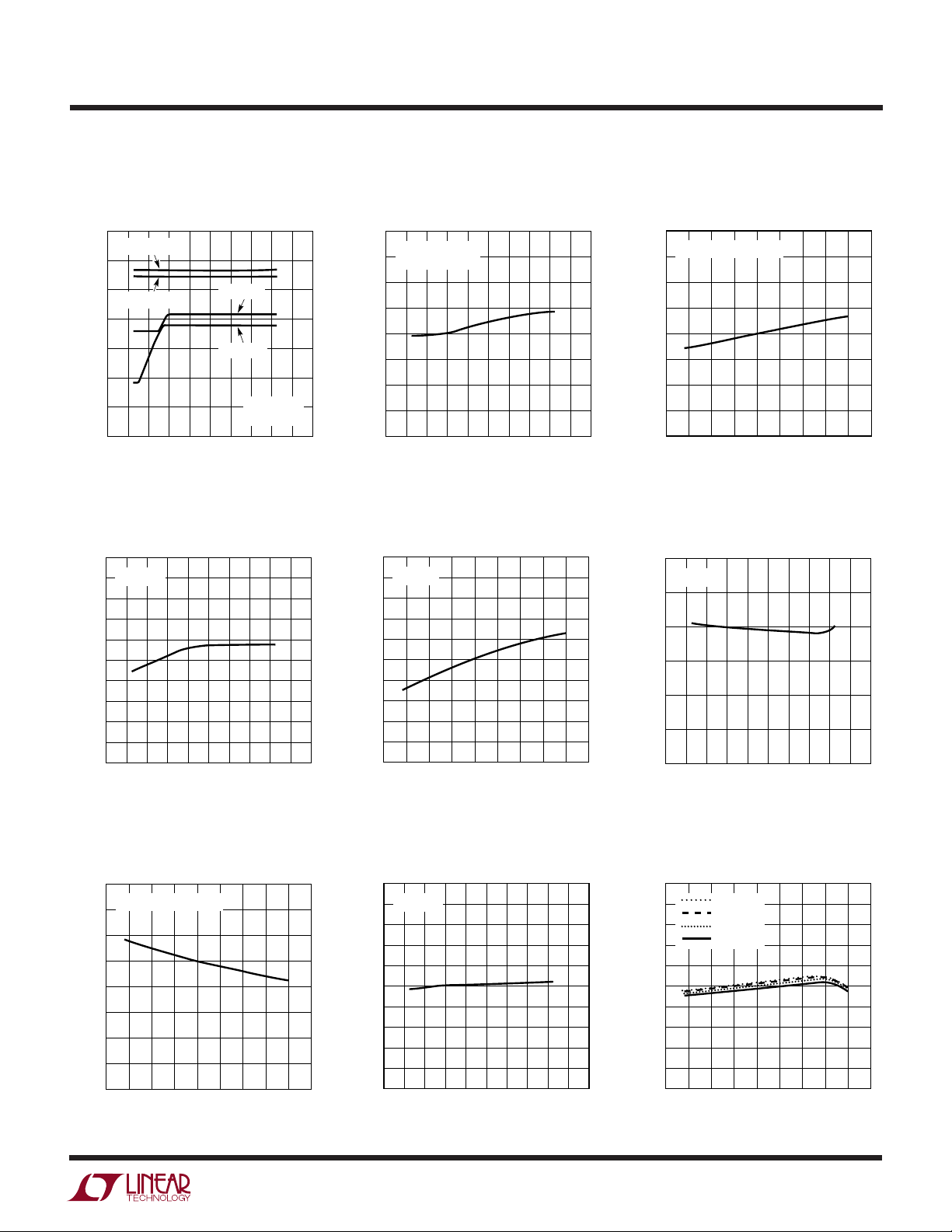
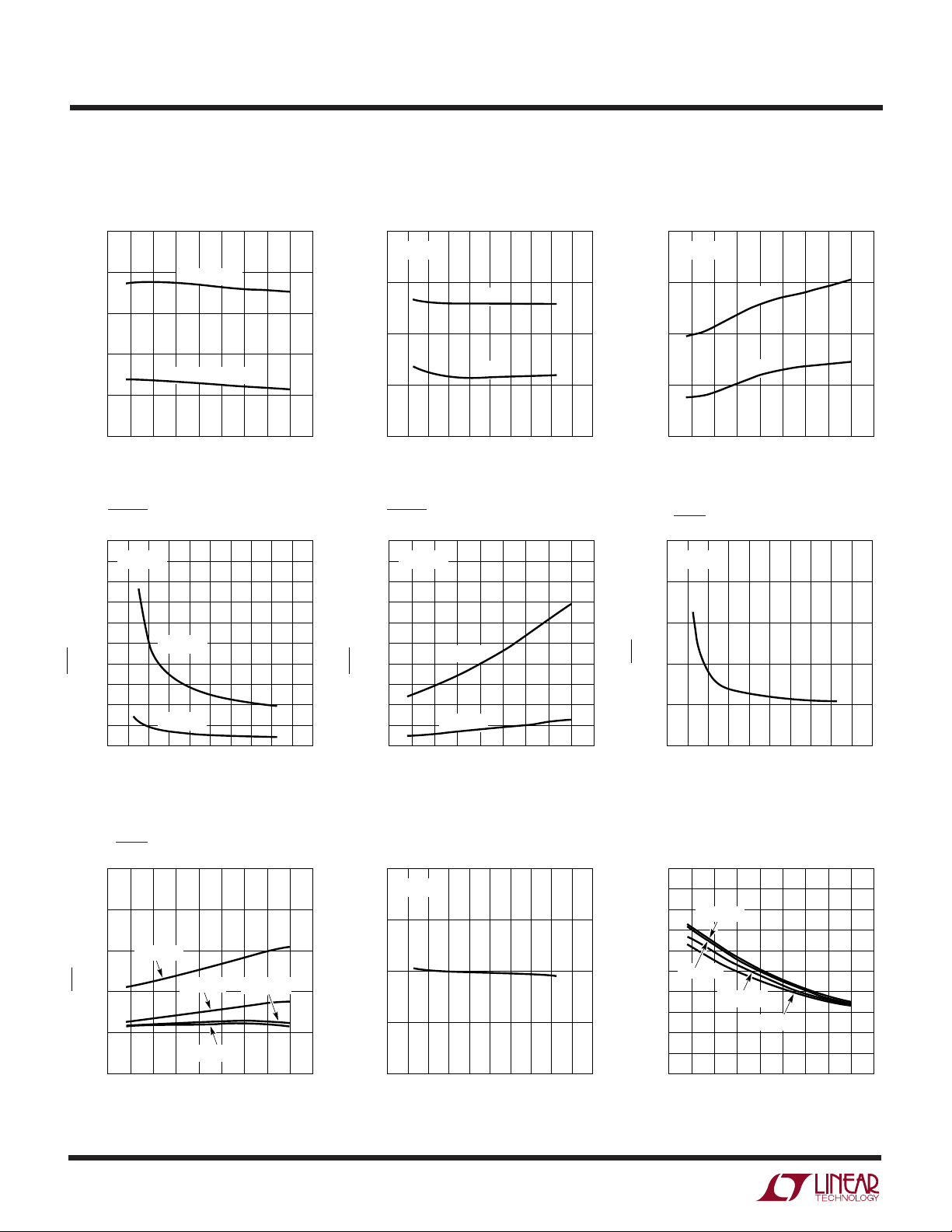
TYPICAL PERFOR A CE CHAR ACTERISTICS
ICC vs V
CC
6
TA = 25°C
= I
+ I
I
CC
CC1
5
VCC = V
4
3
(mA)
CC
I
2
1
0
2
I
vs V
CC2
5
TA = 25°C
4
3
(mA)
CC2
I
2
V
CC1
1
0
02468101214161820
CC2
= V
CC1
6 10 14 184 8 12 16
= ON1 = ON2
CC2
VCC (V)
CC2
V
= 15V
CC1
V
= 12V
CC1
= 3V
V
= 5V
CC1
V
(V)
CC2
1647-1/2/3 G01
1647-1/2/3 G04
ICC vs Temperature I
6
ICC = I
+ I
CC1
VCC = V
5
4
3
(mA)
CC
I
2
1
0
–75 –50 –25 0 25 50 75 100 125 150
(V
GATE
20
18
16
14
) (V)
12
CC
10
– V
8
GATE
(V
6
4
2
0
02468101214161820
CC2
= V
CC1
VCC = 15V VCC = 12V
VCC = 5V
– VCC) vs V
= ON1 = ON2
CC2
TEMPERATURE (°C)
CC
TA = 25°C
= V
V
CC
VCC (V)
CC1
VCC = 3V
1647-1/2/3 G02
= V
CC2
1647-1/2/3 G05
vs V
CC1
5
4
3
(mA)
CC1
I
2
1
0
02468101214161820
V
30
25
20
(V)
15
GATE
V
10
5
0
02468101214161820
TA = 25°C
V
CC1
vs V
GATE
CC2
= 15V
V
CC1
CC
V
= 5V
CC1
V
= 12V
CC1
V
VCC (V)
= 3V
CC2
(V)
TA = 25°C
V
CC
= V
CC1
1647-1/2/3 G03
= V
CC2
1647-1/2/3 G06
(V
– VCC) vs Temperature V
GATE
20
18
16
14
) (V)
12
CC
10
– V
8
GATE
(V
6
4
2
0
–75 –50 –25 0 25 50 75 100 125 150
VCC = 12V
VCC = 5V
VCC = 15V
TEMPERATURE (°C)
VCC = 3V
VCC = V
CC1
4
= V
CC2
1647-1/2/3 G07
vs Temperature (V
GATE
35
VCC = 15V
30
25
VCC = 5V
20
(V)
GATE
15
V
VCC = 3V
10
5
0
–75 –50 –25 0 25 50 75 100 125 150
TEMPERATURE (°C)
VCC = 12V
VCC = V
CC1
= V
CC2
1647-1/2/3 G08
– V
GATE1
20
V
18
CC1
16
14
) (V)
12
CC1
10
– V
8
GATE1
(V
6
V
4
2
0
02468101214161820
) vs Temperature
CC1
= 12V
V
= 5V
CC1
= 3V
CC1
V
CC2
(V)
V
CC1
= 15V
TA = 25°C
(LTC1647-3)
1647-1/2/3 G09
Page 5
LTC1647-1/LTC1647-2/LTC1647-3
UW
TYPICAL PERFOR A CE CHAR ACTERISTICS
V
vs V
GATE1
35
V
30
25
V
20
(V)
GATE1
15
V
10
5
0
02468101214161820
CC1
CC1
= 15V
= 12V
CC2
V
= 5V
CC1
V
= 3V
CC1
TA = 25°C
(LTC1647-3)
V
(V)
CC2
GATE Output Sink Current vs V
100
TA = 25°C
90
80
70
60
50
40
30
20
GATE OUTPUT SINK CURRENT (µA)
10
0
02468101214161820
VCC (V)
1647-1/2/3 G10
CC
1647-1/2/3 G13
GATE Output Source Current vs
V
CC
14
TA = 25°C
13
= V
V
12
11
10
9
8
7
GATE OUTPUT SOURCE CURRENT (µA)
6
02468101214161820
=V
CC
CC1
CC2
VCC (V)
GATE Output Sink Current vs
Temperature
55
VCC = 5V
54
53
52
51
50
49
48
47
GATE OUTPUT SINK CURRENT (µA)
46
45
–75 –50 –25 0 25 50 75 100 125 150
TEMPERATURE (°C)
1647-1/2/3 G11
1647-1/2/3 G14
GATE Output Source Current vs
Temperature
14
VCC = V
13
12
11
10
9
8
7
GATE OUTPUT SOURCE CURRENT (µA)
6
–75 –50 –25 0 25 50 75 100 125 150
= V
= 5V
CC1
CC2
TEMPERATURE (°C)
GATE Fast Pull-Down Current vs
V
CC
60
TA = 25°C
55
50
45
40
35
GATE FAST PULL-DOWN CURRENT (mA)
30
02468101214161820
VCC (V)
1647-1/2/3 G12
1647-1/2/3 G15
GATE Fast Pull-Down Current vs
Temperature
80
VCC = V
70
60
50
40
30
20
10
GATE FAST PULL-DOWN CURRENT (mA)
0
–75 –50 –25 0 25 50 75 100 125 150
= V
CC1
= 5V
CC2
TEMPERATURE (°C)
1647-1/2/3 G16
Circuit Breaker Trip Voltage vs
V
CC
60
TA = 25°C
58
56
54
52
50
48
46
44
42
CIRCUIT BREAKER TRIP VOLTAGE (mV)
40
02468101214161820
VCC (V)
1647-1/2/3 G17
Circuit Breaker Trip Voltage vs
Temperature
60
58
56
54
52
50
48
46
44
42
CIRCUIT BREAKER TRIP VOLTAGE (mV)
40
–75 –50 –25 0 25 50 75 100 125 150
VCC = 15V
= 12V
V
CC
VCC = 5V
= 3V
V
CC
TEMPERATURE (°C)
1647-1/2/3 G18
5
Page 6
LTC1647-1/LTC1647-2/LTC1647-3
UW
TYPICAL PERFOR A CE CHAR ACTERISTICS
Undervoltage Lockout Threshold
vs Temperature ON Threshold Voltage vs V
2.6
2.5
2.4
2.3
2.2
UNDERVOLTAGE LOCKOUT THRESHOLD (V)
2.1
–75 –50 –25 0 25 50 75 100 125 150
FAULT VOL vs V
2.0
TA = 25°C
1.8
1.6
1.4
(V)
1.2
OL
1.0
0.8
FAULT V
0.6
0.4
0.2
0
02468101214161820
RISING EDGE
FALLING EDGE
TEMPERATURE (°C)
CC
IOL = 5mA
IOL = 1mA
VCC (V)
1647-1/2/3 G19
1647-1/2/3 G22
1.35
TA = 25°C
1.30
1.25
1.20
ON THRESHOLD VOLTAGE (V)
1.15
02468101214161820
HIGH
LOW
VCC (V)
FAULT VOL vs Temperature T
2.0
VCC = 5V
1.8
1.6
1.4
(V)
1.2
OL
1.0
0.8
FAULT V
0.6
0.4
0.2
0
–75 –50 –25 0 25 50 75 100 125 150
IOL = 5mA
IOL = 1mA
TEMPERATURE (°C)
CC
1647-1/2/3 G20
1647-1/2/3 G23
ON Threshold Voltage vs
Temperature
1.35
VCC = 5V
1.30
1.25
1.20
ON THRESHOLD VOLTAGE (V)
1.15
–75 –50 –25 0 25 50 75 100 125 150
FAULT
1.0
TA = 25°C
0.8
0.6
(µs)
FAULT
T
0.4
0.2
0
02468101214161820
HIGH
LOW
TEMPERATURE (°C)
vs V
CC
VCC (V)
1647-1/2/3 G21
1647-1/2/3 G24
T
vs Temperature Circuit Breaker Reset Time vs V
FAULT
1.0
0.8
0.6
(µs)
FAULT
T
0.4
0.2
VCC = 3V
VCC = 5V
0
–75 –50 –25 0 25 50 75 100 125 150
TEMPERATURE (°C)
VCC = 12V
VCC = 15V
6
1647-1/2/3 G25
70
TA = 25°C
60
50
40
CIRCUIT BREAKER RESET TIME (µs)
30
02468101214161820
VCC (V)
CC
1647-1/2/3 G26
Circuit Breaker Reset Time vs
Temperature
60
58
56
54
52
50
48
46
44
CIRCUIT BREAKER RESET TIME (µs)
42
40
VCC = 3V
VCC = 5V
VCC = 12V
VCC = 15V
–75 –50 –25 0 25 50 75 100 125 150
TEMPERATURE (°C)
1647-1/2/3 G27
Page 7

UUU
PI FU CTIO S
V
(LTC1647-3): Channel 1 Positive Supply Input. The
CC1
supply range for normal operation is 2.7V to 16.5V. The
supply current, I
voltage lockout (UVLO) circuit disables GATE 1 until the
supply voltage at V
2.47V). GATE 1 is held at ground potential until UVLO
deactivates. If ON1 is high and V
threshold voltage, GATE 1 is pulled high by a 10µA current
source. If V
CC1
immediately to ground. The internal reference and the
common charge pump are powered from the higher of the
two VCC inputs, V
V
(LTC1647-3): Channel 2 Positive Supply Input. See
CC2
V
for functional description.
CC1
VCC: The Common Positive Supply Input for the LTC1647-1
and the LTC1647-2. V
nected together.
GND: Chip Ground.
, is typically 1mA. Channel 1’s under-
CC1
is greater than V
CC1
falls below (V
or V
CC1
CC1
CC2
and V
LKO
.
is above the UVLO
CC1
– V
), GATE 1 is pulled
LKH
are internally con-
CC2
(typically
LKO
LTC1647-1/LTC1647-2/LTC1647-3
FAULT 1: Channel 1 Open-Drain Fault Status Output.
FAULT 1 pin pulls low after 0.3µs (t
breaker measures greater than 50mV across the sense
resistor connected between V
and SENSE 1. If FAULT 1
CC1
pulls low, GATE 1 also pulls low. FAULT 1 remains low until
ON1 is pulled low for at least one t
RESET
FAULT 2: Channel 2 Open-Drain Fault Status Output. See
FAULT 1 for functional description.
SENSE 1: Channel 1 Circuit Breaker Current Sense Input.
Load current is monitored by a sense resistor connected
between V
and SENSE 1. The circuit breaker trips if the
CC1
voltage across the sense resistor exceeds 50mV (VCB). To
disable the circuit breaker, connect SENSE 1 to V
order to obtain optimum performance, use Kelvin-sense
connections between the VCC and SENSE pins to the
current sense resistor.
SENSE 2: Channel 2 Circuit Breaker Current Sense Input.
See SENSE 1 for functional description.
) if the circuit
FAULT
period.
CC1
. In
ON1: Channel 1 ON Input. The threshold at the ON1 pin is
set at 1.28V with 70mV hysteresis. If UVLO and the circuit
breaker of channel 1 are inactive, a logic high at ON1
enables the 10µA charge pump current source, pulling the
GATE 1 pin above V
. If the ON1 pin is pulled low, the
CC1
GATE 1 pin is pulled to ground by a 50µA current sink.
ON1 resets channel 1’s electronic circuit breaker by pull-
ing ON1 low for greater than one t
period (50µs). A
RESET
low-to-high transition at ON1 restarts a normal GATE 1
pull-up sequence.
ON2: Channel 2 ON Input. See ON1 for functional description.
GATE 1: Channel 1 N-Channel MOSFET Gate Drive Output.
An internal charge pump guarantees at least 10V of gate
drive from a 5V supply. Two Zener clamps are incorporated at the GATE 1 pin; one Zener clamps GATE 1
approximately 15V above VCC and the second Zener
clamps GATE 1 appoximately 28V above GND. The rise
time at GATE 1 is set by an external capacitor connected
between GATE 1 and GND and an internal 10µA current
source provided by the charge pump. The fall time at GATE
1 is set by the 50µA current sink if ON1 is pulled low. If the
circuit breaker is tripped or the supply voltage hits the
UVLO threshold, a 50mA current sink rapidly pulls GATE 1
low.
GATE 2: Channel 2 N-Channel MOSFET Gate Drive Output.
See GATE 1 for functional description.
NC: No Connection.
7
Page 8

LTC1647-1/LTC1647-2/LTC1647-3
W
BLOCK DIAGRA S
LTC1647-1
+
50mV
–
+
8SENSE 1
2ON1
1.21V
–
+
–
50µs
FILTER
CHANNEL ONE
CP
10µA
6 GATE 1
2.45V
UVL
1V
CC
4GND
7SENSE 2 5 GATE 2
ON2
3
REFERENCE 1.21V
CHARGE
PUMP
(DUPLICATE OF CHANNEL ONE)
CP
CHANNEL TWO
50µA
LTC1647-2
+
50mV
–
+
8SENSE 1
2ON1/FAULT 1
1.21V
–
+
–
50µs
FILTER
CHANNEL ONE
CP
10µA
1647-1/2/3 BD1
6 GATE 1
8
ON2/FAULT 2
2.45V
UVL
1V
CC
4GND
7SENSE 2 5 GATE 2
3
REFERENCE 1.21V
(DUPLICATE OF CHANNEL ONE)
CHARGE
PUMP
CHANNEL TWO
FAULT
CP
50µA
1647-1/2/3 BD2
Page 9

W
BLOCK DIAGRA S
1V
CC1
15SENSE 1
2ON1
+
–
50mV
1.21V
LTC1647-1/LTC1647-2/LTC1647-3
LTC1647-3
50µs
FILTER
CHANNEL ONE
CP
10µA
13 GATE 1
+
–
+
–
2.45V
UVL
REFERENCE 1.21V
WUU
CHARGE
PUMP
CHANNEL TWO
(DUPLICATE OF CHANNEL ONE)
SENSE 2
3FAULT 1
8GND
16V
CC2
14
4ON2
5FAULT 2
U
APPLICATIO S I FOR ATIO
VCC Selection Circuit
The LTC1647-3 features separate supply inputs (V
V
) for each channel. The reference and charge pump
CC2
circuit draw supply current from the higher of the two
supplies. An internal VCC selection circuit detects and
makes the power connection automatically. This allows a
3V channel to have standard MOSFET gate overdrive when
the other channel is 5V. An internal Zener clamps GATE
about 15V above VCC.
If both supplies are connected together (internally for
LTC1647-1 and LTC1647-2 or externally for LTC1647-3),
the reference and charge pump circuit draw equal current
from both pins.
Electronic Circuit Breaker
Each channel of the LTC1647 features an electronic circuit
breaker to protect against excessive load current and
CC1
and
50µA
FAULT
V
CP
CC
SELECTION
12 GATE 2
1647-1/2/3 BD3
short-circuits. Load current is monitored by sense resistor R1 as shown in Figure 1. The circuit breaker threshold,
VCB, is 50mV and it exhibits a response time, t
FAULT
, of
approximately 300ns. If the voltage between VCC and
SENSE exceeds VCB for more than t
, the circuit
FAULT
breaker trips and immediately pulls GATE low with a 50mA
current sink. The MOSFET turns off and FAULT pulls low.
The circuit breaker is cleared by pulling the ON pin low for
a period of at least t
(50µs). A timing diagram of these
RESET
events is shown in Figure 2.
The value of the sense resistor R1 is given by
R1 = VCB/I
TRIP
(Ω)
where VCB is the circuit breaker trip voltage (50mV) and
I
is the value of the load current at which the circuit
TRIP
breaker trips. Kelvin-sense layout techniques between the
sense resistor and the VCC and SENSE pins are highly
recommended for proper operation.
9
Page 10

LTC1647-1/LTC1647-2/LTC1647-3
U
WUU
APPLICATIO S I FOR ATIO
The circuit breaker trip voltage has a tolerance of 20%;
combined with a 5% sense resistor, the total tolerance is
25%. Therefore, calculate R1 based on a trip current I
of no less than 125% of the maximum operating current.
Do not neglect the effect of ripple current, which adds to
the maximum DC component of the load current. Ripple
current may arise from any of several sources, but the
worst offenders are switching supplies.
A switching regulator on the load side will attempt to draw
some ripple current from the backplane and this current
passes through the sense resistor. Similarly, output ripple
from a switching regulator supplying the backplane will
flow through the sense resistor and into the load capacitor.
Minimize the effects of ripple current by either filtering the
V
line or adding an RC filter to the SENSE pin. A series
OUT
inductance of 1µH to 10µH inserted between Q1 and C
is adequate ripple current suppression in most cases.
Alternatively, a filter, consisting of R3 and C3(Figure 3),
simply filters the ripple component from the SENSE pin at
the expense of response time. The added delay is given by
t
= –R3•C3•ln[1 – (VCB/R1 – IAV)/(IPK – IAV)]
DELAY
V
FAULT
R1
CC
R3
10k
ON
0.01Ω
1
SENSE
V
CC
2
ON1
FAULT
GND
LTC1647-3
3
8
Figure 1. Supply Control Circuitry
V
ON
V
V
–
CC
SENSE
V
GATE
V
FAULT
Q1
IRF7413
15 13
GATE
t
FAULT
t
RESET
R2
10Ω
+
C1
10nF
1647-1/2/3 F01
1647-1/2/3 F02
C
V
LOAD
TRIP
LOAD
OUT
R3
1.5k
Q1
IRF7413
GATE
R2
10Ω
V
OUT
+
C
LOAD
IPK = 7.5A
= 2.5A
I
AV
= VCB/R1 = 5A
I
TRIP
= 10µs
t
DELAY
C1
10nF
1647-1/2/3 F03
R1
V
CC
0.01Ω
C3
10nF
SENSE
V
CC
LTC1647
Figure 3. Filtering Current Ripple/Glitches
Power MOSFET Selection
Power MOSFETs are classified into two catagories: standard MOSFETs (R
level MOSFETs (R
specified at VGS = 10V) and logic-
DS(ON)
specified at VGS = 5V). The
DS(ON)
absolute maximum rating for VGS is typically 20V for
standard MOSFETs. The maximum rating for logic-level
MOSFETs is lower and ranges from 8V to 16V depending
on the manufacturer and specific part number. Some
logic-level MOSFETs have a 20V maximum VGS rating. The
LTC1647 is primarily targeted for standard MOSFETs; low
supply voltage applications should use logic-level
MOSFETs. GATE overdrive as a function of VCC is illustrated in the Typical Performance Curves. If lower GATE
overdrive is desired, connect a diode in series with a Zener
between GATE and VCC or between GATE and V
OUT
as
shown in Figure 4.
The R
of the external pass transistor must be low to
DS(ON)
make VDS a small percentage of VCC. At VCC = 3.3V, VDS +
VCB = 0.1V yields 3% error at maximum load current. This
restricts the choice of MOSFETs to very low R
higher VCC voltages, the R
requirement can be
DS(ON)
DS(ON)
. At
relaxed. MOSFET package dissipation (PD and TJ) may
restrict the value of R
V
CC
R1
D1*D21N4148 D4*
*USER SELECTED VOLTAGE CLAMP
1N4688 (5V)
1N4692 (7V): LOGIC-LEVEL MOSFET
1N4695 (9V)
1N4702 (15V): STANDARD-LEVEL MOSFET
DS(ON)
.
Q1
D2
1N4148
V
OUT
1647-1/2/3 F04
10
Figure 2. Current Fault Timing
Figure 4. Optional Gate Clamp
Page 11

LTC1647-1/LTC1647-2/LTC1647-3
U
WUU
APPLICATIO S I FOR ATIO
Power Supply Ramping
V
is controlled by placing MOSFET Q1 in the power
OUT
path (Figure 1). R1 provides load current fault detection
and R2 prevents MOSFET high frequency oscillation. By
ramping the gate of the pass transistor at a controlled rate
(dV/dt = 10µA/C1), the transient surge current
(I = C
backplane is limited to a safe value when the board is
inserted into the connector.
When power is first applied to VCC, the GATE pin pulls low.
A low-to-high transition at the ON pin initiates GATE rampup. The rising dV/dt of GATE is set by 10µA/C1 (Figure 5),
where C1 is the total external capacitance between GATE
and GND. The ramp-up time for V
t = (VCC•C1)/10µA.
V
CC
V
+ ∆
CC
•dV/dt = 10µA•C
LOAD
V
+ ∆
GATE
V
CC
0V
V
CC
0V
V
GATE
V
CC
0V
V
CC
0V
/C1) drawn from the main
LOAD
is equal to
OUT
V
GATE
RAMP-UP
SLOPE = 10µA/C1
RAMP-DOWN
SLOPE = –50µA/C1
V
OUT
C
DISCHARGES
LOAD
V
ON
Figure 5. Supply Turn-On/Off with ON
V
OUT OF UVLO
V
LKO
RAMP-UP
SLOPE = 10µA/C1
C
DISCHARGES
LOAD
V
UNPLUGGED
GATE
V
OUT
CC
V
CC
V
DROOP
GATE
DUE TO V
FAST RAMP-DOWN
AT UNDERVOLTAGE
LOCKOUT
INTO UVLO
V
LKO
1647-1/2/3 F05
CC
V
–
LKH
1647-1/2/3 F06
A high-to-low transition at the ON pin initiates a GATE
ramp-down at a slope of –50µA/C1. This rate is usually
adequate as the supply bypass capacitors take time to
discharge through the load.
If the ON pin is connected to VCC, or is pulled high before
VCC is first applied, GATE is held low until VCC rises above
the undervoltage lockout threshold, V
(Figure 6). Once
LKO
the threshold is exceeded, GATE ramps at a controlled rate
of 10µA/C1. When the power supply is disconnected, the
body diode of Q1 holds VCC about 700mV below V
GATE voltage droops at a rate determined by VCC. If V
drops below V
LKO
– V
, the LTC1647 enters UVLO and
LKH
OUT
. The
CC
GATE pulls down to GND.
Autoretry
The LTC1647-2 and LTC1647-3 are designed to allow an
automatic reset of the electronic circuit breaker after a
fault condition occurs. This is accomplished by pulling the
ON/FAULT (LTC1647-2) pin or the ON and FAULT pins tied
together (LTC1647-3) high through a resistor, R3, as
shown in Figure 7. An autoretry sequence begins if a fault
occurs. If the circuit breaker trips, FAULT pulls the ON pin
low. After a t
V
CC
ON
(5V LOGIC)
FAULT
C3
0.1µF
VCC – V
interval elapses, FAULT resets and R3
RESET
Q1
IRF7413
R2
10Ω
86
GATE
LTC1647-2
t
RESET
t
DELAY
t
RAMP
SENSE
V
V
FAULT
GATE
R3
15k
2
ON/FAULT
4
GND
R1
0.01Ω
1
SENSE
V
CC
+
1647-1/2/3 F07
C
LOAD
C1
10nF
V
OUT
Figure 7. Autoretry Sequence
11
Page 12

LTC1647-1/LTC1647-2/LTC1647-3
U
WUU
APPLICATIO S I FOR ATIO
pulls the ON pin up. C3 delays GATE turn-on until the
voltage at the ON pin exceeds VIH. The delay time is
t
= –R3•C3•ln[1–(VIH – VOL)/(VON – VOL)]
DELAY
GATE ramps up at 10µA/C1 until Q1 conducts. If V
still shorted to GND, the cycle repeats. The ramp interval
is about t
voltage of the external MOSFET.
Hot Circuit Insertion
When circuit boards are inserted into a live backplane or
a device bay, the supply bypass capacitors on the board
can draw huge transient currents from the backplane or
the device bay power bus as they charge up. The transient
currents can damage the connector pins and glitch the
system supply, causing other boards in the system to
reset or malfunction.
The LTC1647 is designed to turn two positive supplies on
and off in a controlled manner, allowing boards to be safely
inserted or removed from a live backplane or device bay.
The LTC1647 can be located before or after the connector
as shown in Figure 8. A staggered PCB connector can
sequence pin conections when plugging and unplugging
circuit boards. Alternatively, the control signal can be
generated by processor control.
Ringing
= VTH•C1/10µA where VTH is the threshold
RAMP
OUT
is
No bulk capacitance is present to slow the rate of rise and
heavily damp the parasitic resonance. Instead, the fast
edge shock excites a resonant circuit formed by a combination of wiring harness, backplane and circuit board
parasitic inductances and MOSFET capacitance. In theory,
the peak voltage should rise to 2X the input supply, but in
practice the peak can reach 2.5X, owing to the effects of
voltage dependent MOSFET capacitance.
The absolute maximum VCC potential for the LTC1647 is
17V; any circuit with an input of more than 6.8V should be
scrutinized for ringing. A well-bypassed backplane should
not escape suspicion: circuit board trace inductances of as
little as 10nH can produce sufficient ringing to overvoltage
VCC.
Check ringing with a fast storage oscilloscope (such as a
LECROY 9314AL DSO) by attaching coax or a probe to V
and GND, then repeatedly inserting the circuit board into
the backplane. Figures 9a and 9b show typical results in a
12V application with different VCC lead lengths. The peak
amplitude reaches 22V, breaking down the ESD protection
diode in the process.
There are two methods for eliminating ringing: clipping
and snubbing. A transient voltage suppressor is an effective means of limiting peak voltage to a safe level.
Figure 10 shows the effect of adding an ON Semiconductor, 1SMA12CAT3, on the waveform of Figure 9.
CC
Good engineering practice calls for bypassing the supply
rail of any circuit. Bypass capacitors are often placed at the
supply connection of every active device, in addition to one
or more large value bulk bypass capacitors per supply rail.
If power is connected abruptly, the bypass capacitors slow
the rate of rise of voltage and heavily damp any parasitic
resonance of lead or trace inductance working against the
supply bypass capacitors.
The opposite is true for LTC1647 Hot Swap circuits on a
daughterboard. In most cases, on the powered side of the
MOSFET switch (VCC) there is no supply bypass capacitor
present. An abrupt connection, produced by plugging a
board into a backplane connector, results in a fast rising
edge applied to the VCC line of the LTC1647.
12
Figures 11a and 11b show the effects of snubbing with
different RC networks. The capacitor value is chosen as
10X to 100X the MOSFET C
selected for best damping—1Ω to 50Ω depending on the
value of parasitic inductance.
Supply Glitching
LTC1647 Hot Swap circuits on the backplane are generally
used to provide power-up/down sequence at insertion/
removal as well as overload/short-circuit protection. If a
short-circuit occurs at supply ramp-up, the circuit breaker
trips. The partially enhanced MOSFET, Q1, is easily disconnected without any supply glitch.
under bias and R is
OSS
Page 13

LTC1647-1/LTC1647-2/LTC1647-3
U
WUU
APPLICATIO S I FOR ATIO
If a dead short occurs after a supply connection is made
(Figure 12), the sense resistor R1 and the R
enhanced Q1 provide a low impedance path for nearly
unlimited current flow. The LTC1647 discharges the GATE
pin in a few microseconds, but during this discharge time
current on the order of 150 amperes flows from the V
power supply. This current spike glitches the power supply, causing VCC to dip (Figure 12a and 12b).
On recovery from overload, some supplies may overshoot. Other devices attached to this supply may reset or
malfunction and the overshoot may also damage some
components. An inductor (1µH to 10µH) in series with
Q1’s source limits the short-circuit di/dt, thereby limiting
the peak current and the supply glitch (Figure 12c and
12d). Additional power supply bypass capacitance also
reduces the magnitude of the VCC glitch.
DS(ON)
of fully
CC
VID Power Controller
The two Hot Swap channels of the LTC1647 are ideally
suited for VID power control in portable computers.
Figure 13 shows an application using the LTC1647-2 on
the system side of the device bay interface (1394 PHY and/
or USB). The controller detects the presence of a peripheral in each device bay and controls the LTC1647-2. The
timing waveform illustrates the following sequence of
events: t1, rising out of undervoltage lockout with GATE 1
ramping up; t2, load current fault at R1; t3, circuit breaker
resets with R5/C3 delay; t4/t5, controller gates off/on
device supply with RC delay; t6, device enters undervoltage lockout.
If C6 is not connected in Figure 13, FAULT 2 and ON2 will
have similar waveforms. t7 initiates an ON sequence; t8, a
load fault is detected at R7 with FAULT 2 pulling low. If the
controller wants to stretch the interval between retries, it
can pull ON2 low at t9 ( t9 – t8 < 0.4•t
controller initiates a new power-up/down sequence.
). At t10/t11, the
RESET
13
Page 14

LTC1647-1/LTC1647-2/LTC1647-3
U
WUU
APPLICATIO S I FOR ATIO
V
CC
R5R4
ON
Q2
V
CC
2
ON
3
FAULT
8
GND
STAGGERED PCB
EDGE CONNECTOR
FAULT
V
FAULT
R3
CC
BACKPLANE
CONNECTOR
R4
BACKPLANE
R1
1
SENSE
LTC1647-3
(a) HOT SWAP CONTROLLER ON MOTHERBOARD
Q1
R2
15 13
GATE
CONNECTOR
C1
R1
STAGGERED PCB
EDGE CONNECTOR
Q1
+
R2
C
+
V
LOAD
OUT
C
V
LOAD
OUT
1
V
2
3
8
CC
ON
FAULT
GND
R3
(b) HOT SWAP CONTROLLER ON DAUGHTERBOARD
15 13
SENSE
LTC1647-3
Figure 8. Staggered Pins Connection
C1
GATE
1647-1/2/3 F08
14
Page 15

LTC1647-1/LTC1647-2/LTC1647-3
U
WUU
APPLICATIO S I FOR ATIO
8'
POWER
LEADS
+
12V
–
24V
SCOPE
PROBE
R1
0.01Ω
LTC1647
Q1
IRF7413
24V
R2
10Ω
+
1647-1/2/3 F09
C
LOAD
C1
10nF
V
OUT
4V/DIV
0V
1µs/DIV
(a) Undamped V
CC
Waveform (48" Leads)
1647-1/2/3 F09a
Figure 9. Ring Experiment
4V/DIV
0V
1µs/DIV
(b) Undamped V
CC
Waveform (8" Leads)
1647-1/2/3 F09b
15
Page 16

LTC1647-1/LTC1647-2/LTC1647-3
1µs/DIV
1647-1/2/3 F10a
2V/DIV
0V
12V
U
WUU
APPLICATIO S I FOR ATIO
R1
0.01Ω
POWER
LEADS
+
12V
–
ON SEMICONDUCTOR
* 1SMA12CAT3
BACKPLANE CONNECTOR
D1*
PCB EDGE CONNECTOR
LTC1647
Figure 10. Transient Suppressor Clamp
Q1
IRF7413
R2
10Ω
+
V
OUT
C
LOAD
C1
10nF
1647-1/2/3 F10
VCC Waveform Clamped
by a Transient Suppressor
12V
2V/DIV
0V
12V
+
–
1µs/DIV
POWER
LEADS
PCB EDGE CONNECTOR
BACKPLANE CONNECTOR
1647-1/2/3 F11a
R3
10Ω
C1
0.1µF
R1
0.01Ω
LTC1647
2V/DIV
12V
0V
Q1
IRF7413
R2
10Ω
+
V
OUT
C
LOAD
C1
10nF
1647-1/2/3 F11
1µs/DIV
1647-1/2/3 F11b
16
(a) VCC Waveform Damped
by a Snubber (15Ω, 6.8nF)
(b) VCC Waveform Damped
by a Snubber (10Ω, 0.1µF)
Figure 11. Snubber “Fixes”
Page 17

LTC1647-1/LTC1647-2/LTC1647-3
1µs/DIV
4V/DIV
1647-1/2/3 F12b
V
CC
GATE
1µs/DIV
4V/DIV
1647-1/2/3 F12d
GATE
V
CC
U
WUU
APPLICATIO S I FOR ATIO
SUPPLY
GLITCH
+
+
12V
–
C2
100µF
R1
0.01Ω
LTC1647
Q1
IRF7413L12µH
R2
10Ω
C1
10nF
1647-1/2/3 F12
SHORT-CIRCUIT FAULT
BOARD WITH POSSIBLE
BACKPLANE CONNECTOR
25A/DIV
1µs/DIV
(a) VCC Short-Circuit
Supply Current Glitch
without Any Limiting
5A/DIV
1µs/DIV
(c) VCC Short-Circuit
Supply Current Glitch with
2µH Series Inductor
1647-1/2/3 F12a
(b) VCC Supply Glitch
without Any Limiting
1647-1/2/3 F12c
(d) VCC Supply Glitch
with 2µH Series Inductor
Figure 12. Supply Glitch
17
Page 18

LTC1647-1/LTC1647-2/LTC1647-3
U
WUU
APPLICATIO S I FOR ATIO
R1
3.3V V
SUPPLY
ID
FAULT 1
DEVICE BAY
CONTROLLER
WITH 1394 PHY
AND/OR USB
FAULT 2
0.1Ω
ON1
R5
10Ω
C3
0.1µF
ON2
R6
10Ω
C6
0.1µF
R7
0.1Ω
1
V
CC
2
ON1/FAULT 1
3
ON2/FAULT 2
4
GND
Q1
1/2 MMDF3N02HD
86
SENSE 1
SENSE 2
GATE 1
LTC1647-2
GATE 2
75
Q2
1/2 MMDF3N02HD
R2
10Ω
R8
10Ω
DEVICE #1
R3** R4**C
C1
10nF
*C
** R3, R4, R7 AND R8 ARE OPTIONAL DISCHARGE
C4
10nF
R9** R10**C
+
CONNECTOR #1
IS USER-SELECTED BASED
LOAD
ON THE DEVICE REQUIREMENTS
RESISTORS WHEN DEVICES ARE POWERED-OFF
Q1, Q2: ON SEMICONDUCTOR
+
CONNECTOR #2
LOAD
DEVICE #2
LOAD
*
*
1394 PHY
AND/OR
USB PORT
1394 PHY
AND/OR
USB PORT
V
FAULT1
V
GATE1
V
FAULT2
V
GATE2
V
ID
V
ON1
V
R1
V
ON2
V
R7
V
LKO
t4 t5
FAULT 1 WAVEFORM SHOWN WITH C3
V
IH
V
IL
t2
t1
FAULT 2 WAVEFORM SHOWN WITHOUT C6
t7
t3 t6
t9 t10 t11
t8
V
V
–
LKO
LKH
V
IH
1647-1/2/3 F13
Figure 13. VID Power Controller with Fault Status and Retry Sequence
18
Page 19

PACKAGE DESCRIPTIO
LTC1647-1/LTC1647-2/LTC1647-3
U
Dimensions in inches (millimeters) unless otherwise noted.
GN Package
16-Lead Plastic SSOP (Narrow 0.150)
(LTC DWG # 05-08-1641)
16
15
0.189 – 0.196*
(4.801 – 4.978)
14
12 11 10
13
0.009
(0.229)
9
REF
0.015
± 0.004
(0.38 ± 0.10)
0.007 – 0.0098
(0.178 – 0.249)
0.016 – 0.050
(0.406 – 1.270)
* DIMENSION DOES NOT INCLUDE MOLD FLASH. MOLD FLASH
SHALL NOT EXCEED 0.006" (0.152mm) PER SIDE
** DIMENSION DOES NOT INCLUDE INTERLEAD FLASH. INTERLEAD
FLASH SHALL NOT EXCEED 0.010" (0.254mm) PER SIDE
0° – 8° TYP
× 45°
S8 Package
8-Lead Plastic Small Outline (Narrow 0.150)
(LTC DWG # 05-08-1610)
0.229 – 0.244
(5.817 – 6.198)
0.053 – 0.068
(1.351 – 1.727)
0.008 – 0.012
(0.203 – 0.305)
8
12
0.189 – 0.197*
(4.801 – 5.004)
7
6
0.150 – 0.157**
(3.810 – 3.988)
5
4
3
678
0.004 – 0.0098
(0.102 – 0.249)
0.0250
(0.635)
BSC
GN16 (SSOP) 1098
5
0.228 – 0.244
(5.791 – 6.197)
0.010 – 0.020
(0.254 – 0.508)
0.008 – 0.010
(0.203 – 0.254)
*
DIMENSION DOES NOT INCLUDE MOLD FLASH. MOLD FLASH
SHALL NOT EXCEED 0.006" (0.152mm) PER SIDE
**
DIMENSION DOES NOT INCLUDE INTERLEAD FLASH. INTERLEAD
FLASH SHALL NOT EXCEED 0.010" (0.254mm) PER SIDE
Information furnished by Linear Technology Corporation is believed to be accurate and reliable.
However, no responsibility is assumed for its use. Linear Technology Corporation makes no representation that the interconnection of its circuits as described herein will not infringe on existing patent rights.
× 45°
0°– 8° TYP
0.016 – 0.050
(0.406 – 1.270)
0.053 – 0.069
(1.346 – 1.752)
0.014 – 0.019
(0.355 – 0.483)
TYP
0.150 – 0.157**
(3.810 – 3.988)
1
3
2
4
0.004 – 0.010
(0.101 – 0.254)
0.050
(1.270)
BSC
SO8 1298
19
Page 20

LTC1647-1/LTC1647-2/LTC1647-3
U
TYPICAL APPLICATIO
Hot Swapping Two Supplies
Two separate supplies can be independently controlled by
using the LTC1647-3. In some applications, sequencing
between the two power supplies is a requirement. For
example, it may be necessary to ramp-up one supply first
before allowing the second supply to power-up, as well as
requiring that this same supply ramp-down last on powerdown. Figure 14’s circuit illustrates how to program the
delays between the two pass transistors using the ON1
Q1
IRF7413
R3
100Ω
15 13
GATE 1
14 1216
R2
10Ω
+
5V SUPPLY
ON1
ON2
FAULT
GND
R5
10kR610k
CONNECTOR
12k
R1
0.01Ω
R4
4.7k
R7
2
3
4
5
8
1
V
CC1
ON1
FAULT 1
ON2
FAULT 2
GND
CC2
SENSE 1
LTC1647-3
SENSE 2 GATE 2V
and ON2 pins (time events t1 to t4). t5 and t7 show both
channels being switched on simultaneously where sequencing is not crucial.
Some applications require that both channels be gated off
if a fault occurs in one channel. This is accomplished in
Figure 14 by using a crisscross FAULT-to-SENSE arrangement of R3/R4 and R7/R8. t6 and t9 illustrate the circuit’s
operation.
V
OUT1
(5A)
C
LOAD
V
C1
10nF
R1
V
R10
V
ON1
V
ON2
t1 t4 t5 t7 t8
V
OUT1
t3t2
t6
t9
12V SUPPLY
R10
0.02Ω
R8
100Ω
Q2
IRF7413
R9
10Ω
C3
10nF
+
C
LOAD
V
OUT2
(2.5A)
V
OUT2
1647-1/2/3 F14
Figure 14. Hot Swapping Two Supplies
RELATED PARTS
PART NUMBER DESCRIPTION COMMENTS
LTC1421 2-Channel Hot Swap Controller 24-Pin, Operates from 3V to 12V and Supports –12V
LTC1422 Hot Swap Controller in SO-8 System Reset Output with Programmable Delay
LT1640L/LT1640H Negative Voltage Hot Swap Controller in SO-8 Operates from –10V to –80V
LT1641 High Voltage Hot Swap Controller in SO-8 Operates from 9V to 80V
LT1642 Fault Protected Hot Swap Controller Operates Up to 16.5V, Protected to 33V
LTC1643L/LTC1643H PCI-Bus Hot Swap Controller 3.3V, 5V and ±12V in Narrow 16-Pin SSOP
LT1645 2-Channel Hot Swap Controller Operates from 1.2V to 12V, Power Sequencing
1647f LT/TP 0100 4K • PRINTED IN USA
LINEAR TECHNOLOGY CORPORATION 1999
20
Linear Technology Corporation
1630 McCarthy Blvd., Milpitas, CA 95035-7417
(408) 432-1900 ● FAX: (408) 434-0507
●
www.linear-tech.com
 Loading...