

Page 1
FEATURES
LTC1594/LTC1598
4- and 8-Channel,
Micropower Sampling
12-Bit Serial I/O A/D Converters
U
DESCRIPTION
■
12-Bit Resolution
■
Auto Shutdown to 1nA
■
Low Supply Current: 320µA Typ
■
Guaranteed ±3/4LSB Max DNL
■
Single Supply 5V Operation
(3V Versions Available: LTC1594L/LTC1598L)
■
Multiplexer: 4-Channel MUX (LTC1594)
8-Channel MUX (LTC1598)
■
Separate MUX Output and ADC Input Pins
■
MUX and ADC May Be Controlled Separately
■
Sampling Rate: 16.8ksps
■
I/O Compatible with QSPI, SPI and MICROWIRETM, etc.
■
Small Package: 16-Pin Narrow SO (LTC1594)
24-Pin SSOP (LTC1598)
U
APPLICATIONS
■
Pen Screen Digitizing
■
Battery-Operated Systems
■
Remote Data Acquisition
■
Isolated Data Acquisition
■
Battery Monitoring
■
Temperature Measurement
The LTC®1594/LTC1598 are micropower, 12-bit sampling
A/D converters that feature 4- and 8-channel multiplexers,
respectively. They typically draw only 320µA of supply
current when converting and automatically power down to
a typical supply current of 1nA between conversions. The
LTC1594 is available in a 16-pin SO package and the
LTC1598 is packaged in a 24-pin SSOP. Both operate on
a 5V supply. The 12-bit, switched-capacitor, successive
approximation ADCs include a sample-and-hold.
On-chip serial ports allow efficient data transfer to a wide
range of microprocessors and microcontrollers over three
or four wires. This, coupled with micropower consumption, makes remote location possible and facilitates transmitting data through isolation barriers.
The circuit can be used in ratiometric applications or with
an external reference. The high impedance analog inputs
and the ability to operate with reduced spans (to 1.5V full
scale) allow direct connection to sensors and transducers
in many applications, eliminating the need for gain stages.
, LTC and LT are registered trademarks of Linear Technology Corporation.
MICROWIRE is a trademark of National Semiconductor Corporation.
U
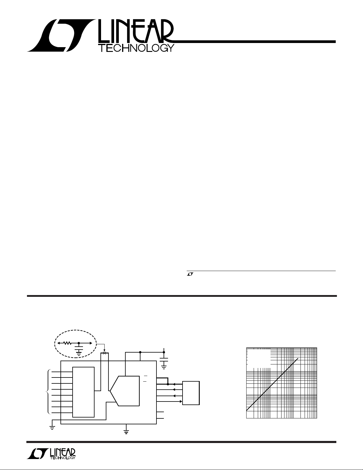
TYPICAL APPLICATION
24µW, 4-Channel, 12-Bit ADC Samples at 200Hz and Runs Off a 5V Supply
OPTIONAL
ADC FILTER
ANALOG
INPUTS
0V TO 5V
RANGE
20
21
22
23
24
1
2
3
8 COM
CH0
CH1
CH2
CH3
CH4
CH5
CH6
CH7
1k
1µF
8-CHANNEL
MUX
18 17 16 15, 19
ADCINMUXOUT
+
V
REFVCC
12-BIT
SAMPLING
ADC
CSADC
CSMUX
–
GND
4, 9
CLK
D
IN
D
OUT
NC
NC
1594/98 TA01
10
6
5, 14
7
11
12
13
5V
1µF
SERIAL DATA LINK
MICROWIRE AND
SPI COMPATABLE
MPU
Supply Current vs Sample Rate
1000
TA = 25°C
= 5V
V
CC
= 5V
V
REF
= 320kHz
f
CLK
100
10
SUPPLY CURRENT (µA)
1
0.1
1 10 100
SAMPLE FREQUENCY (kHz)
1594/98 TA02
1
Page 2
LTC1594/LTC1598
WW
W
U
ABSOLUTE MAXIMUM RATINGS
(Notes 1, 2)
Supply Voltage (VCC) to GND................................... 12V
Voltage
Analog Reference .................... –0.3V to (VCC + 0.3V)
Analog Inputs .......................... –0.3V to (VCC + 0.3V)
Digital Inputs .........................................– 0.3V to 12V
Digital Output .......................... –0.3V to (VCC + 0.3V)
U
W
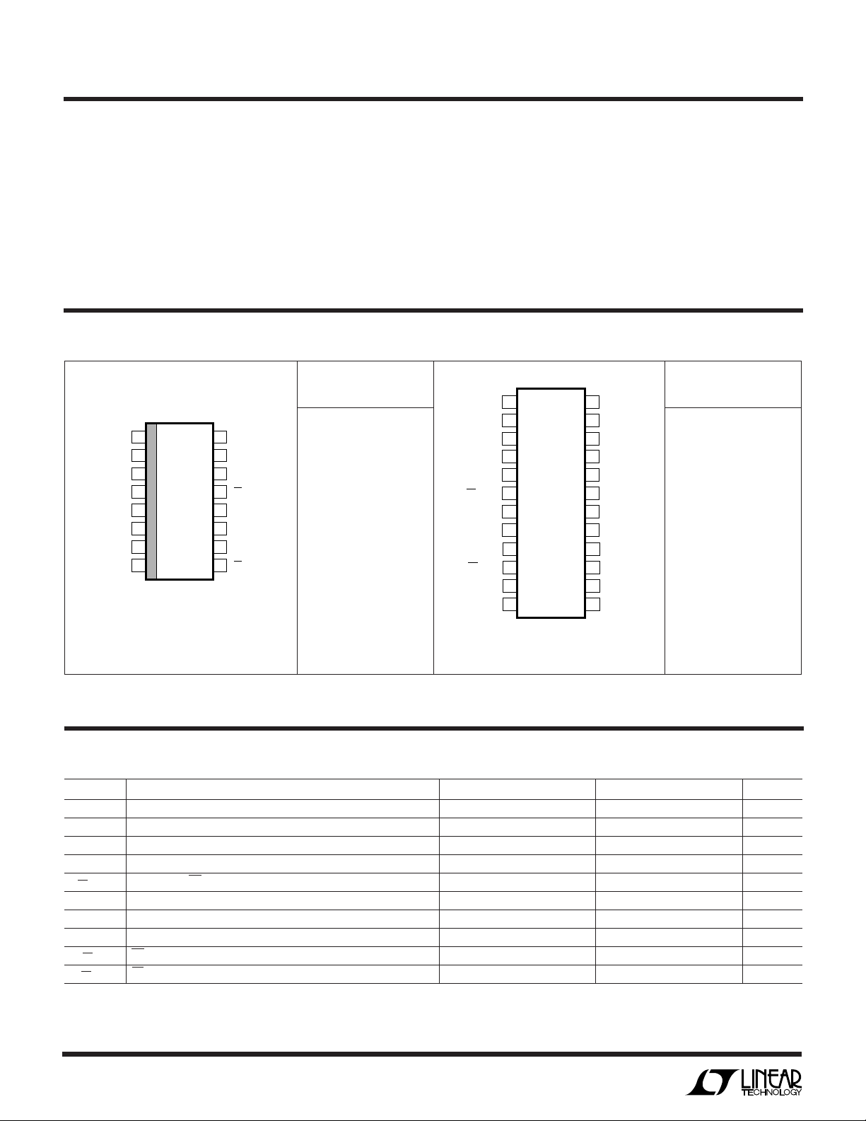
PACKAGE/ORDER INFORMATION
ORDER PART
NUMBER
TOP VIEW
1
CH0
2
CH1
3
CH2
4
CH3
5
ADCIN
6
V
REF
7
COM
8
GND
16-LEAD PLASTIC SO
T
JMAX
16
15
14
13
12
11
10
9
S PACKAGE
= 125°C, θJA = 120°C/ W
V
CC
MUXOUT
D
IN
CSMUX
CLK
V
CC
D
OUT
CSADC
LTC1594CS
LTC1594IS
Power Dissipation.............................................. 500mW
Operating Temperature Range
LTC1594CS/LTC1598CG ......................... 0°C to 70°C
LTC1594IS/LTC1598IG ..................... –40°C to 85°C
Storage Temperature Range ................. –65°C to 150°C
Lead Temperature (Soldering, 10 sec).................. 300°C
U
ORDER PART
NUMBER
LTC1598CG
LTC1598IG
1
CH5
2
CH6
3
CH7
4
GND
5
CLK
6
CSMUX
7
D
IN
8
COM
9
GND
10
CSADC
11
D
OUT
12
NC
24-LEAD PLASTIC SSOP
T
JMAX
TOP VIEW
24
23
22
21
20
19
18
17
16
15
14
13
G PACKAGE
= 150°C, θJA = 110°C/ W
CH4
CH3
CH2
CH1
CH0
V
CC
MUXOUT
ADCIN
V
REF
V
CC
CLK
NC
Consult factory for Military grade parts.
WW
RECOM ENDED OPERATING CONDITIONS
UU
UU
(Note 5)
SYMBOL PARAMETER CONDITIONS MIN TYP MAX UNITS
V
CC
f
CLK
t
CYC
t
hDI
t
suCS
t
suDI
t
WHCLK
t
WLCLK
t
WHCS
t
WLCS
Supply Voltage (Note 3) 4.5 5.5 V
Clock Frequency VCC = 5V (Note 4) 320 kHz
Total Cycle Time f
= 320kHz 60 µs
CLK
Hold Time, DIN After CLK↑ VCC = 5V 150 ns
Setup Time CS↓ Before First CLK↑ (See Operating Sequence) VCC = 5V 1 µs
Setup Time, DIN Stable Before CLK↑ VCC = 5V 400 ns
CLK High Time VCC = 5V 1 µs
CLK Low Time VCC = 5V 1 µs
CS High Time Between Data Transfer Cycles f
CS Low Time During Data Transfer f
= 320kHz 16 µs
CLK
= 320kHz 44 µs
CLK
2
Page 3
LTC1594/LTC1598
UW
CONVERTER AND MULTIPLEXER CHARACTERISTICS
PARAMETER CONDITIONS MIN TYP MAX MIN TYP MAX UNITS
Resolution (No Missing Codes) ● 12 12 Bits
Integral Linearity Error (Note 6) ● ±3 ±3LSB
Differential Linearity Error ● ±3/4 ±1LSB
Offset Error ● ±3 ±3LSB
Gain Error ● ±8 ±8LSB
REF Input Range (Notes 7, 8) 1.5V to V
Analog Input Range (Notes 7, 8) –0.05V to VCC + 0.05V V
MUX Channel Input Leakage Current Off Channel ● ±200 ±200 nA
MUXOUT Leakage Current Off Channel ● ±200 ±200 nA
ADCIN Input Leakage Current (Note 9) ● ±1 ±1 µA
U
(Note 5)
LTC1594CS/LTC1598CG LTC1594IS/LTC1598IG
+ 0.05V V
CC
UW
DYNAMIC ACCURACY
SYMBOL PARAMETER CONDITIONS MIN TYP MAX UNITS
S/(N + D) Signal-to-Noise Plus Distortion Ratio 1kHz Input Signal 71 dB
THD Total Harmonic Distortion (Up to 5th Harmonic) 1kHz Input Signal – 78 dB
SFDR Spurious-Free Dynamic Range 1kHz Input Signal 80 dB
Peak Harmonic or Spurious Noise 1kHz Input Signal – 80 dB
(Note 5) f
SMPL
= 16.8kHz
U
DIGITAL AND DC ELECTRICAL CHARACTERISTICS
SYMBOL PARAMETER CONDITIONS MIN TYP MAX UNITS
V
IH
V
IL
I
IH
I
IL
V
OH
V
OL
I
OZ
I
SOURCE
I
SINK
R
REF
I
REF
I
CC
High Level Input Voltage VCC = 5.25V ● 2.6 V
Low Level Input Voltage VCC = 4.75V ● 0.8 V
High Level Input Current VIN = V
Low Level Input Current VIN = 0V ● –2.5 µA
High Level Output Voltage VCC = 4.75V, IO = 10µA ● 4.0 4.64 V
Low Level Output Voltage VCC = 4.75V, IO = 1.6mA ● 0.4 V
Hi-Z Output Leakage CS = High ● ±3 µA
Output Source Current V
Output Sink Current V
Reference Input Resistance CS = V
Reference Current CS = V
Supply Current CS = VCC, CLK = VCC, DIN = V
CC
VCC = 4.75V, IO = 360µA ● 2.4 4.62 V
= 0V –25 mA
OUT
= V
OUT
CC
IH
CS = V
IL
CC
≥ 760µs, f
t
CYC
t
≥ 60µs, f
CYC
≥ 760µs, f
t
CYC
t
≥ 60µs, f
CYC
≤ 25kHz 90 µA
CLK
≤ 320kHz ● 90 140 µA
CLK
≤ 25kHz 320 µA
CLK
≤ 320kHz ● 320 690 µA
CLK
CC
(Note 5)
● 2.5 µA
45 mA
5000 MΩ
55 kΩ
● 0.001 2.5 µA
● 0.001 ±5 µA
3
Page 4
LTC1594/LTC1598
TEMPERATURE (°C)
–55
92.0
REFERENCE CURRENT (µA)
92.5
93.5
94.0
94.5
–15
25
45 125
1594/98 G03
93.0
–35 5
65
85
105
95.0
VCC = V
REF
= 5V
f
SMPL
= 16.8kHz
f
CLK
= 320kHz
AC CHARACTERISTICS
(Note 5)
SYMBOL PARAMETER CONDITIONS MIN TYP MAX UNITS
t
SMPL
f
SMPL(MAX)
t
CONV
t
dDO
t
dis
t
en
t
hDO
t
f
t
r
t
ON
t
OFF
t
OPEN
C
IN
Analog Input Sample Time See Figure 1 in Applications Information 1.5 CLK Cycles
Maximum Sampling Frequency See Figure 1 in Applications Information ● 16.8 kHz
Conversion Time See Figure 1 in Applications Information 12 CLK Cycles
Delay Time, CLK↓ to D
Delay Time, CS↑ to D
Delay Time, CLK↓ to D
Time Output Data Remains Valid After CLK↓ C
D
Fall Time See Test Circuits ● 50 150 ns
OUT
D
Rise Time See Test Circuits ● 50 150 ns
OUT
Data Valid See Test Circuits ● 250 600 ns
OUT
Hi-Z See Test Circuits ● 135 300 ns
OUT
Enabled See Test Circuits ● 75 200 ns
OUT
= 100pF 230 ns
LOAD
Enable Turn-On Time See Figure 1 in Applications Information ● 260 700 ns
Enable Turn-Off Time See Figure 2 in Applications Information ● 100 300 ns
Break-Before-Make Interval ● 35 160 ns
Input Capacitance Analog Inputs On-Channel 20 pF
Off-Channel 5 pF
Digital Input 5 pF
The ● denotes specifications which apply over the full operating
temperature range.
Note 1: Absolute Maximum Ratings are those values beyond which the life
of a device may be impaired.
Note 2: All voltage values are with respect to GND.
Note 3: These devices are specified at 5V. Consult factory for 3V
specified devices (LTC1594L/LTC1598L).
Note 4: Increased leakage currents at elevated temperatures cause the S/H
to droop, therefore it is recommended that f
≥ 75kHz at 70°C and f
f
CLK
Note 5: VCC = 5V, V
REF
≥ 1kHz at 25°C.
CLK
= 5V and CLK = 320kHz unless otherwise specified.
≥ 160kHz at 85°C,
CLK
CSADC and CSMUX pins are tied together during the test.
Note 6: Linearity error is specified between the actual end points of the
A/D transfer curve.
Note 7: Two on-chip diodes are tied to each reference and analog input
which will conduct for reference or analog input voltages one diode drop
below GND or one diode drop above V
bias of either diode for 4.5V ≤ V
. This spec allows 50mV forward
CC
≤ 5.5V. This means that as long as the
CC
reference or analog input does not exceed the supply voltage by more than
50mV, the output code will be correct. To achieve an absolute 0V to 5V
input voltage range, it will therefore require a minimum supply voltage of
4.950V over initial tolerance, temperature variations and loading.
Note 8: Recommended operating condition.
Note 9: Channel leakage current is measured after the channel selection.
W
U
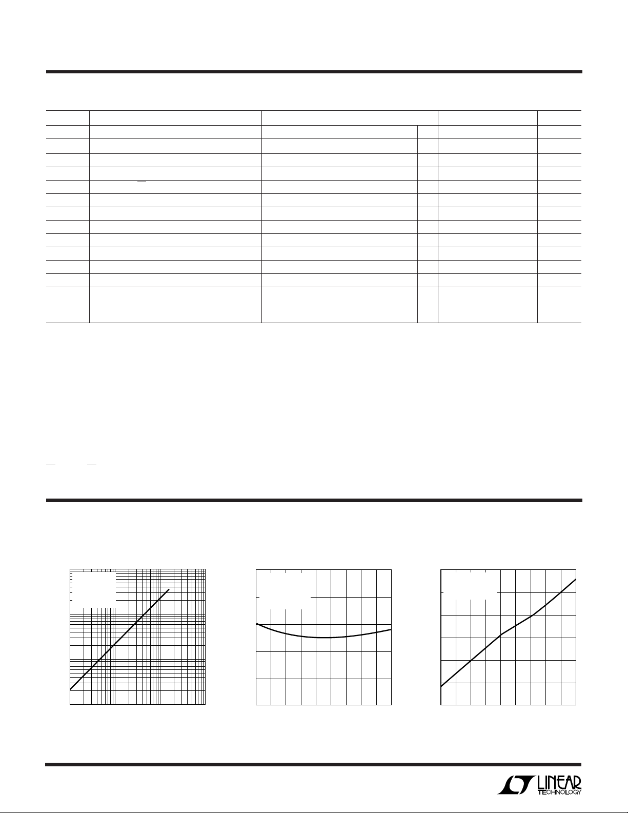
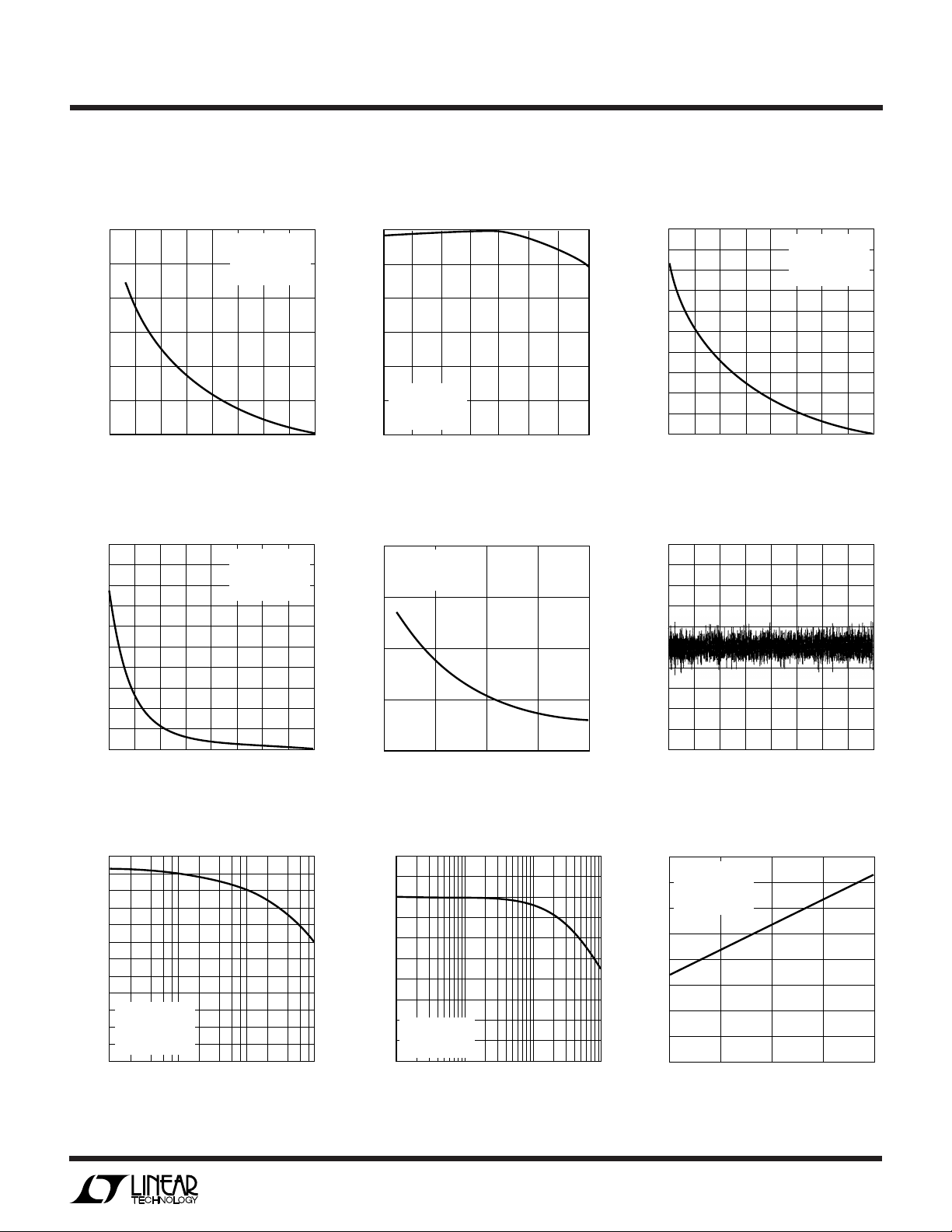
TYPICAL PERFORMANCE CHARACTERISTICS
Supply Current vs Sample Rate
1000
TA = 25°C
= 5V
V
CC
= 5V
V
REF
= 320kHz
f
CLK
100
10
SUPPLY CURRENT (µA)
1
0.1
4
1 10 100
SAMPLE FREQUENCY (kHz)
1594/98 G01
Supply Current vs Temperature
450
TA = 25°C
= V
= 5V
V
CC
REF
= 320kHz
f
CLK
400
350
300
SUPPLY CURRENT (µA)
250
200
f
SMPL
–35 5
–55
= 16.8kHz
–15
TEMPERATURE (°C)
25
85
45 125
105
65
1594/98 G02
Reference Current vs Temperature
Page 5
W
0
–0.05
–0.15
–0.20
–0.25
–0.30
–0.50
–0.35
–0.10
–0.40
–0.45
REFERENCE VOLTAGE (V)
1.0
CHANGE IN LINEARITY (LSB)
2.0 3.0
4.0
5.0
1594/98 G06
1.5 2.5
3.5
4.5
TA = 25°C
V
CC
= 5V
f
CLK
= 320kHz
f
SMPL
= 16.8kHz
INPUT LEVEL (dB)
–40
0
SIGNAL-TO-NOISE PLUS DISTORTION (dB)
20
10
40
30
60
50
80
70
–30 –20
1594/98 G12
–10 0
TA = 25°C
V
CC
= V
REF =
5V
f
IN
= 1kHz
f
SMPL
= 16.8kHz
CODE
0
DIFFERENTIAL NONLINEARITY ERROR (LBS)
–1.0
–0.8
–0.6
–0.4
–0.2
0.4
0.6
0.8
1.0
0.2
0.0
2048
1594/98 G09
4096
U
TYPICAL PERFORMANCE CHARACTERISTICS
LTC1594/LTC1598
Change in Offset
vs Reference Voltage
3.0
)
REF
2.5
2.0
1.5
1.0
0.5
CHANGE IN OFFSET (LSB = 1/4096 V
0
1.0
2.0 3.0
1.5 2.5
REFERENCE VOLTAGE (V)
Change in Gain
vs Reference Voltage
–10
–9
–8
–7
–6
–5
–4
–3
CHANGE IN GAIN (LSB)
–2
–1
0
1.0
2.0 3.0
1.5 2.5
REFERENCE VOLTAGE (V)
TA = 25°C
= 5V
V
CC
= 320kHz
f
CLK
f
SMPL
4.0
3.5
TA = 25°C
= 5V
V
CC
= 320kHz
f
CLK
f
SMPL
4.0
3.5
= 16.8kHz
4.5
1594/98 G04
= 16.8kHz
4.5
1594/98 G07
5.0
5.0
Change in Offset vs Temperature
0
–0.5
–1.0
–1.5
–2.0
CHANGE IN OFFSET (LSB)
–2.5
–3.0
VCC = V
f
f
–55
= 5V
REF
= 320kHz
CLK
= 16.8kHz
SMPL
–15 25
–35 5
TEMPERATURE (°C)
Peak-to-Peak ADC Noise
vs Reference Voltage
2.0
TA = 25°C
V
= 5V
CC
f
= 320kHz
CLK
1.5
1.0
ADC NOISE IN LBSs
0.5
0
1
2
REFERENCE VOLTAGE (V)
3
Change in Linearity
vs Reference Voltage
65
45
85
1594/98 G05
Differential Nonlinearity vs Code
4
5
1594/98 G08
Effective Bits and S/(N + D)
vs Input Frequency
12
11
10
9
8
7
6
5
4
3
TA = 25°C
V
CC
2
f
CLK
EFFECTIVE NUMBER OF BITS (ENOBs)
1
f
SMPL
0
1
= 5V
= 320kHz
= 16.8kHz
10 100 1000
INPUT FREQUENCY (kHz)
1594/98 G10
Spurious Free Dynamic Range
vs Frequency
74
68
62
56
50
44
38
100
90
80
70
60
50
40
30
20
TA = 25°C
= V
V
CC
10
SPURIOUS FREE DYNAMIC RANGE (dB)
f
SMPL
0
1
5V
REF =
= 16.8kHz
10 100 1000
INPUT FREQUENCY (kHz)
1594/98 G11
S/(N + D) vs Input Level
5
Page 6
LTC1594/LTC1598
SOURCE RESISTANCE (Ω)
10 100 1000
1594/98 G18
10.1 10000
100
S & H ACQUISITION TIME (ns)
1000
10000
TA = 25°C
V
CC
= V
REF
= 5V
+INPUT
COM
R
SOURCE
+
V
IN
W
U
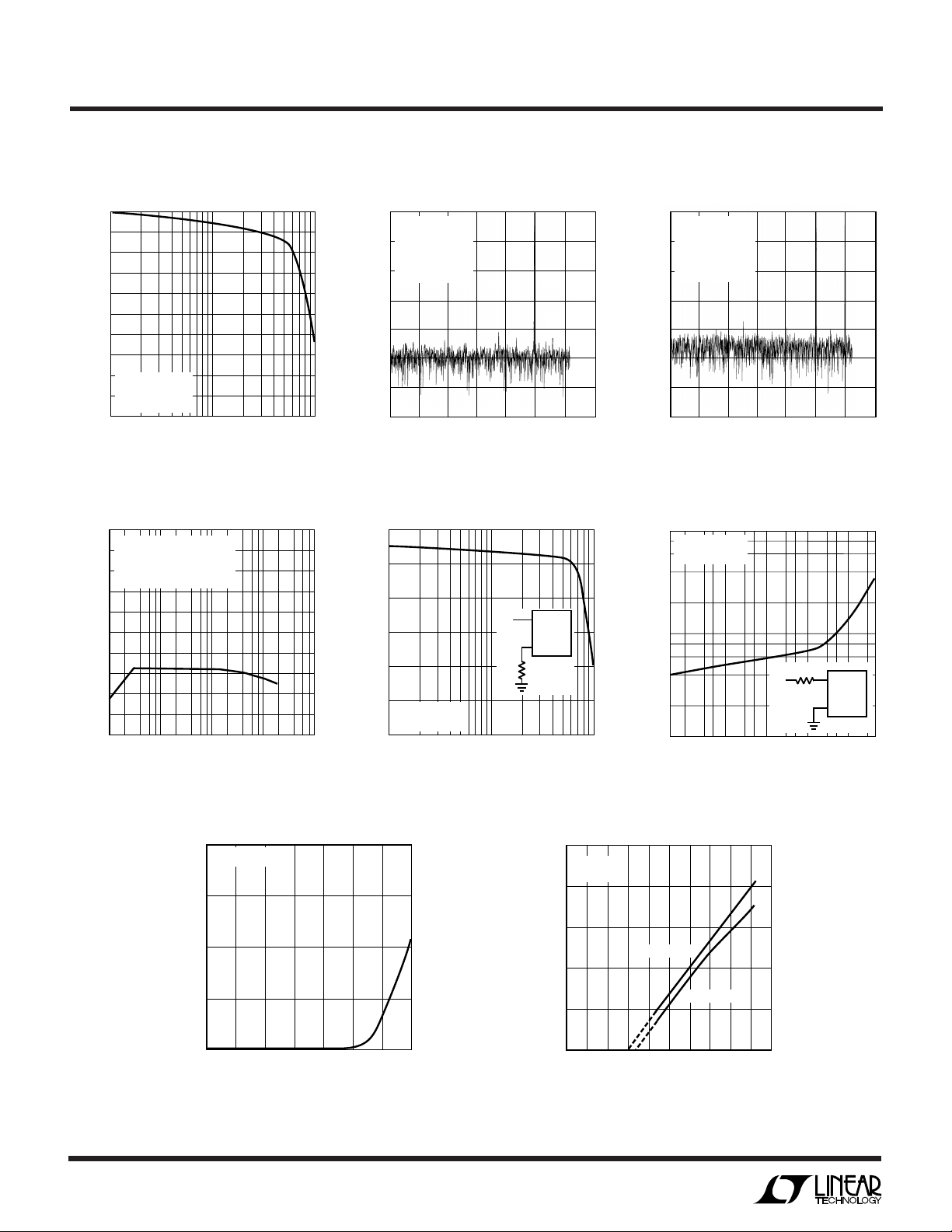
TYPICAL PERFORMANCE CHARACTERISTICS
Attenuation vs Input Frequency
0
10
20
30
40
50
60
ATTENUATION (%)
70
80
TA = 25°C
= V
V
CC
90
f
SMPL
100
110
5V
REF =
= 16.8kHz
INPUT FREQUENCY (kHz)
100 1000 10000
Power Supply Feedthrough
vs Ripple Frequency
0
TA = 25°C
= 5V (V
V
CC
= 5V
V
REF
= 320kHz
f
CLK
–50
FEEDTHROUGH (dB)
–100
1 100 1000 10000
= 20mV)
RIPPLE
10
RIPPLE FREQUENCY (kHz)
1594/98 G13
1594/98 G16
4096 Point FFT Plot
0
TA = 25°C
= V
CC
REF
= 5kHz
IN
= 320kHz
CLK
= 12.5kHz
SMPL
12
= 5V
35
FREQUENCY (kHz)
V
–20
f
f
–40
f
–60
–80
MAGNITUDE (dB)
–100
–120
–140
0
Maximum Clock Frequency
vs Source Resistance
360
300
240
180
120
CLOCK FREQUENCY (kHz)
60
TA = 25°C
= V
V
0
0.1
= 5V
CC
REF
SOURCE RESISTANCE (kΩ)
Intermodulation Distortion
0
TA = 25°C
V
–20
f
1
f
2
–40
f
SMPL
–60
–80
MAGNITUDE (dB)
–100
–120
467
1594/98 G14
–140
0
Sample-and-Hold Acquisition Time
vs Source Resistance
+INPUT
V
IN
COM
–
R
SOURCE
110
1594/98 G17
= V
CC
REF =
= 5kHz
= 6kHz
= 12.5kHz
12
5V
467
35
FREQUENCY (kHz)
1594/98 G15
6
Minimum Clock Frequency for
0.1LSB Error vs Temperature
320
VCC = V
240
160
80
CLOCK FREQUENCY (kHz)
0
–55
–35
REF
–15
= 5V
5
25 45 65 85
TEMPERATURE (°C)
1594/98 G19
Input Channel Leakage Current
vs Temperature
1000
VCC = 5V
V
= 5V
REF
100
10
ON CHANNEL
1
20
OFF CHANNEL
60
40 80
LEAKAGE CURRENT (nA)
0.1
0.01
–60
–40
0
–20
TEMPERATURE (°C)
100
120
1594/98 G20
140
Page 7

UUU
PIN FUNCTIONS
LTC1594
LTC1594/LTC1598
CH0 (Pin 1): Analog Multiplexer Input.
CH1 (Pin 2): Analog Multiplexer Input.
CH2 (Pin 3): Analog Multiplexer Input.
CH3 (Pin 4): Analog Multiplexer Input.
ADCIN (Pin 5): ADC Input. This input is the positive analog
input to the ADC. Connect this pin to MUXOUT for normal
operation.
V
(Pin 6): Reference Input. The reference input defines
REF
the span of the ADC.
COM (Pin 7): Negative Analog Input. This input is the
negative analog input to the ADC and must be free of noise
with respect to GND.
GND (Pin 8): Analog Ground. GND should be tied directly
to an analog ground plane.
CSADC (Pin 9): ADC Chip Select Input. A logic high on this
input powers down the ADC and three-states D
low on this input enables the ADC to sample the selected
channel and start the conversion. For normal operation
drive this pin in parallel with CSMUX.
OUT
. A logic
D
(Pin 10): Digital Data Output. The A/D conversion
OUT
result is shifted out of this output.
VCC (Pin 11): Power Supply Voltage. This pin provides
power to the ADC. It must be bypassed directly to the
analog ground plane.
CLK (Pin 12): Shift Clock. This clock synchronizes the
serial data transfer to both MUX and ADC.
CSMUX (Pin 13): MUX Chip Select Input. A logic high on
this input allows the MUX to receive a channel address. A
logic low enables the selected MUX channel and connects
it to the MUXOUT pin for A/D conversion. For normal
operation, drive this pin in parallel with CSADC.
DIN (Pin 14): Digital Data Input. The multiplexer address
is shifted into this input.
MUXOUT (Pin 15): MUX Output. This pin is the output of
the multiplexer. Tie to ADCIN for normal operation.
VCC (Pin 16): Power Supply Voltage. This pin should be
tied to Pin 11.
LTC1598
CH5 (Pin 1): Analog Multiplexer Input.
CH6 (Pin 2): Analog Multiplexer Input.
CH7 (Pin 3): Analog Multiplexer Input.
GND (Pin 4): Analog Ground. GND should be tied directly
to an analog ground plane.
CLK (Pin 5): Shift Clock. This clock synchronizes the serial
data transfer to both MUX and ADC. It also determines the
conversion speed of the ADC.
CSMUX (Pin 6): MUX Chip Select Input. A logic high on
this input allows the MUX to receive a channel address. A
logic low enables the selected MUX channel and connects
it to the MUXOUT pin for A/D conversion. For normal
operation, drive this pin in parallel with CSADC.
DIN (Pin 7): Digital Data Input. The multiplexer address is
shifted into this input.
COM (Pin 8): Negative Analog Input. This input is the
negative analog input to the ADC and must be free of noise
with respect to GND.
GND (Pin 9): Analog Ground. GND should be tied directly
to an analog ground plane.
CSADC (Pin 10): ADC Chip Select Input. A logic high on
this input deselects and powers down the ADC and threestates D
sample the selected channel and start the conversion. For
normal operation drive this pin in parallel with CSMUX.
D
OUT
result is shifted out of this output.
NC (Pin 12): No Connection.
NC (Pin 13): No Connection.
CLK (Pin 14): Shift Clock. This input should be tied to Pin 5.
. A logic low on this input enables the ADC to
OUT
(Pin 11): Digital Data Output. The A/D conversion
7
Page 8
LTC1594/LTC1598
UUU
PIN FUNCTIONS
VCC (Pin 15): Power Supply Voltage. This pin provides
power to the A/D Converter. It must be bypassed directly
to the analog ground plane.
V
(Pin 16): Reference Input. The reference input de-
REF
fines the span of the ADC.
ADCIN (Pin 17): ADC Input. This input is the positive
analog input to the ADC. Connect this pin to MUXOUT for
normal operation.
MUXOUT (Pin 18): MUX Output. This pin is the output of
the multiplexer. Tie to ADCIN for normal operation.
W
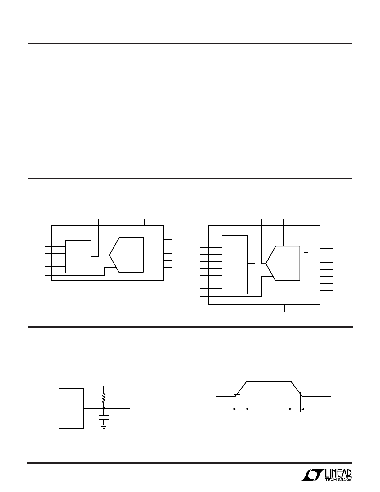
BLOCK DIAGRA S
LTC1594
15 5 6 16
+
SAMPLING
–
V
12-BIT
ADC
GND
REFVCC
8
CSADC
CSMUX
CLK
D
D
OUT
LTC1594
9
13
12
14
IN
10
1
CH0
2
CH1
3
CH2
4
CH3
7 COM
ADCINMUXOUT
4-CHANNEL
MUX
VCC (Pin 19): Power Supply Voltage. This pin should be
tied to Pin 15.
CH0 (Pin 20): Analog Multiplexer Input.
CH1 (Pin 21): Analog Multiplexer Input.
CH2 (Pin 22): Analog Multiplexer Input.
CH3 (Pin 23): Analog Multiplexer Input.
CH4 (Pin 24): Analog Multiplexer Input.
LTC1598
18 17 16 15, 19
+
SAMPLING
–
V
12-BIT
ADC
GND
REFVCC
4, 9
CSADC
CSMUX
CLK
D
D
OUT
NC
NC
LTC1598
1594/98 BD
10
6
5, 14
7
IN
11
12
13
20
21
22
23
24
1
2
3
8 COM
CH0
CH1
CH2
CH3
CH4
CH5
CH6
CH7
ADCINMUXOUT
8-CHANNEL
MUX
TEST CIRCUITS
Load Circuit for t
D
OUT
8
1.4V
3k
dDO
100pF
, tr and t
TEST POINT
f
1594/98 TC01
Voltage Waveforms for D
D
OUT
t
r
Rise and Fall Times, tr, t
OUT
t
f
1594/98 TC02
f
V
OH
V
OL
Page 9

TEST CIRCUITS
LTC1594/LTC1598
Voltage Waveforms for D
CLK
D
OUT
V
IL
t
dDO
Load Circuit for t
TEST POINT
D
OUT
3k
100pF
Delay Times, t
OUT
and t
dis
en
VCC t
dis
t
WAVEFORM 1
dis
dDO
V
OH
V
OL
1594/98 TC03
WAVEFORM 2, t
1594/98 TC04
Voltage Waveforms for t
LTC1594/LTC1598
CSADC
CLK
D
OUT
1
Voltage Waveforms for t
CSADC = CSMUX = CS
en
D
OUT
WAVEFORM 1
(SEE NOTE 1)
D
OUT
WAVEFORM 2
(SEE NOTE 2)
NOTE 1: WAVEFORM 1 IS FOR AN OUTPUT WITH INTERNAL CONDITIONS SUCH
THAT THE OUTPUT IS HIGH UNLESS DISABLED BY THE OUTPUT CONTROL.
NOTE 2: WAVEFORM 2 IS FOR AN OUTPUT WITH INTERNAL CONDITIONS SUCH
THAT THE OUTPUT IS LOW UNLESS DISABLED BY THE OUTPUT CONTROL.
en
2
B11
V
OL
t
en
1594/98 TC06
dis
V
IH
90%
t
dis
10%
1594/98 TC05
9
Page 10

LTC1594/LTC1598
U
WUU
APPLICATIONS INFORMATION
OVERVIEW
The LTC1594/LTC1598 are micropower, 12-bit sampling
A/D converters that feature a 4- and 8-channel multiplexer respectively. They typically draw only 320µA of
supply current when sampling at 16.8kHz. Supply current drops linearly as the sample rate is reduced (see
Supply Current vs Sample Rate). The ADCs automatically
power down when not performing conversions, drawing
only leakage current. The LTC1594 is available in a 16-pin
narrow SO package and the LTC1598 is packaged in a
24-pin SSOP. Both devices operate on a single supply
from 4.5V to 5.5V.
The LTC1594/LTC1598 contain a 12-bit, switchedcapacitor ADC, sample-and-hold, serial port and an
external reference input pin. In addition, the LTC1594 has
a 4-channel multiplexer and the LTC1598 provides an
8-channel multiplexer (see Block Diagram). They can
measure signals floating on a DC common mode voltage
and can operate with reduced spans to 1.5V. Reducing
the spans allow them to achieve 366µV resolution.
The LTC1594/LTC1598 provide separate MUX output
and ADC input pins to form an ideal MUXOUT/ADCIN
loop which economizes signal conditioning. The MUX
and ADC of the devices can also be controlled individually
through separate chip selects to enhance flexibility.
SERIAL INTERFACE
For this discussion we will assume that CSMUX and
CSADC are tied together and will refer to them as simply
CS, unless otherwise specified.
The LTC1594/LTC1598 communicate with the microprocessor and other external circuitry via a synchronous,
half duplex, 4-wire interface (see Operating Sequences in
Figures 1 and 2).
t
CYC
CSMUX = CSADC = CS
t
suCS
CLK
EN D1
D
IN
Hi-Z
D0
THE ADC WILL OUTPUT LSB-FIRST DATA THEN FOLLOWED WITH ZEROS INDEFINITELY
t
SMPL
NULL
BIT
t
ON
D2
D
OUT
CH0 TO
CH7
ADCIN =
MUXOUT
COM = GND *AFTER COMPLETING THE DATA TRANSFER, IF FURTHER CLOCKS ARE APPLIED WITH CS LOW,
DON’T CARE
B2 B1 B0*
B6
B8B9
B10B11
B7
t
CONV
B5
B3
B4
Figure 1. LTC1594/LTC1598 Operating Sequence Example: CH2, GND
Hi-Z
1594/98 F01
10
Page 11

LTC1594/LTC1598
D
IN1
D
IN2
D
OUT1
D
OUT2
CS
SHIFT MUX
ADDRESS IN
t
SMPL
+ 1 NULL BIT
SHIFT A/D CONVERSION
RESULT OUT
1594/98 AI01
U
WUU
APPLICATIONS INFORMATION
CSMUX = CSADC = CS
t
suCS
CLK
EN D1
D
IN
D0
D2
D
OUT
CH0 TO
CH7
ADCIN =
MUXOUT
COM = GND
Figure 2. LTC1594/LTC1598 Operating Sequence Example: All Channels Off
Hi-Z
t
OFF
NULL
BIT
t
CYC
D0N‘T CARE
DUMMY CONVERSION
t
CONV
Hi-Z
1594/98 F02
Data Transfer
The CLK synchronizes the data transfer with each bit
being transmitted on the falling CLK edge and captured
on the rising CLK edge in both transmitting and receiving
systems.
The LTC1594/LTC1598 first receive input data and then
transmit back the A/D conversion results (half duplex).
Because of the half duplex operation, DIN and D
OUT
may
be tied together allowing transmission over just 3 wires:
CS, CLK and DATA (DIN/D
OUT
).
Data transfer is initiated by a rising chip select (CS)
signal. After CS rises the input data on the DIN pin is
latched into a 4-bit register on the rising edge of the clock.
More than four input bits can be sent to the DIN pin
without problems, but only the last four bits clocked in
before CS falls will be stored into the 4-bit register. This
4-bit input data word will select the channel in the
muliplexer (see Input Data Word and Tables 1 and 2). To
ensure correct operation the CS must be pulled low
before the next rising edge of the clock.
Once the CS is pulled low, all channels are simultaneously switched off after a delay of t
to ensure a
OFF
break-before-make interval, t
(t
OFF
+ t
), the selected channel is switched on,
OPEN
. After a delay of t
OPEN
ON
allowing the ADC in the chip to acquire input signal and
start the conversion (see Figures 1 and 2). After 1 null bit,
the result of the conversion is output on the D
OUT
line.
The selected channel remains on, until the next falling
edge of CS. At the end of the data exchange CS should be
brought high. This resets the LTC1594/LTC1598 and
initiates the next data exchange.
Break-Before-Make
The LTC1594/LTC1598 provide a break-before-make
interval from switching off all the channels simultaneously to switching on the next selected channel once
CS is pulled low. In other words, once CS is pulled low,
11
Page 12

LTC1594/LTC1598
U
WUU
APPLICATIONS INFORMATION
after a delay of t
ensure a break-before-make interval. After this interval,
the selected channel is switched on allowing signal
transmission. The selected channel remains on until the
next falling edge of CS and the process repeats itself with
the “EN” bit being logic high. If the “EN” bit is logic low,
all the channels are switched off simultaneously after a
delay of t
OFF
channels remain off until the next falling edge of CS.
Input Data Word
When CS is high, the LTC1594/LTC1598 clock data into
the DIN inputs on the rising edge of the clock and store the
data into a 4-bit register. The input data words are defined
as follows:
, all the channels are switched off to
OFF
from CS being pulled low and all the
D0EN D2 D1
CHANNEL SELECTION
1594/98 AI02
Table 2. Logic Table for the LTC1598 Channel Selection
CHANNEL STATUS EN D2 D1 DO
All Off 0 X X X
CH0 1 0 0 0
CH1 1 0 0 1
CH2 1 0 1 0
CH3 1 0 1 1
CH4 1 1 0 0
CH5 1 1 0 1
CH6 1 1 1 0
CH7 1 1 1 1
Transfer Curve
The LTC1594/LTC1598 are permanently configured for
unipolar only. The input span and code assignment for
this conversion type is illustrated below.
Transfer Curve
“EN” Bit
The first bit in the 4-bit register is an “EN” bit. If the “EN”
bit is a logic high, as illustrated in Figure 1, it enables the
selected channel after a delay of tON when the CS is pulled
low. If the “EN” bit is logic low, as illustrated in Figure 2,
it disables all channels after a delay of t
when the CS
OFF
is pulled low.
Multiplexer (MUX) Address
The 3 bits of input word following the “EN” bit select the
channel in the MUX for the requested conversion. For a
given channel selection, the converter will measure the
voltage of the selected channel with respect to the voltage
on the COM pin. Tables 1 and 2 show the various bit
combinations for the LTC1594/LTC1598 channel selection.
Table 1. Logic Table for the LTC1594 Channel Selection
CHANNEL STATUS EN D2 D1 DO
All Off 0 X X X
CH0 1 0 0 0
CH1 1 0 0 1
CH2 1 0 1 0
CH3 1 0 1 1
1 1 1 1 1 1 1 1 1 1 1 1
1 1 1 1 1 1 1 1 1 1 1 0
•
•
•
0 0 0 0 0 0 0 0 0 0 0 1
0 0 0 0 0 0 0 0 0 0 0 0
OUTPUT CODE
1 1 1 1 1 1 1 1 1 1 1 1 1 1
1 1 1 1 1 1 1 1 1 1 1 1 1 0
0 0 0 0 0 0 0 0 0 0 0 0 0 1
0 0 0 0 0 0 0 0 0 0 0 0 0 0
V
IN
0V
1LSB
1LSB =
V
REF
4096
V
REF
–2LSB
V
REF
–1LSB
V
REF
1594/98 • AI03
Output Code
INPUT VOLTAGE
•
•
•
V
V
REF
REF
– 1LSB
– 2LSB
•
•
•
1LSB
0V
INPUT VOLTAGE
(V
= 5.000V)
REF
4.99878V
4.99756V
•
•
•
0.00122V
0V
1594/98 • AI04
12
Page 13

LTC1594/LTC1598
U
WUU
APPLICATIONS INFORMATION
Operation with DIN and D
The LTC1594/LTC1598 can be operated with DIN and
D
tied together. This eliminates one of the lines
OUT
required to communicate to the microprocessor (MPU).
Data is transmitted in both directions on a single wire.
The processor pin connected to this data line should be
configurable as either an input or an output. The LTC1594/
LTC1598 will take control of the data line after CS falling
and before the 6th falling CLK while the processor takes
control of the data line when CS is high (see Figure 3).
CS
CLK
Tied Together
OUT
1
2 3 456
Therefore the processor port line must be switched to an
input with CS being low to avoid a conflict.
Separate Chip Selects for MUX and ADC
The LTC1594/LTC1598 provide separate chip selects,
CSMUX and CSADC, to control MUX and ADC separately.
This feature not only provides the flexibility to select a
particular channel once for multiple conversions (see
Figure 4) but also maximizes the sample rate up to
20ksps (see Figure 5).
t
suCS
DATA (D
CSMUX
CSADC
CLK
D
OUT
CH0 TO
CH7
ADCIN =
MUXOUT
COM = GND
IN/DOUT
D
IN
)
EN D1
EN D2 D1 D0 B11 B10
MPU CONTROLS DATA LINE AND SENDS
MUX ADDRESS TO LTC1594/LTC1598
PROCESSOR MUST RELEASE DATA
LINE AFTER CS FALLING AND
BEFORE THE 6TH FALLING CLK
Figure 3. LTC1594/LTC1598 Operation with DIN and D
t
suCS
D0
D2
Hi-Z
t
SMPL
t
NULL
BIT
ON
DON’T CARE
B2 B1 B0
B6
B8B9
B10B11
B7
t
CONV
B3
B4
B5
t
suCS
D0
Hi-Z
t
SMPL
NULL
BIT
Tied Together
OUT
B10B11
LTC1594/LTC1598 CONTROLS DATA LINE AND SENDS
LTC1594/LTC1598 TAKES CONTROL OF DATA
LINE AFTER CS FALLING AND BEFORE THE
6TH FALLING CLK
DON’T CARE
B8B9
B7
t
CONV
A/D RESULT BACK TO MPU
B6
B4
B5
B3
B2 B1 B0
•••
1594/98 F03
Hi-Z
1594 TD01
Figure 4. Select Certain Channel Once for Mulitple Conversions
13
Page 14

LTC1594/LTC1598
U
WUU
APPLICATIONS INFORMATION
CSADC
CSMUX
t
CLK
EN D1
D2
B2 B1 B0
B3
B4
D
OUT
CH0 TO
CH7
ADCIN =
MUXOUT
COM = GND
D
IN
MUXOUT/ADCIN Loop Economizes
Signal Conditioning
The MUXOUT and ADCIN pins of the LTC1594/LTC1598
form a very flexible external loop that allows Programmable Gain Amplifier (PGA) and/or processing analog
input signals prior to conversion. This loop is also a cost
effective way to perform the conditioning, because only
one circuit is needed instead of one for each channel.
suCS
D0
t
SMPL
t
NULL
BIT
ON
DON’T CARE DON’T CARE
B6
B8B9
B10B11
B7
t
CONV
B3
B5
B4
Figure 5. Use Separate Chip Selects to Maximize Sample Rate
EN D1
B2 B1 B0
t
suCS
EN D1
D0D2
1000
100
SUPPLY CURRENT (µA)
t
10
SMPL
t
ON
TA = 25°C
V
V
f
CLK
NULL
BIT
= 5V
CC
= 5V
REF
= 320kHz
B2 B1 B0
B6
B8B9
B10B11
B7
t
CONV
B3
B5
B4
D0D2
1594/98 F05
In the Typical Applications section, there are a few
examples illustrating how to use the MUXOUT/ADCIN loop
to form a PGA and to antialias filter several analog inputs.
ACHIEVING MICROPOWER PERFORMANCE
With typical operating currents of 320µA and automatic
shutdown between conversions, the LTC1594/LTC1598
achieve extremely low power consumption over a wide
range of sample rates (see Figure 6). The auto shutdown
allows the supply current to drop with reduced sample
rate. Several things must be taken into account to achieve
such a low power consumption.
Shutdown
The LTC1594/LTC1598 are equipped with automatic shutdown features. They draw power when the CS pin is low.
The bias circuits and comparator of the ADC powers down
and the reference input becomes high impedance at the
end of each conversion leaving the CLK running to clock
out the LSB first data or zeroes (see Figures 1 and 2). When
the CS pin is high, the ADC powers down completely
1
0.1
1 10 100
SAMPLE FREQUENCY (kHz)
1594/98 F06
Figure 6. Automatic Power Shutdown Between Conversions
Allows Power Consumption to Drop with Sample Rate
leaving the CLK running to clock the input data word into
MUX. If the CS, DIN and CLK are not running rail-to-rail, the
input logic buffers will draw currents. These currents may
be large compared to the typical supply current. To obtain
the lowest supply current, run the CS, DIN and CLK pins
rail-to-rail.
D
Loading
OUT
Capacitive loading on the digital output can increase
power consumption. A 100pF capacitor on the D
OUT
pin
can add more than 80mA to the supply current at a
320kHz clock frequency. An extra 80mA or so of current
goes into charging and discharging the load capacitor.
The same goes for digital lines driven at a high frequency
by any logic. The (C)(V)(f) currents must be evaluated
and the troublesome ones minimized.
14
Page 15

LTC1594/LTC1598
U
WUU
APPLICATIONS INFORMATION
BOARD LAYOUT CONSIDERATIONS
Grounding and Bypassing
The LTC1594/LTC1598 are easy to use if some care is
taken. They should be used with an analog ground plane
and single point grounding techniques. The GND pin
should be tied directly to the ground plane.
The VCC pin should be bypassed to the ground plane with
a 10µF tantalum capacitor with leads as short as possible.
If the power supply is clean, the LTC1594/LTC1598 can
also operate with smaller 1µF or less surface mount or
ceramic bypass capacitors. All analog inputs should be
referenced directly to the single point ground. Digital
inputs and outputs should be shielded from and/or
routed away from the reference and analog circuitry.
CSADC = CSMUX = CS
SAMPLE-AND-HOLD
Both the LTC1594/LTC1598 provide a built-in sampleand-hold (S&H) function to acquire signals through the
selected channel, assuming the ADCIN and MUXOUT
pins are tied together. The S & H of these parts acquire
input signals through the selected channel relative to
COM input during the t
time (see Figure 7).
SMPL
Single-Ended Inputs
The sample-and-hold of the LTC1594/LTC1598 allows
conversion of rapidly varying signals. The input voltage
is sampled during the t
time as shown in Figure 7.
SMPL
The sampling interval begins after tON time once the CS
is pulled low and continues until the second falling CLK
edge after the CS is low (see Figure 7). On this falling CLK
SAMPLE HOLD
t
ON
“ANALOG” INPUT MUST
SETTLE DURING
THIS TIME
t
SMPL
t
CONV
CLK
D
D
OUT
MUXOUT = ADCIN
CH0 TO CH7
COM
IN
Figure 7. LTC1594/LTC1598 ADCIN and COM Input Settling Windows
D2 D1EN D0
1ST BIT TEST “COM” INPUT MUST
SETTLE DURING THIS TIME
DON‘T CARE
B11
1594/98 F07
15
Page 16

LTC1594/LTC1598
U
WUU
APPLICATIONS INFORMATION
edge, the S & H goes into hold mode and the conversion
begins. The voltage on the “COM” input must remain
constant and be free of noise and ripple throughout the
conversion time. Otherwise, the conversion operation
may not be performed accurately. The conversion time is
12 CLK cycles. Therefore, a change in the “COM” input
voltage during this interval can cause conversion errors.
For a sinusoidal voltage on the “COM” input this error
would be:
V
ERROR(MAX)
Where f(“COM”) is the frequency of the “COM” input
voltage, V
frequency of the CLK. In most cases V
significant. For a 60Hz signal on the “COM” input to
generate a 1/4LSB error (305µV) with the converter
running at CLK = 320kHz, its peak value would have to be
8.425mV.
ANALOG INPUTS
= V
is its peak amplitude and f
PEAK
(2π)(f)(“COM”)12/f
PEAK
ERROR
CLK
is the
CLK
will not be
During the conversion, the “analog” input voltage is
effectively “held” by the sample-and-hold and will not
affect the conversion result. However, it is critical that the
“COM” input voltage settles completely during the first
CLK cycle of the conversion time and be free of noise.
Minimizing R
SOURCE
–
and C2 will improve settling time.
If a large “COM” input source resistance must be used,
the time allowed for settling can be extended by using a
slower CLK frequency.
Input Op Amps
When driving the analog inputs with an op amp it is
important that the op amp settle within the allowed time
(see Figure 7). Again, the “analog” and “COM” input
sampling times can be extended as described above to
accommodate slower op amps. Most op amps, including
the LT®1006 and LT1413 single supply op amps, can be
made to settle well even with the minimum settling
windows of 4.8µs (“analog” input) which occur at the
maximum clock rate of 320kHz.
Because of the capacitive redistribution A/D conversion
techniques used, the analog inputs of the LTC1594/
LTC1598 have capacitive switching input current spikes.
These current spikes settle quickly and do not cause a
problem. However, if large source resistances are used
or if slow settling op amps drive the inputs, care must be
taken to insure that the transients caused by the current
spikes settle completely before the conversion begins.
“Analog” Input Settling
The input capacitor of the LTC1594/LTC1598 is switched
onto the selected channel input during the t
SMPL
time (see
Figure 7) and samples the input signal within that time. The
sample phase is at least 1 1/2 CLK cycles before conversion starts. The voltage on the “analog” input must settle
completely within t
. Minimizing R
SMPL
SOURCE
+
and C1 will
improve the input settling time. If a large “analog” input
source resistance must be used, the sample time can be
increased by using a slower CLK frequency.
“COM” Input Settling
At the end of the t
, the input capacitor switches to the
SMPL
“COM” input and conversion starts (see Figures 1 and 7).
Source Resistance
The analog inputs of the LTC1594/LTC1598 look like a
20pF capacitor (CIN) in series with a 500Ω resistor (RON)
and a 45Ω channel resistance as shown in Figure 8.
CIN gets switched between the selected “analog” and
“COM” inputs once during each conversion cycle. Large
external source resistors and capacitances will slow the
settling of the inputs. It is important that the overall RC
time constants be short enough to allow the analog
inputs to completely settle within the allowed time.
MUX
VIN+
“ANALOG”
INPUT
+
R
SOURCE
Figure 8. Analog Input Equivalent Circuit
C1
VIN–
R
45Ω
ON
R
SOURCE
MUXOUT
ADCIN
“COM”
INPUT
–
C2
R
ON
500Ω
LTC1594
LTC1598
C
IN
20pF
1594/98 • F08
16
Page 17

LTC1594/LTC1598
U
WUU
APPLICATIONS INFORMATION
Input Leakage Current
Input leakage currents can also create errors if the source
resistance gets too large. For instance, the maximum
input leakage specification of 200nA (at 85°C) flowing
through a source resistance of 1.2k will cause a voltage
drop of 240µV or 0.2LSB. This error will be much
reduced at lower temperatures because leakage drops
rapidly (see typical curve Input Channel Leakage Current
vs Temperature).
REFERENCE INPUTS
The reference input of the LTC1594/LTC1598 is effectively a 50k resistor from the time CS goes low to the end
of the conversion. The reference input becomes a high
impedance node at any other time (see Figure 9). Since
the voltage on the reference input defines the voltage
span of the A/D converter, the reference input should be
driven by a reference with low R
and LT1021) or a voltage source with low R
+
REF
1
R
OUT
V
REF
GND
4
Figure 9. Reference Input Equivalent Circuit
Reduced Reference Operation
The effective resolution of the LTC1594/LTC1598 can be
increased by reducing the input span of the converters.
The LTC1594/LTC1598 exhibit good linearity and gain
over a wide range of reference voltages (see typical
curves Change in Linearity vs Reference Voltage and
Change in Gain vs Reference Voltage). However, care
must be taken when operating at low values of V
because of the reduced LSB step size and the resulting
higher accuracy requirement placed on the converters.
The following factors must be considered when operating at low V
values:
REF
1. Offset
2. Noise
3. Conversion speed (CLK frequency)
(ex. LT1004, LT1019
OUT
OUT
LTC1594
LTC1598
1594/98 F09
.
REF
Offset with Reduced V
REF
The offset of the LTC1594/LTC1598 has a larger effect on
the output code when the ADCs are operated with
reduced reference voltage. The offset (which is typically
a fixed voltage) becomes a larger fraction of an LSB as the
size of the LSB is reduced. The typical curve of Change in
Offset vs Reference Voltage shows how offset in LSBs is
related to reference voltage for a typical value of VOS. For
example, a VOS of 122µV which is 0.1LSB with a 5V
reference becomes 0.5LSB with a 1V reference and
2.5LSBs with a 0.2V reference. If this offset is unacceptable, it can be corrected digitally by the receiving system
or by offsetting the “COM” input of the LTC1594/LTC1598.
Noise with Reduced V
REF
The total input referred noise of the LTC1594/LTC1598
can be reduced to approximately 400µV peak-to-peak
using a ground plane, good bypassing, good layout
techniques and minimizing noise on the reference inputs.
This noise is insignificant with a 5V reference but will
become a larger fraction of an LSB as the size of the LSB
is reduced.
For operation with a 5V reference, the 400µV noise is only
0.33LSB peak-to-peak. In this case, the LTC1594/LTC1598
noise will contribute virtually no uncertainty to the output
code. However, for reduced references the noise may
become a significant fraction of an LSB and cause
undesirable jitter in the output code. For example, with a
2.5V reference this same 400µV noise is 0.66LSB peak-
to-peak. This will reduce the range of input voltages over
which a stable output code can be achieved by 1LSB. If
the reference is further reduced to 1V, the 400µV noise
becomes equal to 1.65LSBs and a stable code may be
difficult to achieve. In this case averaging multiple readings may be necessary.
This noise data was taken in a very clean setup. Any setup
induced noise (noise or ripple on VCC, V
or VIN) will
REF
add to the internal noise. The lower the reference voltage
to be used the more critical it becomes to have a clean,
noise free setup.
17
Page 18

LTC1594/LTC1598
U
WUU
APPLICATIONS INFORMATION
Conversion Speed with Reduced V
With reduced reference voltages, the LSB step size is
reduced and the LTC1594/LTC1598 internal comparator
overdrive is reduced. Therefore, it may be necessary to
reduce the maximum CLK frequency when low values of
V
are used.
REF
DYNAMIC PERFORMANCE
The LTC1594/LTC1598 have exceptional sampling capability. Fast Fourier Transform (FFT) test techniques are
used to characterize the ADC’s frequency response,
distortion and noise at the rated throughput. By applying
a low distortion sine wave and analyzing the digital
output using an FFT algorithm, the ADC’s spectral content can be examined for frequencies outside the fundamental. Figure 10 shows a typical LTC1594/LTC1598
plot.
0
TA = 25°C
= V
CC
= 5kHz
IN
CLK
SMPL
= 5V
REF
= 320kHz
= 12.5kHz
V
–20
f
f
–40
f
–60
–80
MAGNITUDE (dB)
–100
–120
REF
Effective Number of Bits
The Effective Number of Bits (ENOBs) is a measurement of
the resolution of an ADC and is directly related to S/(N + D)
by the equation:
ENOB = [S/(N + D) – 1.76]/6.02
where S/(N + D) is expressed in dB. At the maximum
sampling rate of 16.8kHz with a 5V supply, the LTC1594/
LTC1598 maintain above 11 ENOBs at 10kHz input
frequency. Above 10kHz the ENOBs gradually decline, as
shown in Figure 11, due to increasing second harmonic
distortion. The noise floor remains low.
12
11
10
9
8
7
6
5
4
3
TA = 25°C
= 5V
V
CC
2
= 320kHz
f
CLK
EFFECTIVE NUMBER OF BITS (ENOBs)
1
= 16.8kHz
f
SMPL
0
1
10 100 1000
INPUT FREQUENCY (kHz)
Figure 11. Effective Bits and S/(N + D) vs Input Frequency
74
68
62
56
50
44
38
1594/98 G10
–140
0
12
FREQUENCY (kHz)
467
35
1594/98 G14
Figure 10. LTC1594/LTC1598 Nonaveraged, 4096 Point FFT Plot
Signal-to-Noise Ratio
The Signal-to-Noise plus Distortion Ratio (S/N + D) is the
ratio between the RMS amplitude of the fundamental
input frequency to the RMS amplitude of all other frequency components at the ADC’s output. The output is
band limited to frequencies above DC and below one half
the sampling frequency. Figure 11 shows a typical spectral content with a 16.8kHz sampling rate.
18
Total Harmonic Distortion
Total Harmonic Distortion (THD) is the ratio of the RMS
sum of all harmonics of the input signal to the fundamental itself. The out-of-band harmonics alias into the frequency band between DC and half of the sampling
frequency. THD is defined as:
THD =
20log
++++
VVV V
22324
2
V
1
...
2
N
where V1 is the RMS amplitude of the fundamental
frequency and V2 through VN are the amplitudes of the
second through the Nth harmonics. The typical THD
Page 19

LTC1594/LTC1598
U
WUU
APPLICATIONS INFORMATION
specification in the Dynamic Accuracy table includes the
2nd through 5th harmonics. With a 7kHz input signal, the
LTC1594/LTC1598 have typical THD of 80dB with VCC = 5V.
Intermodulation Distortion
If the ADC input signal consists of more than one
spectral component, the ADC transfer function nonlinearity can produce intermodulation distortion (IMD)
in addition to THD. IMD is the change in one sinusoidal input caused by the presence of another sinusoidal
input at a different frequency.
If two pure sine waves of frequencies fa and fb are applied
to the ADC input, nonlinearities in the ADC transfer
function can create distortion products at sum and
difference frequencies of mfa ± nfb, where m and n = 0,
1, 2, 3, etc. For example, the 2nd order IMD terms include
(fa + fb) and (fa – fb) while 3rd order IMD terms include
(2fa + fb), (2fa – fb), (fa + 2fb), and (fa – 2fb). If the two input
sine waves are equal in magnitudes, the value (in dB) of
the 2nd order IMD products can be expressed by the
following formula:
For input frequencies of 5kHz and 6kHz, the IMD of the
LTC1594/LTC1598 is 73dB with a 5V supply.
Peak Harmonic or Spurious Noise
The peak harmonic or spurious noise is the largest
spectral component excluding the input signal and DC.
This value is expressed in dBs relative to the RMS value
of a full-scale input signal.
Full-Power and Full-Linear Bandwidth
The full-power bandwidth is that input frequency at which
the amplitude of the reconstructed fundamental is reduced by 3dB for a full-scale input.
The full-linear bandwidth is the input frequency at which
the effective bits rating of the ADC falls to 11 bits. Beyond
this frequency, distortion of the sampled input signal
increases. The LTC1594/LTC1598 have been designed to
optimize input bandwidth, allowing the ADCs to
undersample input signals with frequencies above the
converters’ Nyquist Frequency.
IMD f f
±
()
ab
20log
=
a
mplitude f f
amplitude at f
()
±
ab
a
U
TYPICAL APPLICATIONS N
Microprocessor Interfaces
The LTC1594/LTC1598 can interface directly (without
external hardware) to most popular microprocessors’
(MPU) synchronous serial formats including
MICROWIRE, SPI and QSPI. If an MPU without a dedicated serial port is used, then three of the MPU’s parallel
port lines can be programmed to form the serial link to the
LTC1594/LTC1598. Included here is one serial interface
example.
Motorola SPI (MC68HC05)
The MC68HC05 has been chosen as an example of an MPU
with a dedicated serial port. This MPU transfers data MSBfirst and in 8-bit increments. The DIN word sent to the data
register starts the SPI process. With three
8-bit transfers the A/D result is read into the MPU. The
second 8-bit transfer clocks B11 through B7 of the A/D
conversion result into the processor. The third 8-bit transfer clocks the remaining bits B6 through B0 into the MPU.
ANDing the second byte with 1F
significant bits and ANDing the third byte with FE
the least significant bit. Shifting the data to the right by one
bit results in a right justified word.
clears the three most
HEX
HEX
clears
19
Page 20

LTC1594/LTC1598
U
TYPICAL APPLICATIONS N
MC68HC05 CODE
LDA #$52 Configuration data for serial peripheral
control register (Interrupts disabled, output
STA $0A Load configuration data into location $0A (SPCR)
LDA #$FF Configuration data for I/O ports
STA $04 Load configuration data into Port A DDR ($04)
STA $05 Load configuration data into Port B DDR ($05)
STA $06 Load configuration data into Port C DDR ($06)
LDA #$08 Put D
STA $50 Load D
START BSET 0,$02 Bit 0 Port C ($02) goes high (CS goes high)
LDA $50 Load D
STA $0C Load D
LOOP1 TST $0B Test status of SPIF bit in SPI status register ($0B)
enabled, master, Norm = 0, Ph = 0, Clk/16)
(all bits are set as outputs)
word for LTC1598 into Accumulator
IN
(CH0 with respect to GND)
word into memory location $50
IN
word at $50 into Accumulator
IN
word into SPI data register ($0C) and
IN
start clocking data
Data Exchange Between LTC1598 and MC68HC05
BPL LOOP1 Loop if not done with transfer to previous instruction
BCLR 0,$02 Bit 0 Port C ($02) goes low (CS goes low)
LDA $0C Load contents of SPI data register into Accumulator
STA $0C Start next SPI cycle
LOOP2 TST $0B Test status of SPIF
BPL LOOP2 Loop if not done
LDA $0C Load contents of SPI data register into Accumulator
STA $0C Start next SPI cycle
AND #$IF Clear 3 MSBs of first D
OUT
word
STA $00 Load Port A ($00) with MSBs
LOOP3 TST $0B Test status of SPIF
BPL LOOP3 Loop if not done
LDA $0C Load contents of SPI data register into Accumulator
AND #$FE Clear LSB of second D
OUT
word
STA $01 Load Port B ($01) with LSBs
JMP START Go back to start and repeat program
CSMUX
= CSADC
= CS
CLK
D
D
OUT
MPU
TRANSMIT
WORD
MPU
RECEIVED
WORD
IN
000
EN
EN D20D1
BYTE 1
???
BYTE 1
DO
D1D2
D0
?????
X
?
?
X
BYTE 2
B11
0
BYTE 2
X
X
B10
X
X
B9
X
B8
DON‘T CARE
X
B7
B3B7 B6 B5 B4 B2 B1 B0 B1 B2B11 B10 B9 B8
X
X
B6
XX
X
BYTE 3
B5
B4 B2
B3
BYTE 3
X
X
X
B1
B0
B1
1594/98 TA03
Hardware and Software Interface to Motorola MC68HC05
D
FROM LTC1598 STORED IN MC68HC05 RAM
#00
#01
OUT
0
0
B5
B6 B4
0
MSB
B11 B10
B3
C0
MC68HC05
SCK
MOSI
MISO
1594/98 TA04
LTC1598
CSMUX
CSADC
CLK
D
D
OUT
IN
B8 B7
B9
LSB
B1 B0
B2
BYTE 1
ANALOG
INPUTS
0
BYTE 2
20
Page 21

U
TYPICAL APPLICATIONS N
LTC1594/LTC1598
MULTICHANNEL A/D USES A SINGLE ANTIALIASING
FILTER
This circuit demonstrates how the LTC1598’s independent analog multiplexer can simplify design of a 12-bit
data acquisition system. All eight channels are MUXed into
a single 1kHz, 4th order Sallen-Key antialiasing filter,
which is designed for single supply operation. Since the
LTC1598’s data converter accepts inputs from ground to
the positive supply, rail-to-rail op amps were chosen for
the filter to maximize dynamic range. The LT1368 dual railto-rail op amp is designed to operate with 0.1µF load
capacitors (C1 and C2). These capacitors provide frequency compensation for the amplifiers and help reduce
the amplifier’s output impedance and improve supply
rejection at high frequencies. The filter contributes less
Simple Data Acquisition System Takes Advantage of the LTC1598’s
MUXOUT/ADCIN Pins-to-Filter Analog Signals Prior to A/D Conversion
than 1LSB of error due to offsets and bias currents. The
filter’s noise and distortion are less than –72dB for a
100Hz, 2V
offset sine input.
P-P
The combined MUX and A/D errors result in an integral
nonlinearity error of ±3LSB (maximum) and a differential
nonlinearity error of ±3/4LSB (maximum). The typical
signal-to-noise plus distortion ratio is 71dB, with approximately –78dB of total harmonic distortion. The LTC1598
is programmed through a 4-wire serial interface that is
compatable with MICROWIRE, SPI and QSPI. Maximum
serial clock speed is 320kHz, which corresponds to a
16.8kHz sampling rate.
The complete circuit consumes approximately 800µA
from a single 5V supply.
ANALOG INPUTS
0V TO 5V
RANGE
10
11
12
1
2
3
4
5
6
7
8
9
CH5
CH6
CH7
GND
CLK
CSMUX
D
IN
COM
GND
CSADC
D
OUT
NC
LTC1598
CH4
CH3
CH2
CH1
CH0
V
MUXOUT
ADCIN
V
REF
V
CLK
NC
5V
24
23
22
21
20
19
CC
18
17
16
15
CC
14
13
5V
1µF
7.5k 7.5k
DATA OUT
DATA IN
CHIP SELECT
CLOCK
C2
0.1µF
1µF
0.015µF
0.03µF
1/2
LT1368
7.5k
+
–
+
1/2
LT1368
–
0.015µF
7.5k
0.03µF
1594/98 TA05
C1
0.1µF
21
Page 22

LTC1594/LTC1598
U
TYPICAL APPLICATIONS N
Using MUXOUT/ADCIN Loop as PGA
This figure shows the LTC1598’s MUXOUT/ADCIN loop
and an LT1368 being used to create a single channel PGA
with eight noninverting gains. Combined with the LTC1391,
the system can expand to eight channels and eight gains
for each channel. Using the LTC1594, the PGA is reduced
to four gains. The output of the LT1368 drives the ADCIN
and the resistor ladder. The resistors above the selected
MUX channel form the feedback for the LT1368. The loop
gain for this amplifier is RS1/RS2 + 1. RS1 is the summation
of the resistors above the selected MUX channel and R
Using the MUXOUT/ADCIN Loop of the LTC1598 to Form a PGA with Eight Gains in a Noninverting Configuration
5V
5V
1µF
+
1/2 LT1368
–
64R
32R
16R
8R
4R
2R
1µF
20
21
22
23
24
1
R
R
2
3
18 MUXOUT
8 COM
1
2
3
4
5
6
7
8
LTC1391
CH0
CH1
CH2
CH3
CH4
CH5
CH6
CH7
D
OUT
CLK
GND
16
+
V
15
D
14
–
V
13
12
D
IN
11
CS
10
9
CH0
CH1
CH2
CH3
CH4
CH5
CH6
CH7
S2
0.1µF
8-CHANNEL
MUX
is the summation of the resistors below the selected MUX
channel. If CH0 is selected, the loop gain is 1 since RS1 is
0. Table 1 shows the gain for each MUX channel. The
LT1368 dual rail-to-rail op amp is designed to operate with
0.1µF load capacitors. These capacitors provide frequency
compensation for the amplifiers, help reduce the amplifiers’ output impedance and improve supply rejection at
high frequencies. Because the LT1368’s IB is low, the R
ON
of the selected channel will not affect the loop gain given
by the formula above.
5V
17 16 15, 19
+
SAMPLING
V
12-BIT
ADC
REFVCC
CSADC
CSMUX
D
ADCIN
–
LTC1598
GND
4, 9
CLK
OUT
D
IN
NC
NC
10
6
5, 14
11
7
12
13
1µF
µP/µC
22
1594/98 TA06
Page 23

PACKAGE DESCRIPTION
LTC1594/LTC1598
U
Dimensions in inches (millimeters) unless otherwise noted.
G Package
24-Lead Plastic SSOP (0.209)
(LTC DWG # 05-08-1640)
0.318 – 0.328*
(8.07 – 8.33)
2122 18 17 16 15 14
19202324
12345678 9 10 11 12
13
0.301 – 0.311
(7.65 – 7.90)
0.205 – 0.212**
(5.20 – 5.38)
° – 8°
0
0.005 – 0.009
(0.13 – 0.22)
*
DIMENSIONS DO NOT INCLUDE MOLD FLASH. MOLD FLASH
SHALL NOT EXCEED 0.006" (0.152mm) PER SIDE
**
DIMENSIONS DO NOT INCLUDE INTERLEAD FLASH. INTERLEAD
FLASH SHALL NOT EXCEED 0.010" (0.254mm) PER SIDE
0.022 – 0.037
(0.55 – 0.95)
16-Lead Plastic Small Outline (Narrow 0.150)
(LTC DWG # 05-08-1610)
S Package
0.228 – 0.244
(5.791 – 6.197)
0.0256
(0.65)
BSC
16
0.010 – 0.015
(0.25 – 0.38)
14
15
0.386 – 0.394*
(9.804 – 10.008)
13
12
0.002 – 0.008
(0.05 – 0.21)
11
0.068 – 0.078
(1.73 – 1.99)
G24 SSOP 0595
10
9
0.150 – 0.157**
(3.810 – 3.988)
0.010 – 0.020
(0.254 – 0.508)
0.008 – 0.010
(0.203 – 0.254)
*
DIMENSION DOES NOT INCLUDE MOLD FLASH. MOLD FLASH
SHALL NOT EXCEED 0.006" (0.152mm) PER SIDE
**
DIMENSION DOES NOT INCLUDE INTERLEAD FLASH. INTERLEAD
FLASH SHALL NOT EXCEED 0.010" (0.254mm) PER SIDE
× 45°
0.016 – 0.050
0.406 – 1.270
0° – 8° TYP
Information furnished by Linear Technology Corporation is believed to be accurate and reliable.
However, no responsibility is assumed for its use. Linear Technology Corporation makes no representation that the interconnection of its circuits as described herein will not infringe on existing patent rights.
0.053 – 0.069
(1.346 – 1.752)
0.014 – 0.019
(0.355 – 0.483)
4
5
0.050
(1.270)
TYP
3
2
1
7
6
8
0.004 – 0.010
(0.101 – 0.254)
S16 0695
23
Page 24

LTC1594/LTC1598
TYPICAL APPLICATION
Using the LTC1598 and LTC1391 as an 8-Channel Differential 12-Bit ADC System
U
5V
D
CH0
CH7
D
CLK
OUT
18 17 16 15, 19
+
SAMPLING
–
V
12-BIT
ADC
GND
REFVCC
LTC1598
4, 9
CSADC
CSMUX
CLK
D
D
OUT
IN
NC
NC
ADCINMUXOUT
20
CH0
21
22
23
24
1
2
3
8 COM
CH1
CH2
CH3
CH4
CH5
CH6
CH7
8-CHANNEL
MUX
5V
1µF
LTC1391
1
CH0
2
CH1
3
CH2
4
CH3
5
CH4
6
CH5
7
CH6
8
CH7
IN
CS
D
CLK
GND
V
V
OUT
D
CS
16
+
15
D
14
–
13
12
IN
11
10
9
1µF
10
6
5, 14
7
11
12
13
1594/98 TA07
RELATED PARTS
PART NUMBER DESCRIPTION COMMENTS
LTC1096/LTC1098 8-Pin SO, Micropower 8-Bit ADC Low Power, Small Size, Low Cost
LTC1096L/LTC1098L 8-Pin SO, 2.65V Micropower 8-Bit ADC Low Power, Small Size, Low Cost
LTC1196/LTC1198 8-Pin SO, 1Msps 8-Bit ADC Low Power, Small Size, Low Cost
LTC1282 3V High Speed Parallel 12-Bit ADC 140ksps, Complete with V
LTC1285/LTC1288 8-Pin SO, 3V, Micropower 1- or 2-Channel, Auto Shutdown
LTC1286/LTC1298 8-Pin SO, 5V, Micropower 1- or 2-Channel, Auto Shutdown
LTC1290 Multiplexed 12-Bit ADC 8-Channel 12-Bit Serial I/O
LTC1289 Multiplexed 3V, 1A, 12-Bit ADC 8-Channel 12-Bit Serial I/O
LTC1415 5V High Speed Parallel 12-Bit ADC 1.25Msps, Complete with V
LTC1594L 4-Channel, 3V Micropower 12-Bit ADC Low Power, Small Size, Low Cost
LTC1598L 8-Channel, 3V Micropower 12-Bit ADC Low Power, Small Size, Low Cost
Linear Technology Corporation
24
1630 McCarthy Blvd., Milpitas, CA 95035-7417 ● (408) 432-1900
FAX: (408) 434-0507
●
TELEX: 499-3977 ● www.linear-tech.com
, CLK, Sample-and-Hold
REF
, CLK, Sample-and-Hold
REF
sn15948 15948fs LT/GP 1296 7K • PRINTED IN USA
LINEAR TECHNOLOGY CORPORATION 1996
 Loading...