

Page 1
FEATURES
■
Extremely Easy to Use—A Single Resistor Value
Sets the Cutoff Frequency (2.56kHz < fC < 256kHz)
■
Extremely Flexible—Different Resistor Values
Allow Arbitrary Transfer Functions with or without
Gain (2.56kHz < fC < 256kHz)
■
LTC1563-2: Unity-Gain Butterworth Response Uses a
Single Resistor Value, Different Resistor Values
Allow Other Responses with or without Gain
■
LTC1563-3: Unity-Gain Bessel Response Uses a
Single Resistor Value, Different Resistor Values
Allow Other Responses with or without Gain
■
Rail-to-Rail Input and Output Voltages
■
Operates from a Single 3V (2.7V Min) to ±5V Supply
■
Low Noise: 36µV
fC = 256kHz
■
fC Accuracy < ±2% (Typ)
■
DC Offset < 1mV
■
Cascadable to Form 8th Order Lowpass Filters
■
Low Power Mode, fC < 25.6kHz, I
■
High Speed Mode, fC < 256kHz, I
■
Shutdown Mode, I
■
Continuous Time, Active RC Filter, No Clock
for fC = 25.6kHz, 60µV
RMS
SUPPLY
SUPPLY
= 1µA (Typ)
SUPPLY
for
RMS
=1mA (Typ)
= 10mA (Typ)
Final Electrical Specifications
LTC1563-2/LTC1563-3
Active RC, 4th Order
Lowpass Filter Family
U
DESCRIPTION
The LTC®1563-2/LTC1563-3 are a family of extremely
easy-to-use, active RC lowpass filters with rail-to-rail
inputs and outputs and low DC offset suitable for systems
with a resolution of up to 16 bits. The LTC1563-2, with a
single resistor value, gives a unity-gain Butterworth
response. The LTC1563-3, with a single resistor value,
gives a unity-gain Bessel response. The proprietary
architecture of these parts allows for a simple resistor
calculation:
R = 10k (256kHz/fC); fC = Cutoff Frequency
where fC is the desired cutoff frequency. For many applications, this formula is all that is needed to design a filter.
By simply utilizing different valued resistors, gain and
other responses are achieved.
The LTC1563-X features a low power mode, for the lower
frequency applications, where the supply current is reduced by an order of magnitude and a near zero power
shutdown mode.
The LTC1563-Xs are available in the narrow SSOP-16
package (SO-8 footprint).
January 2000
U
APPLICATIONS
■
Replaces Discrete RC Active Filters and Modules
■
Antialiasing Filters
■
Smoothing or Reconstruction Filters
■
Linear Phase Filtering for Data Communication
■
Phase Locked Loops
U
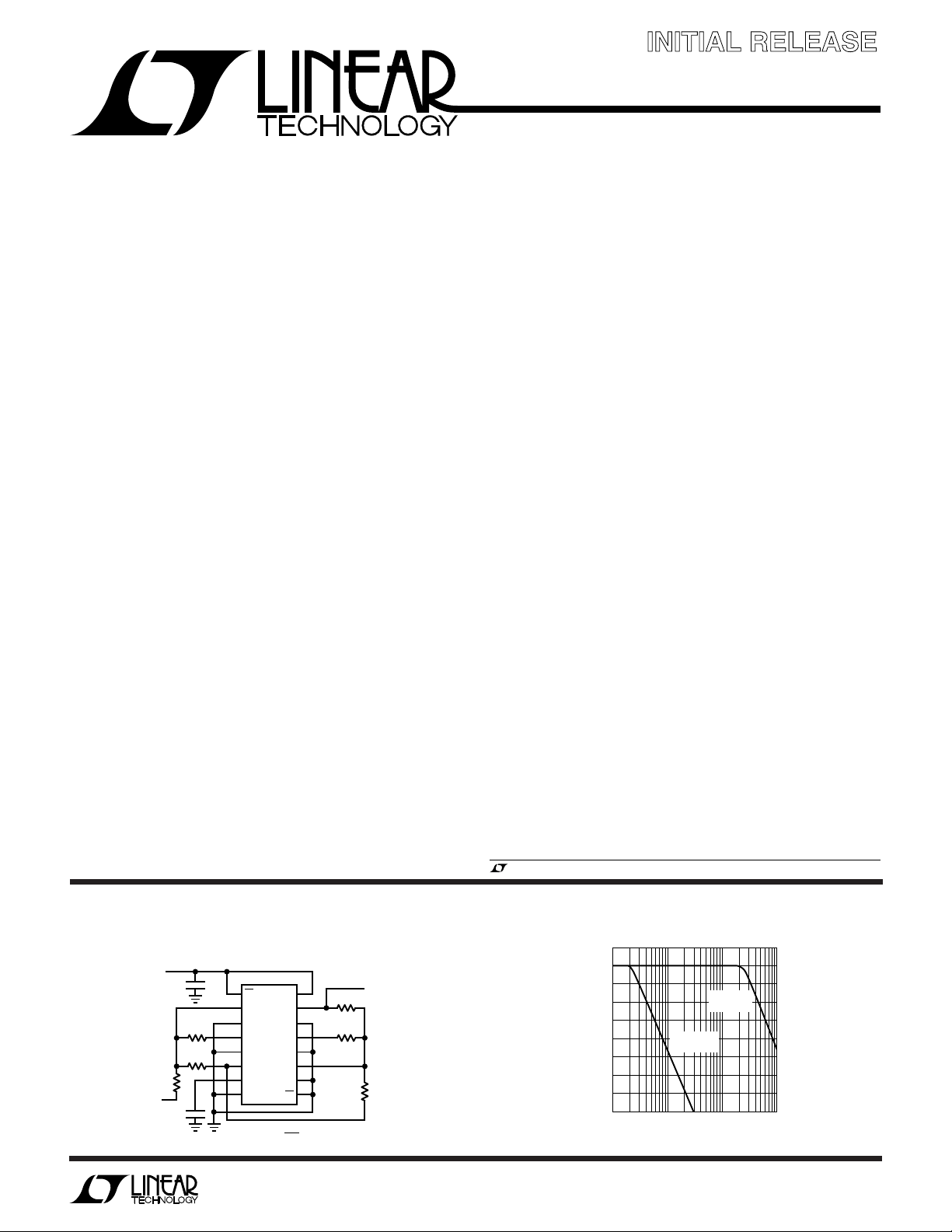
TYPICAL APPLICATION
Single 3.3V, 2.56kHz to 256kHz Butterworth Lowpass Filter
3.3V
V
0.1µF
R
R
R
IN
1µF
LTC1563-2
1
LP
2
SA
3
NC
4
INVA
5
NC
6
LPA
7
AGND
8
V
= 256kHz
f
C
–
16
+
V
15
LPB
14
NC
13
INVB
12
NC
11
SB
10
NC
9
EN
10k
()
R
Information furnished by Linear Technology Corporation is believed to be accurate and reliable.
However, no responsibility is assumed for its use. Linear Technology Corporation makes no representation that the interconnection of its circuits as described herein will not infringe on existing patent rights.
R
R
1563 TA01
V
OUT
R
, LTC and LT are registered trademarks of Linear Technology Corporation.
Frequency Response
10
0
–10
–20
–30
–40
GAIN (dB)
–50
–60
–70
–80
R = 1M
f
C
10k1k
FREQUENCY (Hz)
= 2.56kHz
R = 10k
= 256kHz
f
C
100k 1M
1563 TA02
1
Page 2
LTC1563-2/LTC1563-3
WW
W
ABSOLUTE MAXIMUM RA TIN GS
U
U
W
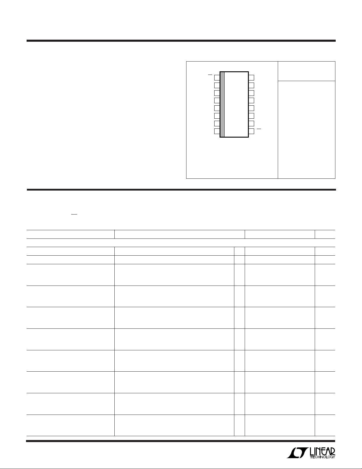
PACKAGE/ORDER INFORMATION
(Note 1)
Total Supply Voltage (V+ to V–)............................... 11V
Maximum Input Voltage at
Any Pin ....................... (V– – 0.3V) ≤ V
≤ (V+ + 0.3V)
PIN
Power Dissipation.............................................. 500mW
Operating Temperature Range
LTC1563C ...............................................0°C to 70°C
LTC1563I............................................ –40°C to 85°C
Storage Temperature Range................. –65°C to 150°C
Lead Temperature (Soldering, 10 sec)..................300°C
TOP VIEW
LP
1
2
SA
3
NC
4
INVA
5
NC
6
LPA
7
AGND
–
8
V
16-LEAD NARROW PLASTIC SSOP
NOTE: PINS LABELED NC ARE NOT CONNECTED
INTERNALLY AND SHOULD BE CONNECTED TO THE
SYSTEM GROUND
Consult factory for Military grade parts.
GN PACKAGE
T
= 150°C, θJA = 135°C/W
JMAX
+
16
V
15
LPB
14
NC
13
INVB
12
NC
11
SB
10
NC
9
EN
ORDER PART
NUMBER
LTC1563-2CGN
LTC1563-3CGN
LTC1563-2IGN
LTC1563-3IGN
ELECTRICAL CHARACTERISTICS
The ● denotes specifications which apply over the full operating temperature range, otherwise specifications are TA = 25°C.
VS = Single 4.75V, EN pin to logic “low,” Gain = 1, R
speed (HS) and low power (LP) modes unless otherwise noted.
= R11 = R21 = R31 = R12 = R22 = R32, specifications apply to both the high
FIL
U
PARAMETER CONDITIONS MIN TYP MAX UNITS
Specifications for Both LTC1563-2 and LTC1563-3
Total Supply Voltage (VS), HS Mode ● 311V
Total Supply Voltage (VS), LP Mode ● 2.7 11 V
Positive Output Voltage Swing (LPB Pin) VS = 3V, fC = 25.6kHz, R
HS Mode V
Negative Output Voltage Swing (LPB Pin) VS = 3V, fC = 25.6kHz, R
HS Mode V
Positive Output Swing (LPB Pin) VS = 2.7V, fC = 25.6kHz, R
LP Mode V
Negative Output Swing (LPB Pin) VS = 2.7V, fC = 25.6kHz, R
LP Mode V
DC Offset Voltage, HS Mode VS = 3V, fC = 25.6kHz, R
(Section A Only) V
DC Offset Voltage, LP Mode V
(Section A Only) V
DC Offset Voltage, HS Mode V
(Input to Output, Sections A, B Cascaded) V
DC Offset Voltage, LP Mode V
(Input to Output, Sections A, B Cascaded) V
= 4.75V, fC = 25.6kHz, R
S
VS = ±5V, fC = 25.6kHz, R
= 4.75V, fC = 25.6kHz, R
S
VS = ±5V, fC = 25.6kHz, R
= 4.75V, fC = 25.6kHz, R
S
VS = ±5V, fC = 25.6kHz, R
= 4.75V, fC = 25.6kHz, R
S
VS = ±5V, fC = 25.6kHz, R
= 4.75V, fC = 25.6kHz, R
S
VS = ±5V, fC = 25.6kHz, R
= 2.7V, fC = 25.6kHz, R
S
= 4.75V, fC = 25.6kHz, R
S
VS = ±5V, fC = 25.6kHz, R
= 3V, fC = 25.6kHz, R
S
= 4.75V, fC = 25.6kHz, R
S
VS = ±5V, fC = 25.6kHz, R
= 2.7V, fC = 25.6kHz, R
S
= 4.75V, fC = 25.6kHz, R
S
VS = ±5V, fC = 25.6kHz, R
= 100k, RL = 10k to GND ● 2.9 2.95 V
FIL
= 100k, RL = 10k to GND ● 4.55 4.7 V
FIL
= 100k, RL = 10k to GND ● 4.8 4.9 V
FIL
= 100k, RL = 10k to GND ● 0.015 0.05 V
FIL
= 100k, RL = 10k to GND ● 0.02 0.05 V
FIL
= 100k, RL = 10k to GND ● –4.95 –4.9 V
FIL
= 100k, RL = 10k to GND ● 2.6 2.65 V
FIL
= 100k, RL = 10k to GND ● 4.55 4.65 V
FIL
= 100k, RL = 10k to GND ● 4.8 4.9 V
FIL
= 100k, RL = 10k to GND ● 0.01 0.05 V
FIL
= 100k, RL = 10k to GND ● 0.015 0.05 V
FIL
= 100k, RL = 10k to GND ● –4.95 –4.9 V
FIL
= 100k ● ±1.5 ±3mV
FIL
= 100k ● ±1.0 ±3mV
FIL
= 100k ● ±1.5 ±3mV
FIL
= 100k ● ±2 ±4mV
FIL
= 100k ● ±2 ±4mV
FIL
= 100k ● ±2 ±5mV
FIL
= 100k ● ±1.5 ±3mV
FIL
= 100k ● ±1.0 ±3mV
FIL
= 100k ● ±1.5 ±3mV
FIL
= 100k ● ±2 ±5mV
FIL
= 100k ● ±2 ±5mV
FIL
= 100k ● ±2 ±6mV
FIL
2
Page 3
LTC1563-2/LTC1563-3
ELECTRICAL CHARACTERISTICS
The ● denotes specifications which apply over the full operating temperature range, otherwise specifications are TA = 25°C.
VS = Single 4.75V, EN pin to logic “low,” Gain = 1, R
speed (HS) and low power (LP) modes unless otherwise noted.
PARAMETER CONDITIONS MIN TYP MAX UNITS
DC Offset Voltage Drift, HS Mode VS = 3V, fC = 25.6kHz, R
(Input to Output, Sections A, B) V
DC Offset Voltage Drift, LP Mode V
(Input to Output, Sections A, B) V
AGND Voltage VS = 4.75V, fC = 25.6kHz, R
Power Supply Current, HS Mode VS = 3V, fC = 25.6kHz, R
Power Supply Current, LP Mode VS = 2.7V, fC = 25.6kHz, R
Shutdown Mode Supply Current VS = 4.75V, fC = 25.6kHz, R
EN Input V
Logic Low Level V
EN Input V
Logic High Level V
LP VS = 3V ● 0.8 V
Logic Low Level V
LP VS = 3V ● 2.5 V
Logic High Level V
LTC1563-2 Transfer Function Characteristics
Cutoff Frequency Range, f
C
HS Mode V
Cutoff Frequency Range, f
C
LP Mode V
Cutoff Frequency Accuracy, HS Mode V
= 25.6kHz VS = 4.75V, R
f
C
Cutoff Frequency Accuracy, HS Mode V
= 256kHz VS = 4.75V, R
f
C
Cutoff Frequency Accuracy, LP Mode VS = 2.7V, R
= 25.6kHz VS = 4.75V, R
f
C
Cutoff Frequency Temperature Coefficient ● ±1 ppm/°C
Passband Gain, HS Mode, fC = 25.6kHz Test Frequency = 2.56kHz (0.1 • fC) ● –0.2 0 0.2 dB
VS = 4.75V, R
= 100k Test Frequency = 12.8kHz (0.5 • fC) ● –0.3 0 0.3 dB
FIL
= 4.75V, fC = 25.6kHz, R
S
VS = ±5V, fC = 25.6kHz, R
= 2.7V, fC = 25.6kHz, R
S
= 4.75V, fC = 25.6kHz, R
S
VS = ±5V, fC = 25.6kHz, R
V
= 4.75V, fC = 25.6kHz, R
S
VS = ±5V, fC = 25.6kHz, R
V
= 4.75V, fC = 25.6kHz, R
S
VS = ±5V, fC = 25.6kHz, R
= 3V ● 0.8 V
S
= 4.75V ● 1V
S
VS = ±5V ● 1V
= 3V ● 2.5 V
S
= 4.75V ● 4.3 V
S
VS = ±5V ● 4.4 V
= 4.75V ● 1V
S
VS = ±5V ● 1V
= 4.75V ● 4.3 V
S
VS = ±5V ● 4.4 V
VS = 3V ● 5 256 kHz
= 4.75V ● 5 256 kHz
S
VS = ±5V ● 5 256 kHz
VS = 2.7V ● 5 25.6 kHz
= 4.75V ● 5 25.6 kHz
S
VS = ±5V ● 5 25.6 kHz
= 3V, R
S
VS = ±5V, R
= 3V, R
S
VS = ±5V, R
VS = ±5V, R
= R11 = R21 = R31 = R12 = R22 = R32, specifications apply to both the high
FIL
= 100k ● 5 µV/°C
FIL
= 100k ● 5 µV/°C
FIL
= 100k ● 5 µV/°C
FIL
= 100k ● 5 µV/°C
FIL
= 100k ● 5 µV/°C
FIL
= 100k ● 5 µV/°C
FIL
= 100k ● 2.35 2.375 2.40 V
FIL
= 100k ● 8.0 14 mA
FIL
= 100k ● 10.5 17 mA
FIL
= 100k ● 15 23 mA
FIL
= 100k ● 1.0 1.8 mA
FIL
= 100k ● 1.4 2.5 mA
FIL
= 100k ● 2.3 3.5 mA
FIL
= 100k ● 120 µA
FIL
= 100k ● –1.5 ±1.5 3.5 %
FIL
= 100k ● –1.5 ±1.5 3.5 %
FIL
= 100k ● –1.5 ±1.5 3.5 %
FIL
= 10k ● –5 ±1.5 1.5 %
FIL
= 10k ● –5 ±1.5 1.5 %
FIL
= 10k ● –5 ±1.5 1.5 %
FIL
= 100k ● –3 ±1.5 3 %
FIL
= 100k ● –3 ±1.5 3 %
FIL
= 100k ● –3 ±1.5 3 %
FIL
3
Page 4
LTC1563-2/LTC1563-3
ELECTRICAL CHARACTERISTICS
The ● denotes specifications which apply over the full operating temperature range, otherwise specifications are TA = 25°C.
VS = Single 4.75V, EN pin to logic “low,” Gain = 1, R
speed (HS) and low power (LP) modes unless otherwise noted.
PARAMETER CONDITIONS MIN TYP MAX UNITS
Stopband Gain, HS Mode, f
VS = 4.75V, R
= 100k Test Frequency = 102.4kHz (4 • fC) ● –48 –46 dB
FIL
Passband Gain, HS Mode, fC = 256kHz Test Frequency = 25.6kHz (0.1 • fC) ● –0.2 0 0.2 dB
VS = 4.75V, R
= 10k Test Frequency = 128kHz (0.5 • fC) ● –0.5 0 0.5 dB
FIL
Stopband Gain, HS Mode, f
VS = 4.75V, R
= 10k Test Frequency = 500kHz (1.95 • fC) ● –23.3 –21.5 dB
FIL
Passband Gain, LP Mode, f
VS = 4.75V, R
= 100k Test Frequency = 12.8kHz (0.5 • fC) ● –0.6 –0.02 0.6 dB
FIL
Stopband Gain, LP Mode, f
VS = 4.75V, R
= 100k Test Frequency = 102.4kHz (4 • fC) ● –48 –46.5 dB
FIL
LTC1563-3 Transfer Function Characteristics
Cutoff Frequency Range, f
HS Mode VS = 4.75V ● 5 256 kHz
Cutoff Frequency Range, f
LP Mode V
Cutoff Frequency Accuracy, HS Mode V
= 25.6kHz VS = 4.75V, R
f
C
Cutoff Frequency Accuracy, HS Mode V
= 256kHz VS = 4.75V, R
f
C
Cutoff Frequency Accuracy, LP Mode V
= 25.6kHz VS = 4.75V, R
f
C
Cutoff Frequency Temperature Coefficient ● ±1 ppm/°C
Passband Gain, HS Mode, fC = 25.6kHz Test Frequency = 2.56kHz (0.1 • fC) ● –0.2 –0.03 0.2 dB
VS = 4.75V, R
= 100k Test Frequency = 12.8kHz (0.5 • fC) ● –1.0 –0.72 –0.25 dB
FIL
Stopband Gain, HS Mode, f
VS = 4.75V, R
= 100k Test Frequency = 102.4kHz (4 • fC) ● –34.7 –31 dB
FIL
Passband Gain, HS Mode, f
VS = 4.75V, R
= 10k Test Frequency = 128kHz (0.5 • fC) ● –1.1 –0.72 –0.5 dB
FIL
Stopband Gain, HS Mode, f
VS = 4.75V, R
= 10k Test Frequency = 500kHz (1.95 • fC) ● –13 –10.5 dB
FIL
Passband Gain, LP Mode, f
VS = 4.75V, R
= 100k Test Frequency = 12.8kHz (0.5 • fC) ● –1.0 –0.72 –0.25 dB
FIL
Stopband Gain, LP Mode, f
VS = 4.75V, R
= 100k Test Frequency = 102.4Hz (4 • fC) ● –34.7 –32 dB
FIL
Note 1: Absolute Maximum Ratings are those value beyond which the life
of a device may be impaired.
= 25.6kHz Test Frequency = 51.2kHz (2 • fC) ● –24 –21.5 d B
C
= 256kHz Test Frequency = 400kHz (1.56 • fC) ● –15.7 –13.5 dB
C
= 25.6kHz Test Frequency = 2.56kHz (0.1 • fC) ● –0.25 0 0.25 dB
C
= 25.6kHz Test Frequency = 51.2kHz (2 • fC) ● –24 –22 dB
C
C
VS = 3V ● 5 256 kHz
VS = ±5V ● 5 256 kHz
C
VS = 2.7V ● 5 25.6 kHz
= 4.75V ● 5 25.6 kHz
S
VS = ±5V ● 5 25.6 kHz
= 3V, R
S
VS = ±5V, R
= 3V, R
S
VS = ±5V, R
= 2.7V, R
S
VS = ±5V, R
= 25.6kHz Test Frequency = 51.2kHz (2 • fC) ● –13.6 –10 dB
C
= 256kHz Test Frequency = 25.6kHz (0.1 • fC) ● –0.2 –0.03 0.2 dB
C
= 256kHz Test Frequency = 400kHz (1.56 • fC) ● –8.3 –6 dB
C
= 25.6kHz Test Frequency = 2.56kHz (0.1 • fC) ● –0.2 –0.03 0.2 dB
C
= 25.6kHz Test Frequency = 51.2kHz (2 • fC) ● –13.6 –11 dB
C
= R11 = R21 = R31 = R12 = R22 = R32, specifications apply to both the high
FIL
= 100k ● –2 ±2 5.5 %
FIL
= 100k ● –2 ±2 5.5 %
FIL
= 100k ● –2 ±2 5.5 %
FIL
= 10k ● –2 ±26 %
FIL
= 10 ● –2 ±26 %
FIL
= 10k ● –2 ±26 %
FIL
= 100k ● –3 ±37 %
FIL
= 100k ● –3 ±37 %
FIL
= 100k ● –3 ±37 %
FIL
4
Page 5

UUU
PIN FUNCTIONS
LTC1563-2/LTC1563-3
LP (Pin 1): Low Power. The LTC1563-X has two operating
modes. Most applications use the part’s High Speed
operating mode. Some lower frequency, lower gain applications can take advantage of the Low Power mode. When
placed in the Low Power mode, the supply current is nearly
an order of magnitude lower than the High Speed mode.
Refer to the Applications Information section for more
information on the Low Power mode.
The LTC1563-X is in the High Speed mode when the
LP input is at a logic high level or is open-circuited. A small
pull-up current source at the LP input defaults the
LTC1563-X to the High Speed mode if the pin is left open.
The part is in the Low Power mode when the pin is pulled
to a logic low level or connected to V–.
SA, SB (Pins 2, 11): Summing Pins. These pins are a
summing point for signals fed forward and backward.
Capacitance on the SA or SB pin will cause excess peaking
of the frequency response near the cutoff frequency. The
three external resistors for each section should be located
as close as possible to the summing pin to minimize this
effect. Refer to the Applications Information section for
more details.
NC (Pins 3, 5, 10, 12, 14): These pins are not connected
internally. For best performance, they should be connected to ground.
INVA, INVB (Pins 4, 13): Inverting Input. Each of the INV
pins is an inverting input of an op amp. Note that the INV
pins are high impedance, sensitive nodes of the filter and
very susceptible to coupling of unintended signals.
Capacitance on the INV nodes will also affect the frequency response of the filter sections. For these reasons,
printed circuit connections to the INV pins must be kept as
short as possible.
LPA, LPB (Pins 6, 15): Lowpass Output. These pins are
the rail-to-rail outputs of an op amp. Each output is
designed to drive a nominal net load of 5kΩ and 20pF.
Refer to the Applications Information section for more
details on output loading effects.
AGND (Pin 7): Analog Ground. The AGND pin is the
midpoint of an internal resistive voltage divider developing
a potential halfway between the V+ and V– pins. The
equivalent series resistance is nominally 10kΩ. This serves
as an internal ground reference. Filter performance will
reflect the quality of the analog signal ground. An analog
ground plane surrounding the package is recommended.
The analog ground plane should be connected to any
digital ground at a single point. Figures 1 and 2 show the
proper connections for dual and single supply operation.
V–, V+ (Pins 8, 16): The V– and V+ pins should be
bypassed with 0.1µF capacitors to an adequate analog
ground or ground plane. These capacitors should be
connected as closely as possible to the supply pins. Low
noise linear supplies are recommended. Switching supplies are not recommended as they will decrease the
filter’s dynamic range. Refer to Figures 1 and 2 for the
proper connections for dual and single supply operation.
EN (Pin 9): ENABLE. When the EN input goes high or is
open-circuited, the LTC1563-X enters a shutdown state
and only junction leakage currents flow. The AGND pin, the
LPA output and the LPB output assume high impedance
states. If an input signal is applied to a complete filter
circuit while the LTC1563-X is in shutdown, some signal
will normally flow to the output through passive components around the inactive part.
A small internal pull-up current source at the EN input
defaults the LTC1563 to the shutdown state if the EN pin
is left floating
to V– (or a logic low) to enable the part for normal
operation.
. Therefore, the user
must
connect the EN pin
5
Page 6

LTC1563-2/LTC1563-3
UUU
PIN FUNCTIONS
ANALOG
GROUND
PLANE
–
V
0.1µF
SINGLE POINT
SYSTEM GROUND
1
LP
2
SA
3
NC
4
INVA
5
NC
6
LPA
7
AGND
8
V
LTC1563-X
–
LPB
INVB
V
NC
NC
SB
NC
EN
+
16
15
14
13
12
11
10
9
DIGITAL
GROUND PLANE
(IF ANY)
V
0.1µF
+
1563 F01
ANALOG
GROUND
PLANE
+
1µF
SINGLE POINT
SYSTEM GROUND
1
2
3
4
5
6
7
8
LTC1563-X
LP
SA
NC
INVA
NC
LPA
AGND
–
V
LPB
NC
INVB
NC
SB
NC
EN
+
V
16
15
14
13
12
11
10
9
DIGITAL
GROUND PLANE
(IF ANY)
Figure 1. Dual Supply Power and Ground Connections Figure 2. Single Supply Power and Ground Connections
W
BLOCK DIAGRA
V
0.1µF
+
1563 F02
SHUTDOWN
SWITCH
AGND
7
SHUTDOWN
SWITCH
PATENT PENDING
+
V
16
20k
20k
–
8 1
V
9
V
IN
AGND
EN
LP
R11
R21
R31
C1A
SA
2
4
INVA
C2A
AGND
–
+
R12
LPA
6
LTC1563-X
R32
11
SB
C2B
13
INVB
AGND
R22
V
OUT
C1B
–
15
+
LPB
1563 BD
6
Page 7

LTC1563-2/LTC1563-3
U
WUU
APPLICATIONS INFORMATION
Functional Description
The LTC1563-2/LTC1563-3 are a family of easy-to-use,
4th order lowpass filters with rail-to-rail operation. The
LTC1563-2, with a single resistor value, gives a unity-gain
filter approximating a Butterworth response. The
LTC1563-3, with a single resistor value, gives a unity-gain
filter approximating a Bessel (linear phase) response. The
proprietary architecture of these parts allows for a simple
unity-gain resistor calculation:
R = 10k(256kHz/fC)
where fC is the desired cutoff frequency. For many applications, this formula is all that is needed to design a filter.
For example, a 50kHz filter requires a 51.2k resistor. In
practice, a 51.1k resistor would be used as this is the
closest E96, 1% value available.
The LTC1563-X is constructed with two 2nd order sections. The output of the first section (section A) is simply
fed into the second section (section B). Note that section
A and section B are similar, but not identical. The parts are
designed to be simple and easy to use.
By simply utilizing different valued resistors, gain and
other transfer functions are achieved. For these applications, the resistor value calculation gets more difficult. The
tables of formulas provided later in this section make this
task much easier. For best results, design these filters
using FilterCADTM Version 3.0 (or newer) or contact the
Linear Technology Filter Applications group for assistance.
in parallel, yields a net effective resistance of 952k and an
error of –5%. Note that the gain is also limited to unity at
the minimum fC.
At intermediate fC, the gain is limited by one of the two
reasons discussed above. For best results, design filters
with gain using FilterCAD Version 3 (or newer) or contact
the Linear Technology Filter Applications Group for assistance.
DC Offset, Noise and Gain Considerations
The LTC1563-X is DC offset trimmed in a 2-step manner.
First, section A is trimmed for minimum DC offset. Next,
section B is trimmed to minimize the total DC offset
(section A
minimum DC offset in unity gain applications and most
higher gain applications.
For gains greater than unity, the gain should be distributed
such that most of the gain is taken in section A, with
section B at a lower gain (preferably unity). This type of
gain distribution results in the lowest noise and lowest DC
offset. For high gain, low frequency applications, all of the
gain is taken in section A, with section B set for unity-gain.
In this configuration, the noise and DC offset is dominated
by those of section A. At higher frequencies, the op amps’
finite bandwidth limits the amount of gain that section A
can reliably achieve. The gain is more evenly distributed in
this case. The noise and DC offset of section A is now
multiplied by the gain of section B. The result is slightly
higher noise and offset.
plus
section B). This method is used to give the
Cutoff Frequency (fC) and Gain limitations
The LTC563-X has both a maximum fC limit and a minimum fC limit. The maximum fC limit (256kHz in High Speed
mode and 25.6kHz in the Low Power mode) is set by the
speed of the LTC1563-X’s op amps. At the maximum fC,
the gain is also limited to unity.
A minimum fC is dictated by the practical limitation of
reliably obtaining large valued, precision resistors. As the
desired fC decreases, the resistor value required increases.
When fC is 2.56kHz, the resistors are 1M. Obtaining a
reliable, precise 1M resistance between two points on a
printed circuit board is somewhat difficult. For example, a
1M resistor with 20MΩ of stray, layout related resistance
Output Loading: Resistive and Capacitive
The op amps of the LTC1563-X have a rail-to-rail output
stage. To obtain maximum performance, the output loading effects must be considered. Output loading issues can
be divided into resistive effects and capacitive effects.
Resistive loading affects the maximum output signal swing
and signal distortion. If the output load is excessive, the
output swing is reduced and distortion is increased. All of
the output voltage swing testing on the LTC1563-X is done
with R22 = 100k and a 10k load resistor. For best undistorted
output swing, the output load resistance should be greater
than 10k.
FilterCAD is trademark of Linear Technology Corporation.
7
Page 8

LTC1563-2/LTC1563-3
U
WUU
APPLICATIONS INFORMATION
Capacitive loading on the output reduces the stability of
the op amp. If the capacitive loading is sufficiently high,
the stability margin is decreased to the point of oscillation
at the output. Capacitive loading should be kept below
30pF. Good, tight layout techniques should be maintained
at all times. These parts should not drive long traces and
must never drive a long coaxial cable.
LTC1563-X, always use a 10x probe. Never use a 1x probe
A standard 10x probe has a capacitance of 10pF to 15pF
while a 1x probe’s capacitance can be as high as 150pF.
The use of a 1x probe will probably cause oscillation.
For larger capacitive loads, a series isolation resistor can
be used between the part and the capacitive load. If the
load is too great, a buffer must be used.
Layout Precautions
The LTC1563-X is an active RC filter. The response of the
filter is determined by the on-chip capacitors and the
external resistors. Any external, stray capacitance in parallel with an on-chip capacitor, or to an AC ground, can
alter the transfer function.
When probing the
.
Capacitance to an AC ground is the most likely problem.
Capacitance on the LPA or LPB pins does not affect the
transfer function but does affect the stability of the op
amps. Capacitance on the INVA and INVB pins will affect
the transfer function somewhat and will also affect the
stability of the op amps. Capacitance on the SA and SB
pins alters the transfer function of the filter. These pins are
the most sensitive to stray capacitance. Stray capacitance
on these pins results in peaking of the frequency response
near the cutoff frequency. Poor layout can give 0.5dB to
1dB of excess peaking.
To minimize the effects of parasitic layout capacitance, all
of the resistors for section A should be placed as close as
possible to the SA pin. Place the R31 resistor first so that
it is as close as possible to the SA pin on one end and as
close as possible to the INVA pin on the other end. Use the
same strategy for the layout of section B, keeping all of the
resistors as close as possible to the SB node and first
placing R32 between the SB and INVB pins. It is also best
if the signal routing and resistors are on the same layer as
the part without any vias in the signal path.
8
Page 9

U
TYPICAL APPLICATIO S
4th Order Filter Responses Using the LTC1563-2
LTC1563-2
1
LP
2
SA
3
R31
R21
R11
V
IN
NC
4
INVA
5
NC
6
LPA
7
AGND
8
–
V
Figure 3. 4th Order Filter Connections (Power Supply, Ground,
EN and LP Connections Not Shown for Clarity). Table 1 Shows
Resistor Values
LPB
INVB
V
NC
NC
SB
NC
EN
16
+
15
14
13
12
11
10
R22
R32
9
R12
1563 F03
V
OUT
LTC1563-2/LTC1563-3
10
0
–20
–40
GAIN (dB)
–60
–80
–90
BUTTERWORTH
0.5dB RIPPLE
CHEBYSHEV
0.1dB RIPPLE
CHEBYSHEV
NORMALIZED TO fC = 1Hz
0.1
FREQUENCY (Hz)
Figure 3a. Frequency Response
101
1563 F03a
1
0
–2
–4
GAIN (dB)
–6
–8
–10
BUTTERWORTH
0.5dB RIPPLE
CHEBYSHEV
0.1dB RIPPLE
CHEBYSHEV
NORMALIZED TO fC = 1Hz
0.1
FREQUENCY (Hz)
21
1563 F03b
Figure 3b. Passband Frequency Response
1.2
1.0
0.8
0.6
0.4
OUTPUT VOLTAGE (V)
0.2
0
0
Figure 3c. Step Response
1.00.5 1.5 2.0
Table 1. Resistor Values, Normalized to 256kHz Cutoff Frequency (fC), Figure 3. The Passband
Gain, of the 4th Order LTC1563-2 Lowpass Filter, Is Set to Unity. (Note 1)
0.1dB RIPPLE 0.5dB RIPPLE
BUTTERWORTH CHEBYSHEV CHEBYSHEV
LP Mode Max f
HS Mode Max f
C
C
R11 = R21 = 10k(256kHz/fC) 13.7k(256kHz/fC) 20.5k(256kHz/fC)
R31 = 10k(256kHz/fC) 10.7k(256kHz/fC) 12.4k(256kHz/fC)
R12 = R22 = 10k(256kHz/fC) 10k(256kHz/fC) 12.1k(256kHz/fC)
R32 = 10k(256kHz/fC) 6.81k(256kHz/fC) 6.98k(256kHz/fC)
25.6kHz 15kHz 13kHz
256kHz 135kHz 113kHz
BUTTERWORTH
0.5dB RIPPLE
CHEBYSHEV
0.1dB RIPPLE
CHEBYSHEV
NORMALIZED TO fC = 1Hz
2.5 3.0
TIME (s)
1563 F03C
Example: In HS mode, 0.1dB ripple Chebyshev, 100kHz cutoff frequency, R11 = R21 = 35k ≅ 34.8k (1%),
R31 = 27.39k ≅ 27.4k (1%), R12 = R22 = 256k ≅ 255k (1%), R32 = 17.43k ≅ 17.4k (1%)
Note 1: The resistor values listed in this table provide good approximations of the listed transfer functions. For the
optimal resistor values, higher gain or other transfer functions, use FilterCAD Version 3.0 (or newer) or contact the
Linear Technology Filter Applications group for assistance.
9
Page 10

LTC1563-2/LTC1563-3
U
TYPICAL APPLICATIO S
4th Order Filter Responses Using the LTC1563-3
LTC1563-3
1
LP
2
SA
3
R31
R21
R11
V
IN
NC
4
INVA
5
NC
6
LPA
7
AGND
8
–
V
Figure 4. 4th Order Filter Connections (Power Supply, Ground,
EN and LP Connections Not Shown for Clarity). Table 2 Shows
Resistor Values
LPB
NC
INVB
NC
NC
16
+
V
SB
EN
R22
15
14
R32
13
12
11
10
9
R12
1563 F04
V
OUT
10
0
–20
–40
GAIN (dB)
–60
–80
–90
BESSEL
TRANSITIONAL
GAUSSIAN TO 12dB
TRANSITIONAL
GAUSSIAN TO 6dB
NORMALIZED TO fC = 1Hz
0.1
FREQUENCY (Hz)
Figure 4a. Frequency Response
101
1563 F04a
1.2
1.0
0.8
0.6
0.4
OUTPUT VOLTAGE (V)
0.2
0
0
BESSEL
TRANSITIONAL
GAUSSIAN TO 12dB
TRANSITIONAL
GAUSSIAN TO 6dB
NORMALIZED TO fC = 1Hz
1.00.5 1.5 2.0
TIME (s)
2.5 3.0
1563 F04b
1.05
1.00
OUTPUT VOLTAGE (V)
0.95
BESSEL
TRANSITIONAL
GAUSSIAN TO 12dB
TRANSITIONAL
GAUSSIAN TO 6dB
0
0.5
NORMALIZED TO fC = 1Hz
1.0
TIME (s)
Figure 4b. Step Response Figure 4c. Step Response—Settling
Table 2. Resistor Values, Normalized to 256kHz Cutoff Frequency (fC), Figure 4. The Passband
Gain, of the 4th Order LTC1563-3 Lowpass Filter, Is Set to Unity. (Note 1)
TRANSITIONAL TRANSITIONAL
BESSEL GAUSSIAN TO 6dB GAUSSIAN TO 12dB
LP Mode Max f
HS Mode Max f
C
C
R11 = R21 = 10k(256kHz/fC) 17.4k(256kHz/fC) 15k(256kHz/fC)
R31 = 10k(256kHz/fC) 13.3k(256kHz/fC) 11.8k(256kHz/fC)
R12 = R22 = 10k(256kHz/fC) 14.3k(256kHz/fC) 10.5k(256kHz/fC)
R32 = 10k(256kHz/fC) 6.04k(256kHz/fC) 6.19k(256kHz/fC)
Note 1: The resistor values listed in this table provide good approximations of the listed transfer functions. For the
optimal resistor values, higher gain or other transfer functions, use FilterCAD Version 3.0 (or newer) or contact the
Linear Technology Filter Applications group for assistance.
25.6kHz 20kHz 21kHz
256kHz 175kHz 185kHz
1.5
2.0
1563 F04c
10
Page 11

U
TYPICAL APPLICATIO S
LTC1563-2/LTC1563-3
±5V, 2.3mA Supply Current, 20kHz, 4th Order,
0.5dB Ripple Chebyshev Lowpass Filter
LTC1563-2
1
LP
2
SA
3
162k
V
IN
267k267k
–5V
0.1µF
NC
4
INVA
5
NC
6
LPA
7
AGND
8
–
V
LPB
NC
INVB
NC
SB
NC
EN
16
+
V
15
14
13
12
11
10
9
Single 3.3V, 2mA Supply Current, 20kHz 8th Order Butterworth Lowpass Filter
LTC1563-2 LTC1563-2
1
LP
2
SA
3
113k
133k
113k
1µF
V
IN
NC
4
INVA
5
NC
6
LPA
7
AGND
8
–
V
LPB
NC
INVB
NC
SB
NC
EN
158k
93.1k
+
V
Frequency Response
10
V
OUT
5V
0.1µF
158k
ENABLE
1563 TA03
0.1µF 0.1µF
16
80.6k
15
14
191k
13
12
11
10
9
205k
73.2k
205k
80.6k
1µF
0
–10
–20
–30
–40
GAIN (dB)
–50
–60
–70
–80
–90
1
1
LP
2
SA
3
NC
4
INVA
5
NC
6
LPA
7
AGND
8
–
V
FREQUENCY (kHz)
16
+
V
15
LPB
14
NC
13
INVB
12
NC
11
SB
10
NC
9
EN
10 100
1563 TA04
3.3V
V
154k
97.6k
OUT
154k
1563 TA05
ENABLE
10
0
–10
–20
–30
–40
GAIN (dB)
–50
–60
–70
–80
–90
1
Frequency Response
10 100
FREQUENCY (kHz)
1563 TA06
11
Page 12

LTC1563-2/LTC1563-3
U
TYPICAL APPLICATIO S
Single 3.3V, 256kHz Bessel Lowpass Filter Frequency Response
LTC1563-3
1
LP
2
SA
3
10k
10k
10k
V
IN
1µF
NC
4
INVA
5
NC
6
LPA
7
AGND
8
–
V
LPB
NC
INVB
NC
NC
16
+
V
SB
EN
10k
15
14
10k
13
12
11
10
9
PACKAGE DESCRIPTION
0.015
± 0.004
× 45°
0.007 – 0.0098
(0.178 – 0.249)
(0.38 ± 0.10)
0° – 8° TYP
3.3V
0.1µF
V
OUT
10k
ENABLE
1563 TA07
U
GN Package
16-Lead Plastic SSOP (Narrow 0.150)
(LTC DWG # 05-08-1641)
0.053 – 0.068
(1.351 – 1.727)
0.004 – 0.0098
(0.102 – 0.249)
10
0
–10
–20
GAIN (dB)
–30
–40
–50
10k
100k 1M
FREQUENCY (Hz)
0.189 – 0.196*
(4.801 – 4.978)
16
15
14
12 11 10
13
1563 TA08
9
0.009
(0.229)
REF
0.016 – 0.050
(0.406 – 1.270)
* DIMENSION DOES NOT INCLUDE MOLD FLASH. MOLD FLASH
SHALL NOT EXCEED 0.006" (0.152mm) PER SIDE
** DIMENSION DOES NOT INCLUDE INTERLEAD FLASH. INTERLEAD
FLASH SHALL NOT EXCEED 0.010" (0.254mm) PER SIDE
0.008 – 0.012
(0.203 – 0.305)
0.0250
(0.635)
BSC
0.229 – 0.244
(5.817 – 6.198)
12
5
4
3
678
RELATED PARTS
PART NUMBER DESCRIPTION COMMENTS
LTC1560-1 5-Pole Elliptic Lowpass, fC = 1MHz/0.5MHz No External Components, SO-8
LTC1562 Universal Quad 2-Pole Active RC 10kHz < fO < 150kHz
LTC1562-2 Universal Quad 2-Pole Active RC 20kHz < fO < 300kHz
LTC1569-6 Low Power 10-Pole Delay Equalized Elliptic Lowpass fC < 80kHz, One Resistor Sets fC, SO-8
LTC1569-7 10-Pole Delay Equalized Elliptic Lowpass fC < 256kHz, One Resistor Sets fC, SO-8
156323i LT/TP 0100 4K • PRINTED IN USA
LINEAR TECHN OLOGY CORPORATION 2000
12
Linear Technology Corporation
1630 McCarthy Blvd., Milpitas, CA 95035-7417
(408) 432-1900 ● FAX: (408) 434-0507
●
www.linear-tech.com
0.150 – 0.157**
(3.810 – 3.988)
GN16 (SSOP) 1098
 Loading...