

Page 1
1
LTC1559-3.3/LTC1559-5
Backup Battery Controller
with Fixed Output
■
Complete Battery Backup System in an SO-8,
16-Pin GN or SO Package
■
Generates Fixed Backup Voltage (3.07V/4.63V) from
a Single 1.2V NiCd Button Cell
■
Automatic Main Supply to Backup Switching
■
Minimum 100mW Output Power
■
Automatic Fast Recharge of NiCd Battery
■
Programmable NiCd Trickle Charge Current
■
Smart NiCd Charger Minimizes Recharge Time and
Maximizes System Efficiency After Backup
■
Onboard Power-Up and Push-Button Reset
Generator
■
Performs VCC Supervisory Functions
■
Reset Assertion Guaranteed at VCC = 1V
■
Short-Circuit Protection
■
Thermal Limiting
FEATURES
DESCRIPTION
U
The LTC®1559 is a backup battery controller that provides
all the functions necessary to implement a backup 3.3V or
5V power supply using a single NiCd cell. It includes a 1.2V
to 3.07V/4.63V boost converter, an intelligent 2-stage
battery charger, automatic backup switching and a microprocessor reset generator. The boost converter uses a
synchronous switching architecture to achieve a typical
efficiency of 70%, ensuring maximum backup lifetime
from a small NiCd cell.
The on-chip NiCd charger uses an internal gas gauge to
minimize fast recharge time and prevent overcharging of
the backup cell, thereby improving system efficiency and
extending the life of the backup cell. The LTC1559 also
provides a user programmable trickle charge current to
compensate for self-discharge losses in the backup cell.
The LTC1559’s automatic backup switching scheme
requires minimum intervention from the host system and
provides feedback to the host to minimize system loading
in the backup state. Its internal VCC fault detector and reset
generator eliminate the need for a separate microprocessor supervisory chip in most applications.
The LTC1559 is available in an SO-8, 16-pin GN or SO
package.
APPLICATIONS
U
■
Notebook Computers
■
Palmtop Computers/PDAs
■
Portable Instruments
■
Battery-Powered Systems
, LTC and LT are registered trademarks of Linear Technology Corporation.
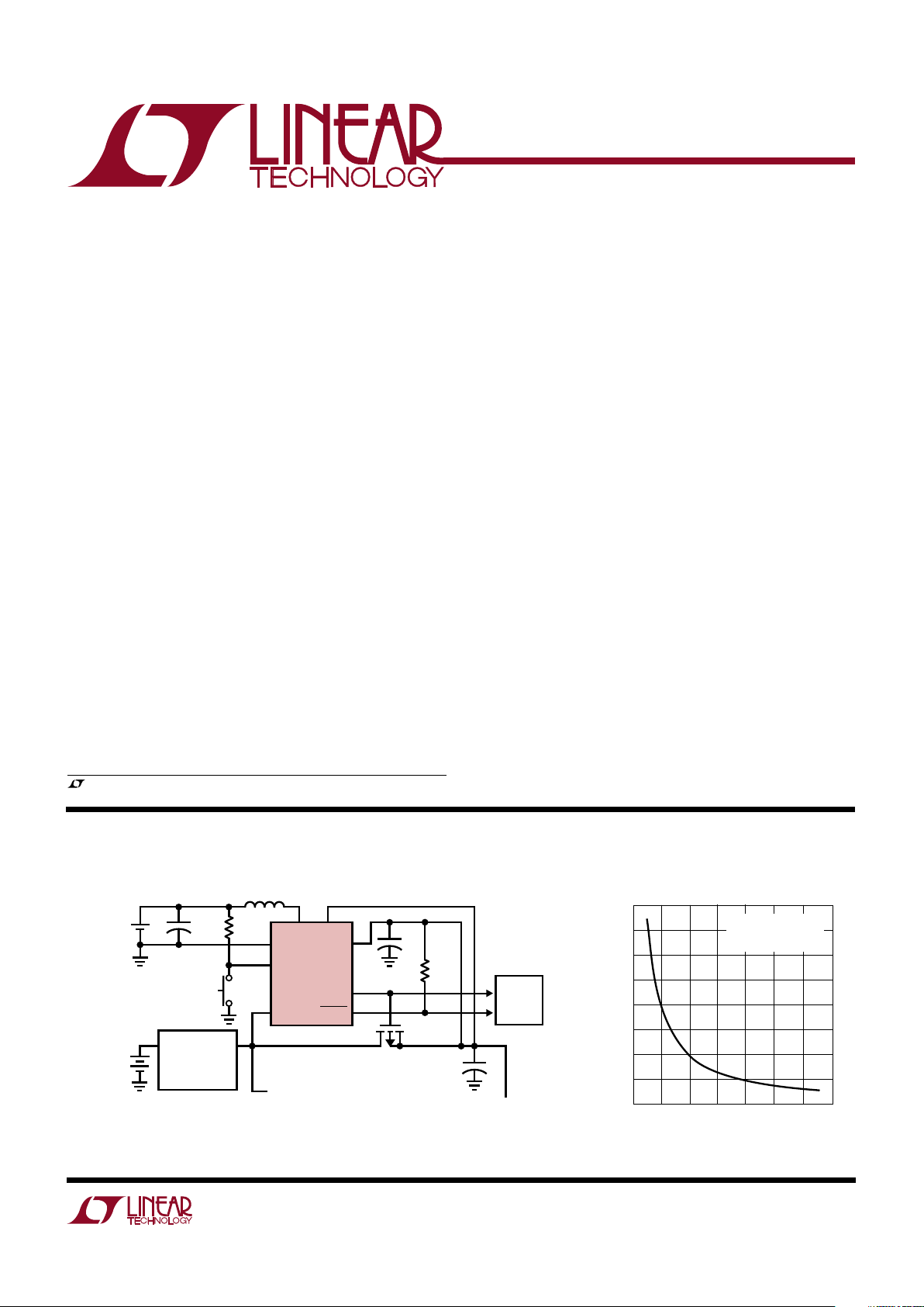
TYPICAL APPLICATION
U
CTL
C1
1µF
**BACKUP
BATTERY
1.2V
NiCd
MAIN
BATTERY
4.5V TO 28V
R1
68k
SW
LTC1559-3.3
*L1
22µH
GND
PS
7
1
8
5
6
3
S1
RESET
1559 TA01
2
4
V
BAK
V
CC
RESET
BACKUP
+
C3
100µF
10V
V
OUT
3.3V AT NORMAL MODE
3A
V
BAK
33mA (3.07V) AT BACKUP MODE
>33mA (3.3V) AT NORMAL MODE
C2
1µF
SYSTEM
µP
R2
100k
Q1
P-MOSFET
Si9424DY
* SUMIDA CD54-22µH
** PANASONIC P-11AAH
† CONSULT LTC1435 DATA SHEET FOR
APPLICATION CIRCUIT INFORMATION
†
LTC1435
SYNCHRONOUS
BUCK
REGULATOR
+
+
Backup Time vs
V
BAK
Output Load Current
V
BAK
LOAD CURRENT (mA)
0
BACKUP TIME (MINUTES)
800
700
600
500
400
300
200
100
0
15 25
1559 TA02
510
20 30 35
V
BAK
= 3.07V
NiCd CELL = P-11AAH
(110mA Hrs)
Page 2
2
LTC1559-3.3/LTC1559-5
ABSOLUTE MAXIMUM RATINGS
W
WW
U
(Note 1)
Terminal Voltages
VCC........................................................................ 6V
V
BAK
.................................................................... 12V
SW ...................................................................... 14V
All Other Pins .............................. – 0.3V to VCC + 0.3V
SW Input Currents ............................................. 500mA
V
BAK
Output Current ................... Short-Circuit Protected
Operating Ambient Temperature Range ....... 0°C to 70°C
Junction Temperature .......................................... 125°C
Storage Temperature Range .................. –65°C to 150°C
Lead Temperature (Soldering, 10 sec)...................300°C
ORDER PART
NUMBER
ORDER PART
NUMBER
S8 PART MARKING
LTC1559CS8-3.3
LTC1559CS8-5
ELECTRICAL CHARACTERISTICS
V
BAT
= 1.2V, TA = 0°C to 70°C unless otherwise noted.
LTC1559CGN-3.3
LTC1559CGN-5
LTC1559CS-3.3
LTC1559CS-5
Consult factory for Industrial and Military grade parts.
T
JMAX
= 125°C, θJA = 130°C/ W
1
2
3
4
8
7
6
5
TOP VIEW
S8 PACKAGE
8-LEAD PLASTIC SO
SW
GND
CTL
PS
V
BAK
V
CC
BACKUP
RESET
T
JMAX
= 125°C, θJA = 110°C/ W (GN)
T
JMAX
= 125°C, θJA = 110°C/ W (S)
TOP VIEW
S PACKAGE
16-LEAD PLASTIC SO
GN PACKAGE
16-LEAD PLASTIC SSOP
1
2
3
4
5
6
7
8
16
15
14
13
12
11
10
9
SW
SW
PGND
GND
CTL
SHDN
PS
NC
V
BAK
V
BAK
V
CC
BACKUP
RESET
RESET
NC
LOBAT
PACKAGE/ORDER INFORMATION
W
U
U
SYMBOL PARAMETER CONDITIONS MIN TYP MAX UNITS
Battery Backup Switching
V
CC
Operating Voltage Range LTC1559-3.3 ● 2.900 3.5 V
LTC1559-5 ● 4.400 5.5 V
V
BAT
Backup Battery Cell Voltage ● 1.0 1.2 1.5 V
I
VCC
Quiescent Supply Current (Note 2) ● 155 250 µA
I
BAT
Peak Inductor Current (Backup) Boost Converter in Low Current Mode (Note 7) ● 80 165 225 mA
Boost Converter in High Current Mode (Note 7) ● 225 330 445 mA
I
BAT(SHDN)
Battery Standby Current VCC = 0V ● 0.1 15 µA
I
VCC(SHDN)
Supply Current During Shutdown (Note 3) ● 50 µA
V
BAK(ON)VCC
Backup Request/Booster Assertion LTC1559-3.3 ● 3.011 3.070 3.127 V
Trip Point (Note 4) LTC1559-5 ● 4.475 4.625 4.775 V
V
BAK(OFF)VCC
Backup Deassertion Trip Point LTC1559-3.3 ● 3.061 3.119 3.176 V
(Note 4) LTC1559-5 ● 4.550 4.700 4.850 V
V
LOBAT1
Low V
BAT
Detect (Note 3) ● 0.95 1.00 1.05 V
V
UVLO(ON)VCC
UVLO Trip Voltage (Note 4) LTC1559-3.3 ● 2.904 3.003 3.102 V
LTC1559-5 ● 4.400 4.550 4.700 V
V
UVLO(OFF)VCC
UVLO Trip Voltage (Note 4) LTC1559-3.3 ● 3.061 3.119 3.176 V
LTC1559-5
● 4.550 4.700 4.850 V
155933
15595
Page 3
3
LTC1559-3.3/LTC1559-5
ELECTRICAL CHARACTERISTICS
V
BAT
= 1.2V, TA = 0°C to 70°C unless otherwise noted.
SYMBOL PARAMETER CONDITIONS MIN TYP MAX UNITS
UVLO Reset Monitor
V
LOBAT2VBAT
UVLO Trip Voltage (Note 5) ● 0.85 0.9 0.95 V
Backup Battery Charger
I
CHGF
Battery Charge Current During Fast Recharge ● 11 16 21 mA
I
CHGT
User-Programmable Trickle Charge ● 0.05 2 mA
Current Range
Q
RECH
Fast Recharge Factor (Note 6) 1.35 1.6 1.85 C/C
Q
TRK
Nominal Trickle Charge Multiplier Factor I
CHGT
= 1mA ● 8 10 12 A/A
V
CTL(CLAMP)
CTL Clamp Voltage in Trickle Mode I
CHGT
= 1mA ● 0.45 0.5 0.55 V
Push-Button Reset
V
CTL
CTL Input Threshold 250 mV
t
CTL
CTL Input Low Time (Debounce Time) 20 26 ms
Reset Timer
t
HRESET
Push-Button Duration for Hard Reset 1.10 1.8 3.4 sec
t
RST
RESET Pulse Width V
CTL
Low for <t
HRESET
(Soft Reset) ● 50 80 150 µs
V
CTL
Low for >t
HRESET
(Hard Reset) ● 115 185 345 ms
V
RST1
RESET Output Voltage VCC = 1V, I
SINK
= 10µA ● 5 200 mV
V
RST
RESET Output Voltage VCC = 4.25V, I
SINK
= 1.6mA ● 0.1 0.4 V
I
SC
RESET Output Current Output Source Current VCC = 3.3V 10 mA
Output Source Current VCC = 5V 20 mA
Short-Circuit Current Output Sink Current VCC = 3.3V 20 mA
Output Sink Current V
CC
= 5V 40 mA
PS Comparator
V
HYST
Comparator Threshold Hysteresis TA = 25°C90mV
Internal VCC Monitor Comparator
tr UVLO, Comparator Propagation Delay (Rising) 7.5 µs
Shutdown Pin (Note 3)
V
SHDN
SHDN Input Threshold Logic Low, V
IL
● 0.8 V
Logic High, V
IH
● 2V
I
SHDN
SHDN Pin Bias Current VCC = 5V, V
SHDN
= 0V ● 815 µA
The ● denotes specifications which apply over the full operating
temperature range.
Note 1: Absolute Maximum Ratings are those values beyond which the life of
a device may be impaired.
Note 2: Quiescent current is measured during push-button reset.
Note 3: Only applies to 16-pin version.
Note 4: Although the V
BAK(ON)
, V
BAK(OFF)
, V
UVLO(ON)
and V
UVLO(OFF)
threshold voltages have a specification tolerance, they are guaranteed by
design and tested in production never to overlap.
Note 5: Low cell voltage reset is only triggered when 0.25V < V
CTL
< 0.9V
for at least 20µs while in backup mode.
Note 6: Fast recharge factor is defined as the ratio of charge replenished to
the NiCd battery during fast recharge to the charge withdrawn from the
NiCd battery during backup.
Note 7: The LTC1559 switches automatically between the low and high
operating current levels. See Applications Information for more details.
Page 4
4
LTC1559-3.3/LTC1559-5
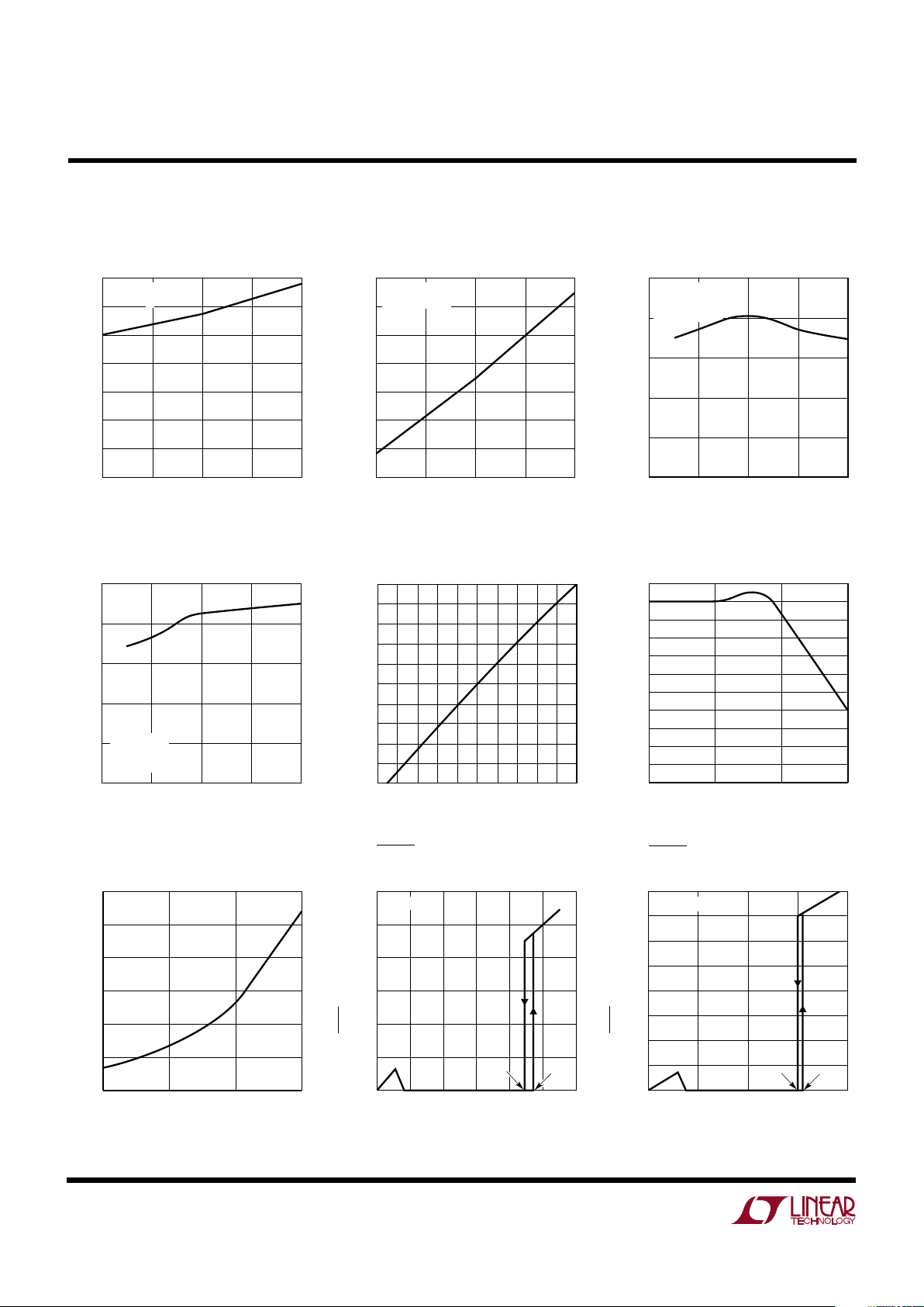
TYPICAL PERFORMANCE CHARACTERISTICS
UW
NiCd TERMINAL VOLTAGE (V)
1.0
OUTPUT POWER (mW)
140
120
100
80
60
40
20
0
1.1 1.2 1.3 1.4
1559 G01
IPK = 330mA
C
L
= 200µF
Output Power vs Battery Voltage
Boost Converter Switching
FrequencyBackup Time vs Battery Capacity
Normalized Fast Recharge
Current vs Temperature
Trickle Charge Multiplier Factor
Boost Converter Switching
Duty Cycle
TEMPERATURE (°C)
0
0.950
CURRENT RATIO (mA/mA)
0.960
0.970
0.980
0.990
25 50
1559 G06
75
1.000
0.955
0.965
0.975
0.985
0.995
1.005
Fast Recharge Time (Assume
NiCd Battery Fully Exhausted)
BATTERY CAPACITY (mA Hr)
64
0
TIME (HOURS)
10
20
30
40
60
128 256
1559 G07
512
50
RESET Output Voltage
vs Supply Voltage
SUPPLY VOLTAGE (V)
0
0
RESET VOLTAGE (V)
1
2
3
4
6
1
234
4.55V
1559 G08
56
5
4.7V
LTC1559-5
RESET Output Voltage
vs Supply Voltage
OUTPUT VOLTAGE, V
BAK
(V)
2
DUTY CYCLE (%)
40
60
10
1559 G04
20
0
4
6
8
100
80
LTC1559-3.3
V
BAT
= 1.2V
I
PK
= 330mA
NiCd CELL CAPACITY (mA Hr)
50
BACKUP TIME (HOURS)
3.5
3.0
2.5
2.0
1.5
1.0
0.5
0
125 250 375 500
1559 G02
V
BAT
= 1.2V
P
OUT
= 100mW
OUTPUT VOLTAGE, V
BAK
(V)
2
SWITCHING FREQUENCY (kHz)
50
75
10
1559 G03
25
0
4
6
8
125
100
LTC1559-3.3
V
BAT
= 1.2V
I
PK
= 330mA
NiCd BATTERY TRICKLE CURRENT (mA)
10.5
10.4
10.3
10.2
10.1
10.0
9.9
9.8
9.7
9.6
9.5
TRICKLE CHARGE FACTOR (mA/mA)
1559 G05
0 0.2 0.4 0.6
0.8
1.0
1.2 1.4 1.6 1.8 2.0
SUPPLY VOLTAGE (V)
0
RESET VOLTAGE (V)
4.0
3.5
3.0
2.5
2.0
1.5
1.0
0.5
0
1
234
3V
1559 G09
LTC1559-3.3
3.12V
Page 5

5
LTC1559-3.3/LTC1559-5
PIN FUNCTIONS
UUU
Pin Numbers Are Shown First for the SO-8 Package
Then the GN16 and S16 Packages
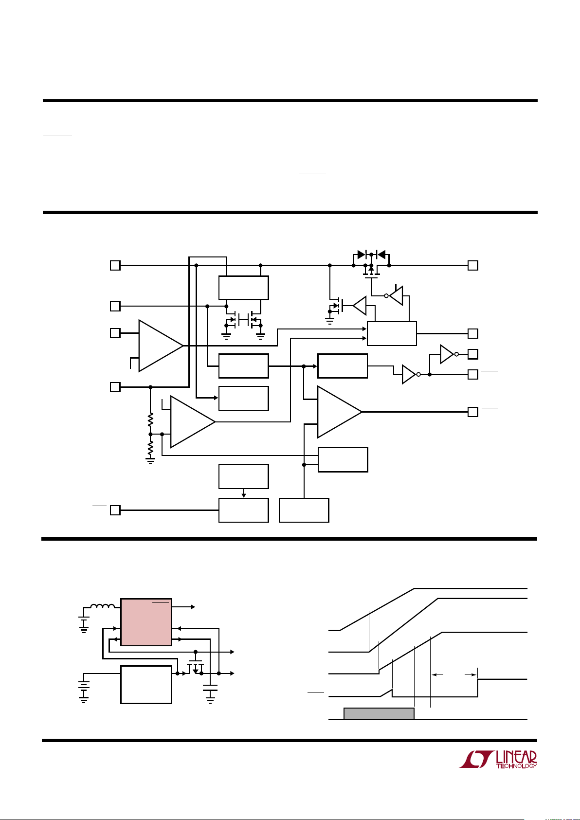
SW (Pins 1/1, 2): Boost Converter Switching Node. Con-
nect a 22µ H inductor from SW to the positive terminal of
the backup cell. In backup mode, this node is alternately
switched between ground and V
BAK
, generating the backup
output voltage. In fast or trickle charge mode, an internal
regulator outputs a constant DC current from this pin
through the 22µH inductor and into the NiCd battery.
During power-up or undervoltage lockout (UVLO), the SW
pin enters a high impedance state.
GND (Pins 2/4): System Ground. The low power internal
circuitry returns to this pin in the 16-pin packages. GND
and PGND are bonded together to this pin in the 8-pin
package.
CTL (Pins 3/5): Control. This pin provides three functions.
In backup mode this pin is a high impedance input and
monitors the backup battery cell voltage (V
BAT
). If V
BAT
drops below 0.9V, the LTC1559 enters UVLO. During
trickle charge mode, an external resistor R
EXT
sets the
trickle charge current. In all modes, pulling the CTL pin
below 250mV generates either a “soft” or “hard” reset
pulse. See the Applications Information section for more
information.
PS (Pins 4/7): Power Supply Sense. This pin senses the
presence of the main supply and triggers the LTC1559 to
terminate backup mode. During backup, VCC is driven
externally by the LTC1559’s boost convert’s output (V
BAK
).
When PS > VCC during backup, the LTC1559 pulls down
the BACKUP pin, reconnecting the system regulator output to the system VCC. The PS pin is needed in applications
that use a P-channel MOSFET (driven by the BACKUP
signal) to isolate the system regulator during backup. If
not needed, PS can be disabled by tying it to ground.
RESET (Pins 5/11): System Reset, Active Low. This is an
open-drain output. This pin provides a low going reset
signal to the system processor. A 200ms pulse is generated if the CTL pin is pulled low for more than two seconds
(“hard” reset) or if the LTC1559 comes out of UVLO. This
“hard reset” stops the internal boost converter if it is
running. This pin is held low if the LTC1559 is in UVLO and
is guaranteed to be valid when VCC is greater than or equal
to 1V.
RESET also provides a low going 100µ s signal whenever
the CTL pin is pulled low for less than two seconds (“soft”
reset). Unlike hard reset, soft reset does not affect the
LTC1559’s current operating mode.
BACKUP (Pins 6/13): System Backup Signal. This is a
TTL-compatible output driver that pulls low unless the
LTC1559 is in backup mode. BACKUP signals the system
controller that the system is in backup mode so that it can
reduce system loading. BACKUP can also be used to drive
the gate of a P-channel MOSFET in series with the main
system regulator’s output. See the Applications Information section for more details.
VCC (Pins 7/14): Power Supply Input. All internal circuits
except the boost converter are powered from this pin. A
0.1µF bypass capacitor is required from VCC to ground.
The UVLO detector inside the LTC1559 monitors VCC. If
VCC drops below the rated output voltage by 9%, the
LTC1559 enters UVLO mode and RESET is asserted. The
LTC1559-3.3 exits UVLO if VCC rises to greater than
–5.5% of the rated output voltage. The LTC1559-5 exits
UVLO if VCC rises to greater than –6% of the rated output
voltage. See the Applications Information section for more
details.
V
BAK
(Pins 8/15, 16): Backup Supply Output. The LTC1559’s
boost converter provides the regulated output voltage to
the system through V
BAK
during backup mode.
16-Pin GN and SO Packages
PGND (Pin 3): Power Ground. The internal driver circuitry
returns to this pin. PGND should be connected to a low
impedance ground plane in close proximity to the NiCd
battery cell.
SHDN (Pin 6): Chip Shutdown. A TTL-compatible active
low voltage at SHDN puts the LTC1559 into low power
shutdown mode. In shutdown, all internal circuits power
down and are held in a reset state. The SW, CTL and V
BAK
pins enter into high impedance states. In shutdown mode,
supply current drops to below 50µA and current drawn
from the backup cell drops to below 15µA.
Page 6
6
LTC1559-3.3/LTC1559-5
LOBAT (Pin 9): Low Backup Battery Detector Output. This
is an open-drain output with an internal weak pull-up. It is
asserted if the NiCd cell terminal voltage drops below
1.0V. This pin is pulled high if the LTC1559 is in trickle
charge mode.
PIN FUNCTIONS
UUU
1559 SW01
V
BAT
MAIN
BATTERY
C
OUT
BACKUP
SYSTEM
V
CC
1.2V
NiCd
SW
22µH
LTC1559
RESET
PS
Q
EXT
V
BAK
V
CC
BACKUP
TO
SYSTEM
CONTROL
V
IN
FOR MORE DETAILED CIRCUIT APPLICATION SCHEMATICS,
PLEASE REFER TO THE TYPICAL APPLICATIONS SECTION
MAIN SYSTEM
REGULATOR
V
OUT
V
BAT
BACKUP
RESET
V
CC
PS
1559 SW02
200ms
RATED BATTERY TERMINAL VOLTAGE
RATED V
CC
VOLTAGE
–5.5% (LTC1559-3.3)
–6% (LTC1559-5)
1
2
3
4
Cold Power Boot-Up (Main Battery Replaced/Turned On)
Simplified LTC1559 Connections in a Battery Backup System
SWITCHING WAVEFORMS
UW
–
+
LEVEL SENSE
AND DEBOUNCE
THERMAL
LIMIT
SHUTDOWN
LOGIC
BANDGAP
V
REF
= 1.272V
CHARGER
RESET
GENERATOR
BOOST/BACKUP
LOGIC
GAS GAUGE
V
REF
V
REF
V
CC
SHDN
PS
RESET
N1
P1
V
BAK
VCC/V
BAK
CTL
SW
–
+
–
+
UVLO
DETECTOR
RESET
BACKUP
LOBAT
1559 BD
BLOCK DIAGRAM
W
RESET (Pin 12): System Reset, Active High. This is a TTLcompatible output driver. It can connect to systems that
require active high logic. The RESET output will go high if
RESET is pulled low.
Page 7

7
LTC1559-3.3/LTC1559-5
SWITCHING WAVEFORMS
UW
Cold Power Boot-Up Description
1. System regulator starts to ramp up the output (PS)
once the V
BAT
voltage increases beyond the minimum
input value.
2. VCC starts to increase once PS is high enough to turn on
Q
EXT
’s body diode. RESET is asserted when VCC is less
than or equal to 1V.
3. The LTC1559’s internal bandgap wakes up. Q
EXT
turns
on and VCC = PS. The LTC1559’s internal boost converter does not turn on as RESET remains asserted.
4. RESET is asserted for a further 200ms after VCC reaches
–5.5% of its rated VCC value for the LTC1559-3.3 and
–6% of its rated VCC value for the LTC1559-5.
Backup Mode (Main Battery Discharged)—
LTC1559-3.3
INDUCTOR
CURRENT
RESET
BACKUP
V
CC
V
NiCd
LOBAT
1559 SW03
t
r
t
r
–7%
1.2V
–7%
–7%
1V
0.9V
–5.5%
BOOST CONVERTER OUTPUT
t
f
t
r
t
r
(4)(3)(2)(1)
“1”
“1”
Backup Mode Description
1. Trigger into Backup Mode. Main battery fails and V
CC
drops 7% below the rated value. The backup pin is
asserted after a tr delay time and the boost converter is
turned on.
2. Backup Mode. The LTC1559’s boost converter charges
and discharges the inductor with 165mA peak current.
If VCC doesn’t increase above VCC(rated value) – 7%
(due to a heavy load), the boost converter increases
peak charging current to 330mA. If VCC rises above
VCC(rated value) – 7%, the boost converter stops and
the backup pin remains asserted.
3. Recovery from Backup Mode. While the boost converter is running, the main battery is restored. This
causes the system regulator to increase PS above VCC.
When PS > VCC or VCC > VCC(rated value) –5.5%, the
BACKUP pin deasserts and the boost converter finishes
its last cycle.
4. Trigger into UVLO. During backup, the 1.2V NiCd cell is
discharged and its terminal voltage falls. The LOBAT pin
is asserted to give an early warning if the cell voltage
drops below 1V. RESET is asserted when the cell
voltage drops below 0.9V and the LTC1559 enters
UVLO mode.
Page 8

8
LTC1559-3.3/LTC1559-5
APPLICATIONS INFORMATION
WUU
U
Overview
The LTC1559 is a versatile backup battery control system
designed to provide all the functions necessary to implement a complete, highly integrated backup system within
a single chip. It allows the system to maintain its rated
supply voltage during backup, offering maximum system design flexibility. The LTC1559 allows the use of a
low cost rechargeable NiCd cell for backup, eliminating
the need for expensive, replaceable 4.5V lithium backup
cells.
The LTC1559 includes an onboard boost converter
designed to generate a fixed voltage (3.07V for 3.3V parts
and 4.625V for 5V parts) from a single 1.2V NiCd cell.
When connected to the system DC/DC converter’s output,
the LTC1559 enables the system connected to the VCC rail
to continue operation when the main power supply fails. A
“smart” recharging circuit uses an accumulating gas
gauge to measure the charge extracted from the backup
battery during a backup cycle. This measured charge is
then replaced in a fast recharge cycle, without wasting
excess power or overcharging the backup cell. An externally adjustable trickle charge circuit maintains the cell
charge after the fast charge cycle has completed, minimizing drain from the main battery during standby.
Included in the LTC1559 is a complete backup circuit that
monitors the main system power and automatically
switches in the backup circuit as the primary power supply
falls away (due to a weak or disconnected main battery).
The LTC1559 also performs VCC supervisory functions
during normal system operations. An LTC1559-3.3
monitors a 3.3V supply voltage at its VCC pin while an
LTC1559-5 monitors a 5V supply at its VCC pin. In both
cases, the LTC1559 derives power for the majority of the
internal circuitry (except for the boost converter) from its
VCC pin. Table 1 shows the signal conditions for the
various operating modes of the LTC1559-3.3. Table 2
shows the signal conditions for the various operating
modes of the LTC1559-5.
Table 1. LTC1559-3.3 Operating Modes
OPERATING MODES CONDITIONS
UVLO Reset 1V < VCC < VCC(rated value) – 9% or
V
BAT
< 0.9V
Push-Button Reset V
CTL
< 250mV
UVLO Reset Recovery VCC > VCC(rated value) – 5.5%
Backup Mode Activation VCC < VCC(rated value) – 7%
Backup Mode Exit VCC > VCC(rated value) – 5.5%
or PS > V
CC
Boost Converter Activation VCC < VCC(rated value) – 7%
Boost Converter Deactivation VCC > VCC(rated value) – 7%
Table 2. LTC1559-5 Operating Modes
OPERATING MODES CONDITIONS
UVLO Reset 1V < VCC < VCC(rated value) – 9%
or V
BAT
< 0.9V
Push-Button Reset V
CTL
< 250mV
UVLO Reset Recovery VCC > VCC(rated value) – 6%
Backup Mode Activation VCC < VCC(rated value) – 7.5%
Backup Mode Exit VCC > VCC(rated value) – 6%
or PS > V
CC
Boost Converter Activation VCC < VCC(rated value) – 7.5%
Boost Converter Deactivation VCC > VCC(rated value) – 7.5%
Boost Converter Operation
The LTC1559 uses an onboard boost converter with a
fixed peak current architecture that provides a simple and
flexible system solution while eliminating the need for
conventional frequency compensation. The boost
converter’s output, set to 93% (LTC1559-3.3) or 92.5%
(LTC1559-5) of the rated VCC, supports the system V
CC
during backup. It supplies a minimum backup power of
100mW. The boost converter operates in a modified
pulse-skipping mode; each switch cycle transfers a known
amount of charge from the backup cell to the regulated
output. This prevents uncontrolled discharge of the backup
cell and allows the LTC1559 to accurately measure the
charge removed from the backup cell by counting the
charge pulses.
The LTC1559 enters backup mode when the main battery
voltage drops and causes VCC, the system regulator’s
output, to fall. As shown in Figure 1, VCC is scaled down
by an internal resistor divider and fed to the LTC1559’s
backup comparators. These compare the scaled voltage
Page 9

9
LTC1559-3.3/LTC1559-5
APPLICATIONS INFORMATION
WUU
U
ferred for the first two consecutive switch cycles. If V
CC
falls below
V
CC
(rated value) –7% (LTC1559-3.3)
, the
boost operation starts by connecting the SW pin internally
to ground through an internal 0.5Ω N-channel MOSFET
(N1 in the Block Diagram). The current through the external 22µH inductor rises linearly through this switch.
When the switch current reaches an internally preset level
of 165mA, the boost converter connects the SW pin to the
V
BAK
pin through an internal 2Ω P-channel MOSFET. The
inductor current discharges through the P-channel (P1 in
the Block Diagram) and charges up the system’s V
CC
capacitor (C
OUT
of the system regulator, Figure 1). The
inductor current falls at a rate proportional to the difference between the backup cell voltage and the output
voltage V
BAK
. When the inductor current reaches zero,
indicating all of its energy has been transferred to the
output capacitor, the LTC1559 monitors the VCC voltage.
If VCC has increased above the
V
CC
(rated value) –7%
(LTC1559-3.3)
threshold, the boost converter shuts off
both switches and waits for VCC to drop below
V
CC
(rated
value) –7% (LTC1559-3.3)
again.
with an internal trimmed V
REF
(1.272V), switching the
LTC1559 into backup mode if VCC drops 7%
(LTC1559-3.3) or 7.5% (LTC1559-5) below its rated
value. Upon entering backup mode, the BACKUP pin is
asserted and the internal boost converter turns on. The
BACKUP signal turns off the external P-channel MOSFET
(if used), isolating the system regulator from the LTC1559.
The boost converter charges the VCC capacitor, C
OUT
, of
the system regulator until VCC rises above V
CC
(rated
value) – 7% (LTC1559-3.3) or VCC (rated value) – 7.5%
(LTC1559-5).
Once VCC rises above
V
CC
(rated value) – 7% (LTC1559-
3.3)
, the boost converter deactivates and the freshly
charged VCC capacitor C
OUT
supplies power to the system.
The cycle repeats again when the VCC capacitor’s charge
is drained away and VCC again drops below
V
CC
(rated
value) – 7% (LTC1559-3.3)
. The BACKUP pin remains
asserted until the main battery is restored. This ensures
that the LTC1559 does not switch in and out of backup
mode unnecessarily.
The LTC1559’s boost converter minimizes output ripple
under light load conditions by reducing the charge trans-
Figure 1. Typical LTC1559 Connection
+
BOOST
CONVERTER
SYSTEM
REGULATOR
LTC1559
R1
PS
V
CC
R2
1559 F01
BACKUP
LOGIC
V
REF
BACKUP
SYSTEM
V
CC
V
BAK
C
OUT
LIGHT CURRENT MODE
165mA
(PEAK)
330mA
(PEAK)
HEAVY CURRENT MODE
1559 F02
Figure 2. Inductor Current During Switching
Figure 3. V
BAK
Ripple
1
BOOST
CYCLE
V
BAK
ESR RIPPLE
DISCHARGE
PERIOD
t
DISCH
CHARGE
PERIOD
t
CH
1559 F03
Page 10

10
LTC1559-3.3/LTC1559-5
If VCC is still less than
V
CC
(rated value) –7% (LTC1559-
3.3)
after the first boost cycle, the LTC1559 immediately
reconnects SW to ground, repeating the boost cycle. If
after two consecutive pulses, VCC is still not above the
boost threshold
V
CC
(rated value) –7% (LTC1559-3.3)
,
the LTC1559 decides that the load is not so light after all,
and doubles the internal inductor charging current limit to
330mA for subsequent cycles. This is high current mode.
By doubling the peak inductor current, each boost cycle
effectively carries four times more energy compared to
low current mode (E = 1/2 • LI2), doubling the available
output power. When VCC exceeds the
V
CC
(rated value)
–7% (LTC1559-3.3)
boost threshold, the LTC1559 stops
the boost converter and resets the internal 2-pulse counter.
The next time VCC falls below
V
CC
(rated value) –7%
(LTC1559-3.3)
, the boost converter restarts in low current
mode for at least two boost cycles. Moderate or changing
loads cause the LTC1559 to shift between the two peak
inductor current limits, keeping the output in tight regulation. Near its maximum load capability, the LTC1559 will
stay in 330mA high current mode and the output voltage
V
BAK
will hover around
V
CC
(rated value) –7%
(LTC1559-3.3)
.
VCC Capacitor ESR
The type of output capacitor and the rated VCC value will
affect the LTC1559’s output ripple and efficiency. In most
applications, the VCC capacitor is primarily determined by
the requirements of the main power supply. Such a
capacitor will generally meet the requirements of the
LTC1559. In unusual circumstances or circuits where
the main system VCC capacitor is located some distance
away from the LTC1559, a local output capacitor may be
necessary.
The ripple on the VCC pin is equal to the capacitor ESR
voltage drop due to the boost converter’s output current
pulses. The ripple frequency and output duty cycle is
proportional to the inductor discharge time. Given a fixed
inductor value (22µ H) and a known peak current limit, the
booster’s discharge time in each boost cycle is proportional to the difference between V
BAK
(93% of the rated V
CC
for the LTC1559-3.3 and 92.5% of the rated VCC for the
LTC1559-5) and the battery cell voltage, V
BAT
(1.2V).
APPLICATIONS INFORMATION
WUU
U
Assuming ESR = 0.2Ω, I
IND(PEAK)
= 330mA, VCC = 5V,
V
RIPPLE(P-P)
= (I
IND(PEAK)
)(R
ESR(CAP)
)
= (330mA)(0.2Ω)
= 66mV
Since VCC must be scaled down internally, the external
resistor ratio:
= 5V/1.272V
= 3.931
Therefore the ripple seen by the VCC comparators is:
= 66mV/3.931
= 16.79mV
The discharge time period,
t
DISCH
= (L • I
IND(PEAK)
)/(V
BAK
– V
BAT
)
= (22µH • 330mA)/(4.625 – 1.2V)
= 2.12µs
For VCC = 3.3V and I
IND(PEAK)
= 330mA,
V
RIPPLE(P-P)
= 66mV
RB resistor ratio = 3.3/1.272 = 2.594
Ripple voltage = 25.4mV
t
DISCH
= 3.9µs
The internal VCC comparators are designed to have a slow
response time to filter away this ripple. The V
CC
(rated
value) – 5.5% (LTC1559-3.3) and VCC(rated value) – 9%
comparators have a 6µs rising edge delay and 2µs falling
edge delay. The V
CC
(rated value) – 7% (LTC1559-3.3)
comparator has a similar 6µ s rising time delay but a much
longer falling time delay of 20µs. This enables the com-
parator to control the boost converter properly, and avoids
turning off the boost converter prematurely due to false
triggering by the ESR ripple.
Exit from Backup
When a main battery is inserted into the system, the
LTC1559 follows a specific sequence to exit backup mode
and return control to the main supply. The sequence
depends on the type of main power supply used. In
systems where the main supply’s output impedance is
Page 11

11
LTC1559-3.3/LTC1559-5
APPLICATIONS INFORMATION
WUU
U
to the load while charge on the V
CC
capacitor drains away.
If VCC drops below VCC (rated voltage) – 9% for more than
7.5µ s, the LTC1559’s VCC supervisory circuit activates
UVLO mode, shutting off the boost converter and asserting the Reset pins. The 7.5µ s delay prevents the LTC1559
from being fooled by brief transients or noise spikes on its
VCC pin. Upon receipt of the reset signal, the host system
should shut down in an orderly manner. The LTC1559’s
VCC supervisory circuit will remain alive until VCC is less
than 1V to ensure a valid RESET pin signal.
Backup Cell Voltage Monitoring
As the boost converter removes charge from the backup
NiCd cell, the cell’s terminal voltage falls. Permanent
damage to the NiCd cell can occur if it is discharged to
below 0.9V. To prevent this, the LTC1559 monitors the
cell’s terminal voltage through the CTL pin during backup.
If the CTL pin drops below 0.9V for more than 20µs, the
UVLO circuit shuts down the boost converter and asserts
the RESET and RESET pins. Since the CTL pin can also be
connected to an external push-button reset, the LTC1559
includes internal logic to ensure that the low cell voltage
reset is triggered only if the CTL pin is between 0.9V and
0.25V. This will prevent a push-button reset (which pulls
CTL below 250mV) from being mistaken as a low cell
voltage condition. Unusual situations where the NiCd cell
voltage drops drastically below 0.25V will also trigger
UVLO, since the LTC1559 will treat this as a “hard” reset
after two seconds.
An optional LOBAT output, available in the 16-pin GN or SO
package, can be used to signal the system if the cell
voltage falls below 1V, giving an early warning that the
backup cell is heavily discharged. The LOBAT pin is
disabled if the LTC1559 is in trickle charge mode,
because the CTL pin is regulated to 0.5V by the LTC1559.
Fault Protection and Thermal Limit
The LTC1559’s boost converter incorporates two internal
timers that turn off the switch transistors if the inductor
charge or discharge time gets abnormally long.
The inductor charge time may get abnormally long if the
NiCd cell voltage drops below 0.25V without triggering the
0.25V < V
BAT
< 0.9V low cell voltage comparator. In this
high when inactive (typically a boost regulator with an
output catch diode), the LTC1559 detects the return of the
main supply by watching for VCC to exceed V
CC
(rated
value) – 5.5% (LTC1559-3.3). The LTC1559 then shuts
down its internal boost converter and begins to recharge
the NiCd cell. In such applications, the PS pin is not used
and can be tied to ground. No external P-channel MOSFET
is required to isolate the main supply from the system V
CC
during backup.
In systems where the main supply’s output impedance is
low when inactive (typically buck regulators), the main
supply must be disconnected from the system VCC during
backup to prevent the inactive supply from loading the
LTC1559. This is typically accomplished using an external
P-channel MOSFET as shown in Figure 1. When the main
supply is restored, the P-channel MOSFET’s body diode
forward-biases. This allows current to flow into the system VCC, but the forward drop across this diode may
prevent VCC from reaching the V
CC
(rated value)
– 5.5% (LTC1559-3.3) threshold that deactivates the
LTC1559’s backup mode. In such systems, the PS pin
should connect directly to the output of the main system
supply. When the system regulator’s voltage rises about
2.5% above the backup VCC, the PS comparator triggers
and causes the LTC1559 to deassert the BACKUP pin
signal. This signals the system controller to restore system loading and resume normal operation. At the same
time, the external P-MOSFET is driven by the BACKUP
signal. The P-channel MOSFET turns on and allows the
main regulator to bypass its body diode and drive the
system VCC directly.
Since the user can replace the main battery anytime during
the LTC1559’s backup operation, the BACKUP signal may
be deasserted while the boost converter is switching. To
prevent the potential problem of residual energy in the
inductor, the LTC1559 will only stop the boost converter
after it completes the current boost converter cycle.
UVLO Under Excessive Backup Load
Very heavy loads (above the LTC1559’s maximum power
output) will pull the boost converter’s output below the
boost threshold. Under these conditions, the LTC1559’s
boost converter continues to supply 330mA current pulses
Page 12

12
LTC1559-3.3/LTC1559-5
case, the NiCd cell is assumed to be damaged and the
LTC1559’s priority is shutting down the system gracefully. In this case, the timer will shut off the N-channel
switch transistor after a maximum charging time (14µs).
The boost converter continues switching but delivers
reduced output power, causing VCC to drop. The LTC1559
enters UVLO if VCC drops below VCC(rated value)
– 9% or if the LTC1559 detects that CTL is lower than
0.25V for two seconds, in which case “hard” reset occurs.
The discharge time can also get abnormally long if a
serious overload condition occurs during switching. The
timer shuts off the P-channel pass transistor after 10µs,
protecting the boost converter. The LTC1559 enters UVLO
as VCC drops below VCC(rated value) – 9%.
In addition, the LTC1559 has safe area operation protection with an internal thermal shutdown circuit. If the device
is overloaded for a long period of time, the thermal
shutdown circuit forces the LTC1559 into UVLO. The
threshold temperature for thermal shutdown is typically
155°C.
The LTC1559’s boost converter is designed so that no
current drains from the battery to the load during output
short circuit or VCC = 0V conditions. This assures that the
system can be powered down for a long period of time.
This eliminates the risk of finding a nonfunctioning backup
system upon power-up.
Backup Cell Fast Recharge
The LTC1559 includes an onboard gas gauge circuit,
consisting of a 23-bit divider and a 9-bit up/down counter.
The gas gauge logic assumes that the boost converter
uses a 22µH inductor, allowing it to accurately measure
battery charge by counting pulses. The gas gauge counts
up from zero as charge is removed from the backup cell in
backup mode. It takes 8.4 million 165mA boost pulses
(low current mode) to increment the up/down counter by
one count. In high current mode, the 330mA pulses skip
the first two bits of the divider because each 330mA pulse
carries four times as much energy as a 165mA pulse. At
maximum load and VCC = 4.625V (LTC1559-5), the gas
gauge counter will increment by one count every 7.5µs
while the boost converter is running. Full count is reached
APPLICATIONS INFORMATION
WUU
U
after approximately 2.2 hours, equivalent to about
512mAhr of charge.
Upon entering recharge mode (after the main battery is
restored) the LTC1559 connects a 16mA fast recharge
current source from VCC to the SW pin. At the same time,
an internal free running oscillator counts down the gas
gauge counter at a rate designed to typically replace 160%
of the charge previously removed from the backup cell.
When the gas gauge counter reaches zero, the LTC1559
reduces the charging current at the SW pin to the userprogrammed trickle charge current level.
Under some circumstances, the LTC1559 can exit backup
mode with invalid gas gauge contents. This occurs under
three possible conditions:
1. The backup cell was completely exhausted during a
backup cycle and the LTC1559 entered UVLO.
2. The backup cell was replaced while the main supply was
disabled.
3. A backup cycle was terminated prematurely by a “hard”
reset or an output overload.
In these cases, the LTC1559 assumes that the backup cell
is exhausted and presets the gas gauge counter to a
default capacity of 128mAhr. It then initiates a recharge
cycle.
Setting the gas gauge to this default value results in a fast
recharge cycle long enough to replenish 1.6 times
128mAhr into the backup cell (13.9 hours). If the backup
cell is actually exhausted, it will be fully recharged. If the
battery is partially or fully charged, or is significantly
smaller than 128mAhr capacity, the extra charging time is
wasted. However, the LTC1559’s 16mA fast charge current is not high enough to damage the cell. Once the fullcount recharge has been completed, the backup cell is
assumed to be fully charged and subsequent backup/
recharge cycles resume normally.
Although the LTC1559 will not fully recharge backup cells
larger than 128mAhr capacity upon power-up, it can still
be used with such cells. Such a cell will be fully replenished
by the subsequent trickle charge cycle. Under most conditions, even a partially charged large cell will still be
capable of supporting several hours of backup. For
Page 13

13
LTC1559-3.3/LTC1559-5
APPLICATIONS INFORMATION
WUU
U
example, a small 60mAhr SAFT cell can back up the
system for 20 minutes at an output power of 100mW. Note
that at VCC = 3.07V (LTC1559-3.3), the boost converter
efficiency improves and allows more backup time from the
same cell compared to VCC = 4.625V (LTC1559-5).
Once it reaches full recharge, a cell bigger than 512mAhr
will overrun the gas gauge counter before it runs out of
charge during an extended backup cycle. The LTC1559
gas gauge counter will not roll over if this occurs; it will
stay at full count until the backup cycle ends and then
partially recharge the cell with a full count cycle as above.
Very short backup cycles (<32s) may not extract enough
charge from the backup cell to increment the gas gauge
counter at all. To ensure that the backup cell is not slowly
“nibbled” away, the gas gauge counter is always
incremented by 1mAhr each time the controller exits
backup. This ensures that the backup cell is replenished
with at least a 1mAhr charge every time the LTC1559
enters backup mode.
Battery Backup Cell Trickle Charge
When the gas gauge counter reaches zero, the LTC1559
terminates fast recharge and reduces the recharge current
to the user-programmed trickle current level. The LTC1559
provides a trickle current that the user can program from
50µ A to 2mA. The trickle current is set by an external
resistor from the positive terminal of the backup cell to the
Figure 4. Trickle Current Charger
R
EXT
V
CC
1µF
I
10I
1.2V
NiCd
CELL
SW
CTL
0.5V
1559 F04
11×1×
LTC1559
+
–
+
+
–
CTL pin. In trickle charge mode, CTL is regulated to 0.5V,
resulting in a CTL pin current of (V
BAT
– 0.5)/R
EXT
. This
current is internally multiplied to feed back ten times the
R
EXT
current into the backup battery. Since the LTC1559
trickle charges only after the completion of the fast
recharge cycle, the backup cell voltage should be very
close to 1.2V. This simplifies the calculation of the R
EXT
resistor value. For example, a 47k resistor from V
BAT
to
CTL sets the trickle charge current to 150µA.
Undervoltage Lockout
The LTC1559 includes an undervoltage lockout (UVLO)
circuit that shuts the system down gracefully if the backup
cell is exhausted or overloaded. As described in the
previous section, the LTC1559 terminates backup operation and remains off until the main power supply returns.
It then runs a fast recharge cycle to recharge the backup
cell. An onboard low-battery comparator in the 16-pin GN
or SO package provides an early warning signal if the
backup cell drops below 1V.
The UVLO circuit trips if the LTC1559’s VCC supervisory
circuit detects that VCC drops below –9% of the rated V
CC
voltage due to overload or output short-circuit conditions.
Once the UVLO circuit trips, the LTC1559 asserts the
RESET and RESET pins until the VCC voltage drops below
1V. It then remains off until VCC rises to within –5.5% of
the rated output voltage (LTC1559-3.3). During power-up
from UVLO, the LTC1559 asserts the RESET and RESET
pins until the VCC(rated value)–5.5%(LTC1559-3.3)
threshold. Once VCC exceeds VCC(rated value) – 5.5%
(LTC1559-3.3), the RESET and RESET pins remain
asserted for another 200ms (“hard” reset) before being
released to inform the system to start operating.
Reset Operation
The LTC1559 includes an onboard push-button reset
switch controller. If the CTL pin is pulled to ground
(<250mV) by a push-button or an open-drain output, the
LTC1559 generates a pulse at the RESET and RESET pins
after the trailing edge of the CTL signal. A short (less than
two seconds) low going signal at CTL generates a “soft”
reset (100µ s) pulse at the reset pins. A low CTL signal for
more than two seconds generates a “hard” reset pulse at
the RESET and RESET pins. During “hard” reset, the
Page 14

14
LTC1559-3.3/LTC1559-5
APPLICATIONS INFORMATION
WUU
U
shut off completely. Note that the backup cell slowly
discharges through R
EXT
in this mode.
Inductor Selection
The LTC1559 is designed to operate with a recommended
inductor value of 22µ H (±20%) with < 0.2Ω DC resistance.
Using inductor values above 22µ H will deliver more output
power but will cause the gas gauge counter to count
inaccurately and under-recharge the backup cell. At the
same time, the N-channel transistor timer will limit the
peak current if the charging time becomes overextended
due to the higher inductor value. Using inductor values
lower than 22µ H will degrade the boost converter’s maximum output power and cause the gas gauge counter to
overcharge the backup cell. Table 3 lists a few recommended surface mount inductor part numbers.
Table 3. Recommended Inductors
PART TYP INDUCTOR DCR
MANUFACTURER NUMBER VALUE (Ω)
Sumida CD54-220 22µH ±20% 0.18
Sumida CDRH73/74 22µH ±20% 0.2/0.11
Capacitor Selection
The LTC1559 requires a VCC capacitor of 100µ F to ensure
that boost converter can regulate the output under maximum load conditions. The capacitor’s ESR should be
small (<0.2Ω) to minimize voltage spikes that might
incorrectly trigger the LTC1559’s internal VCC comparators. Note that the LTC1559 can usually share the output
capacitor with the system regulator. However, a 1µF is
recommended directly at the LTC1559’s VCC pin. The V
CC
capacitor’s ratings like V
MAX
, I
RIPPLE(RMS)
all must meet
the system regulator’s specifications as well.
Battery Selection
A primary application for the LTC1559 is a “bridging”
supply, only providing backup current while the main
system battery is being replaced. In these applications,
the LTC1559 works well with NiCd button cells or small
cylindrical cells, reducing system costs and board space.
It is optimized for use with up to 512mAhr battery
capacities.
Figure 5. Push-Button Resets
CTL
RESET
(A)
0V
0V
0V
20ms
DEBOUNCE
(B)
>0.25V
t
CTL
< 20ms
20ms < t
CTL
< 2s
>0.25V
“SOFT” PUSH-BUTTON RESET AT CTL
(A) CTL < 0.25V FOR LESS THAN 20ms
(B) CTL > 0.25V FOR MORE THAN 20ms
“HARD” PUSH-BUTTON RESET AT CTL
CTL < 0.25V FOR MORE THAN 2s
20ms DEBOUNCE AT FALLING AND RISING RESET EDGE
100µs 100µs
CTL
1559 F05
RESET
CTL
RESET
200ms
2s
t
CTL
> 2s
20ms
20ms
LTC1559 disables the boost converter if it is in backup
mode. All signals at the CTL pin are debounced for 20ms
to prevent multiple resets, allowing the CTL pin to be
connected directly to a push-button to ground.
The RESET pin is an open-drain output that requires an
external pull-up resistor. The RESET pin is a TTL compatible CMOS output.
Shutdown
The 16-pin LTC1559 has a TTL compatible input, SHDN
that shuts down the whole chip, asserts the RESET and
RESET pins and places the CTL, V
BAK
and SW pins into
high impedance states. The SHDN pin has an internal pullup of 8µ A that ensures the chip will not shut down if the pin
is left floating. The chip consumes less than 50µA during
shutdown.
Although there is no SHDN pin for the SO-8 package, the
user can shut down the part by pulling CTL to ground. The
chip enters “hard” reset leaving only the bandgap and
comparators alive. The charger and the boost converter
Page 15

15
LTC1559-3.3/LTC1559-5
The LTC1559 works with standard or memory backup
specific NiCd cells. Memory backup cells can operate at
higher temperatures and have lower self-discharge rates.
The LTC1559’s trickle charger is designed to accommodate both memory backup cells (with low self-discharge)
and standard cells (with higher self-discharge). Some
recommended manufacturers and part numbers are listed
in Table 4.
The internal resistance of the backup cell increases power
dissipation as the boost converter draws current from it
during switching, degrading efficiency. Due to the fixed
inductor peak current architecture, the LTC1559’s boost
converter output power drops significantly when the NiCd
cell’s internal resistance increases at the end of its charge.
The inductor charging time increases due to a larger R/L
time constant, decreasing the switching frequency. It is
advisable, especially for batteries with high internal resistance, to include a 1µF or larger bypass capacitor across
the battery to ensure that the boost converter can deliver
the maximum output power regardless of the NiCd internal resistance.
APPLICATIONS INFORMATION
WUU
U
Table 4. Button/Cylindrical NiCd 1.2V Cells
MANUFACTURER PART CAPACITY R
SERIES
(TYPE) NUMBER (mAhr) (Ω)
SAFT GB60 60 1.1
(Memory Backup) GB170 170 0.4
GB280 280 0.4
SAFT VB10E 100 0.038
(Standard) VB22E 220 0.022
VB30E 300 0.017
VB60E 600 0.014
Sanyo N-50AAA 55 0.055
(Standard) N-110AA 120 0.03
N-120TA 130 0.034
N-150N 170 0.027
N-200AAA 220 0.021
N-270AA 305 0.015
N-500A 500 0.09
Panasonic (Standard) P-11AA 110 0.08
Page 16

16
LTC1559-3.3/LTC1559-5
TYPICAL APPLICATION
U
LTC1559-3.3 Backup System with an LTC1435 Main System Regulator (LTC1435 Output Sense at the Drain of Q11)
Description
The PS pin connects to Q11’s drain and allows the LTC1559
to detect the restoration of the main battery during backup
mode. Once the LTC1435’s output is greater than V
OUT
+
BG
SENSE
–
SENSE
+
INTV
CC
BOOST
SW
C
OSC
SGND PGND
RUN/SS
I
TH
V
OSENSE
V
IN
LTC1435
TG
C4
0.1
µ
F
R
SENSE
**
0.033Ω
L1*
10
µ
H
*SUMIDA CDRH125-10
**IRC LR2010-01-R033-F
†
SUMIDA CD54-220
C3
4.7
µ
F
16V
D1
CMDSH-3
1559 TA03
D2
MBRS140T3
R5
20k
1%
R1
35.7k
1%
C5
1000pF
C6
100pF
Q2
N-CHANNEL
Si4412DY
Q1
N-CHANNEL
Si4412DY
SFB
EXTV
CC
11
7
8
12
15
14
13
C
IN
22µF
35V
× 2
16
5
10
1
2
3
6
4
9
C
OSC
68pF
R
C
10k
C
SS
0.1
µ
F
CC
330pF
C1
100pF
CC2
51pF
+
C2
0.1µF
BACKUP
OUTPUT
3.3V
MAIN
OUTPUT
3.3V
CTL
C11
1µF
6.3V
BACKUP
BATTERY
1.2V
NiCd
MAIN
BATTERY
4.5 TO 28V
Q11
P-CHANNEL
Si9424Y
R14
14k
SW
LTC1559-3.3
L11
†
22µH
GND
PS
7
1
8
5
6
3
RESET
PUSH-BUTTON
2
4
V
BAK
V
CC
RESET
BACKUP
+
R15
100k
C12
1µF
RESET
BACKUP
+
+
C
OUT
100µF
10V
×2
+
C15
100µF
10V
during backup mode, the LTC1559 deasserts its BACKUP
pin and returns control back to the LTC1435. Q11 turns on
and allows the LTC1435 to charge C15. Please refer to the
Applications Information section for more details.
Page 17

17
LTC1559-3.3/LTC1559-5
PACKAGE DESCRIPTION
U
Dimensions in inches (millimeters) unless otherwise noted.
1
2
3
4
0.150 – 0.157**
(3.810 – 3.988)
8
7
6
5
0.189 – 0.197*
(4.801 – 5.004)
0.228 – 0.244
(5.791 – 6.197)
0.016 – 0.050
0.406 – 1.270
0.010 – 0.020
(0.254 – 0.508)
× 45°
0°– 8° TYP
0.008 – 0.010
(0.203 – 0.254)
SO8 0996
0.053 – 0.069
(1.346 – 1.752)
0.014 – 0.019
(0.355 – 0.483)
0.004 – 0.010
(0.101 – 0.254)
0.050
(1.270)
TYP
DIMENSION DOES NOT INCLUDE MOLD FLASH. MOLD FLASH
SHALL NOT EXCEED 0.006" (0.152mm) PER SIDE
DIMENSION DOES NOT INCLUDE INTERLEAD FLASH. INTERLEAD
FLASH SHALL NOT EXCEED 0.010" (0.254mm) PER SIDE
*
**
S8 Package
8-Lead Plastic Small Outline (Narrow 0.150)
(LTC DWG # 05-08-1610)
Page 18

18
LTC1559-3.3/LTC1559-5
PACKAGE DESCRIPTION
U
Dimensions in inches (millimeters) unless otherwise noted.
GN Package
16-Lead Plastic SSOP (Narrow 0.150)
(LTC DWG # 05-08-1641)
GN16 (SSOP) 1197
* DIMENSION DOES NOT INCLUDE MOLD FLASH. MOLD FLASH
SHALL NOT EXCEED 0.006" (0.152mm) PER SIDE
** DIMENSION DOES NOT INCLUDE INTERLEAD FLASH. INTERLEAD
FLASH SHALL NOT EXCEED 0.010" (0.254mm) PER SIDE
12
3
4
5
678
0.229 – 0.244
(5.817 – 6.198)
0.150 – 0.157**
(3.810 – 3.988)
16
15
14
13
0.189 – 0.196*
(4.801 – 4.978)
12 11 10
9
0.016 – 0.050
(0.406 – 1.270)
0.015 ± 0.004
(0.38
± 0.10)
× 45°
0° – 8° TYP
0.007 – 0.0098
(0.178 – 0.249)
0.053 – 0.068
(1.351 – 1.727)
0.008 – 0.012
(0.203 – 0.305)
0.004 – 0.0098
(0.102 – 0.249)
0.025
(0.635)
BSC
Page 19

19
LTC1559-3.3/LTC1559-5
PACKAGE DESCRIPTION
U
Dimensions in inches (millimeters) unless otherwise noted.
S Package
16-Lead Plastic Small Outline (Narrow 0.150)
(LTC DWG # 05-08-1610)
0.016 – 0.050
0.406 – 1.270
0.010 – 0.020
(0.254 – 0.508)
× 45°
0° – 8° TYP
0.008 – 0.010
(0.203 – 0.254)
1
2
3
4
5
6
7
8
0.150 – 0.157**
(3.810 – 3.988)
16
15
14
13
0.386 – 0.394*
(9.804 – 10.008)
0.228 – 0.244
(5.791 – 6.197)
12
11 10
9
S16 0695
0.053 – 0.069
(1.346 – 1.752)
0.014 – 0.019
(0.355 – 0.483)
0.004 – 0.010
(0.101 – 0.254)
0.050
(1.270)
TYP
DIMENSION DOES NOT INCLUDE MOLD FLASH. MOLD FLASH
SHALL NOT EXCEED 0.006" (0.152mm) PER SIDE
DIMENSION DOES NOT INCLUDE INTERLEAD FLASH. INTERLEAD
FLASH SHALL NOT EXCEED 0.010" (0.254mm) PER SIDE
*
**
Information furnished by Linear Technology Corporation is believed to be accurate and reliable.
However, no responsibility is assumed for its use. Linear Technology Corporation makes no representation that the interconnection of its circuits as described herein will not infringe on existing patent rights.
Page 20

20
LTC1559-3.3/LTC1559-5
LINEAR TECHNOLOGY CORPORATION 1998
LTC1559-3.3 Backup System with an LTC1435 Main System Regulator
(LTC1435 Output Sense at the Source of Q11, LTC1559’s PS Pin Is Grounded)
1559f LT/TP 1098 4K • PRINTED IN USA
PART NUMBER DESCRIPTION COMMENTS
LTC690/LTC691 Microprocessor Supervisory Circuits Microprocessor Power Supply Monitor and Backup with Power Fail
LTC694/LTC695 Comparator
LTC699 Microprocessor Supervisory Circuits Microprocessor Power Supply Monitor and Backup
LTC1232 Microprocessor Supervisory Circuits Include Push-Button Reset
LTC1235 Microprocessor Supervisory Circuits Include Push-Button Reset and Power Fail Comparator
LTC1149 High Efficiency Synchronous Step-Down VIN up to 48V, Burst ModeTM Operation
Switching Regulator
LTC1435 High Efficiency, Low Noise Synchronous Ultrahigh Efficiency, Burst Mode Operation
Step-Down Switching Regulator
LTC1479 PowerPathTM Controller for Dual Complete Power Management Controller for Battery
Battery Systems Notebook Computers and Other Portable Equipment
LTC1558 Battery Backup Controller with Similar to LTC1559 Except That It Backs up the Main System Regulator’s
Programmable Output Input, Allowing Backup of Multiple Output Voltages
PowerPath and Burst Mode are trademarks of Linear Technology Corporation.
RELATED PARTS
Description
With its SENSE pin at the source of Q11, the LTC1435 can
raise V
OUT
above VCC(rated voltage) – 5.5% once the main
TYPICAL APPLICATION
U
+
BG
SENSE
–
SENSE
+
INTV
CC
BOOST
SW
C
OSC
SGND PGND
RUN/SS
I
TH
V
OSENSE
V
IN
LTC1435
TG
C4
0.1
µ
F
R
SENSE
**
0.033Ω
L1*
10
µ
H
*SUMIDA CDRH125-10
**IRC LR2010-01-R033-F
†
SUMIDA CD54-220
C3
4.7
µ
F
16V
D1
CMDSH-3
1559 TA04
D2
MBRS140T3
R5
20k
1%
R1
35.7k
1%
C5
1000pF
C6
100pF
Q2
N-CH
Si4412DY
Q1
N-CHANNEL
Si4412DY
SFB
EXTV
CC
11
7
8
12
15
14
13
C
IN
22µF
35V
× 2
16
5
10
1
2
3
6
4
9
C
OSC
68pF
R
C
10k
C
SS
0.1
µ
F
CC
330pF
C1
100pF
CC2
51pF
+
C2
0.1µF
V
OUT
3.3V
CTL
C11
1µF
6.3V
BACKUP
BATTERY
1.2V
NiCd
MAIN
BATTERY
4.5 TO 28V
Q11
P-CHANNEL
Si9424DY
R14
14k
SW
LTC1559-3.3
L11
†
22µH
GND
PS
7
1
8
5
6
3
RESET
PUSH-BUTTON
2
4
V
BAK
V
CC
RESET
BACKUP
+
R15
100k
C12
1µF
RESET
BACKUP
+
C
OUT
100µF
10V
×2
+
Linear Technology Corporation
1630 McCarthy Blvd., Milpitas, CA 95035-7417
(408) 432-1900 ● FAX: (408) 434-0507
●
www.linear-tech.com
battery is restored. Thus, the LTC1559 does not use the PS
pin to sense the LTC1435’s output during backup mode.
The PS pin is grounded in this case. Please refer to the
Applications Information section for more details.
 Loading...