

Page 1
FEATURES
■
5-Bit Digitally Programmable 1.8V to 3.5V Fixed
Output Voltage
■
Provides All Features Required by the
Intel
Pentium® II Processor VRM 8.2 DC/DC
Converter Specification
■
Flags for Power Good, Over-Temperature and
Overvoltage Fault
■
19A Output Current Capability from a 5V or 12V Supply
■
Dual N-Channel MOSFET Synchronous Driver
■
Initial Output Accuracy: ±1.5%
■
Excellent Output Accuracy: ±2% Typ Over Line,
Load and Temperature Variations
■
High Efficiency: Over 95% Possible
■
Adjustable Current Limit Without External Sense
Resistors
■
Fast Transient Response
■
Available in 20-Lead SSOP and SW Packages
U
APPLICATIONS
■
Power Supply for Pentium II, SPARC, ALPHA and
PA-RISC Microprocessors
■
High Power 5V or 12V to 1.8V-3.5V Regulators
LTC1553
5-Bit Programmable
Synchronous Switching
Regulator Controller for
Pentium
®
II Processor
U
DESCRIPTION
The LTC®1553 is a high power, high efficiency switching
regulator controller optimized for 5V or 12V input to 1.8V-
3.5V output applications. It features a digitally programmable
output voltage, a precision internal reference and an internal
feedback system that provides output accuracy of ±1.5% at
room temperature and typically ±2% over-temperature, load
current and line voltage shifts. The LTC1553 uses a synchronous switching architecture with two external N-channel
output devices, providing high efficiency and eliminating the
need for a high power, high cost P-channel device. Additionally, it senses the output current across the on-resistance of
the upper N-channel FET, providing an adjustable current
limit without an external low value sense resistor.
The LTC1553 free-runs at 300kHz and can be synchronized
to a faster external clock if desired. It includes all the inputs
and outputs required to implement a power supply conforming to the
Converter Specification
, LTC and LT are registered trademarks of Linear Technology Corporation.
Pentium is a registered trademark of Intel Corporation.
Intel Pentium® II Processor VRM 8.2 DC/DC
.
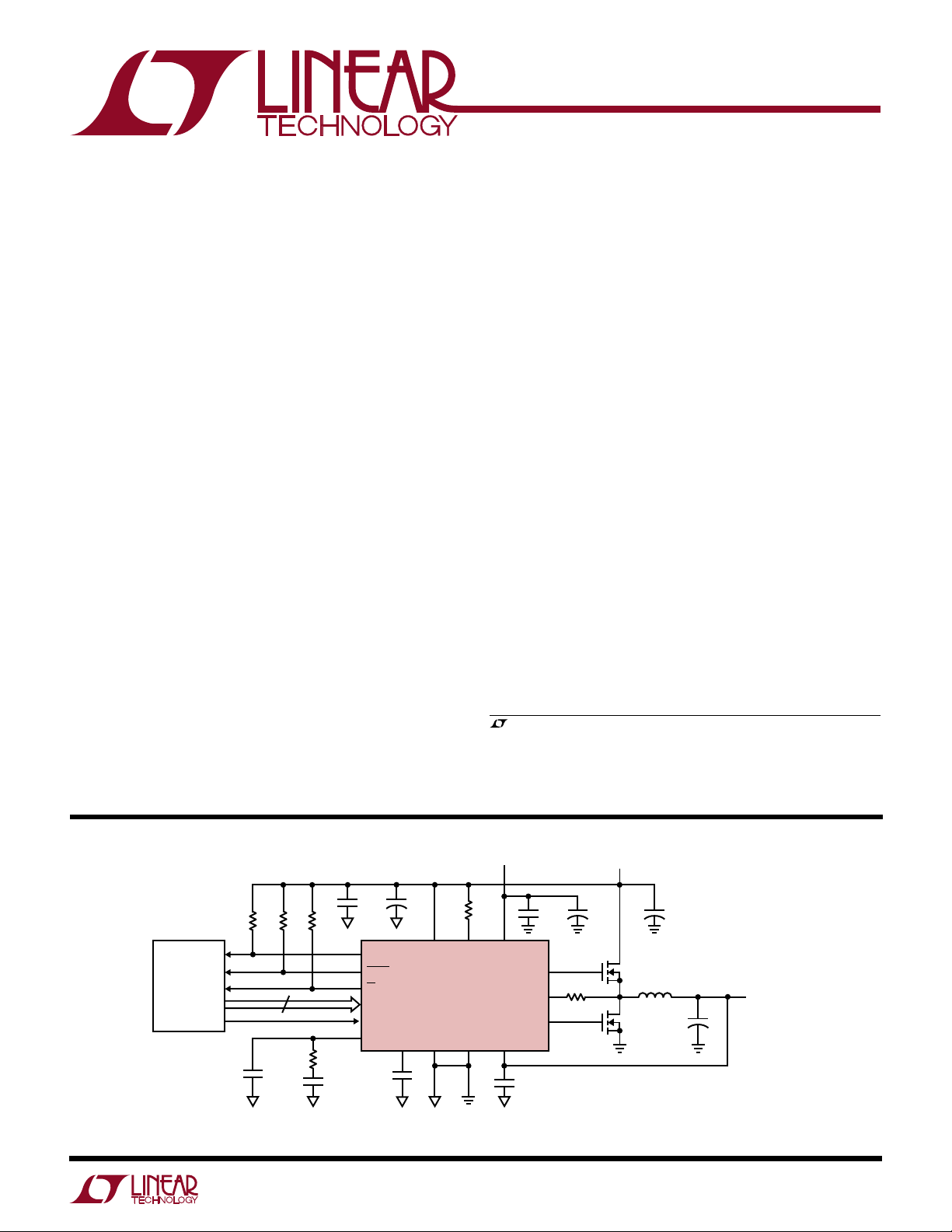
TYPICAL APPLICATION
5.6k
5.6k
PENTIUM® II
SYSTEM
C1
150pF
5
5.6k
R
8.2k
U
C
CC
0.01µF
+
0.1µF
10µF CIN**
PWRGD
FAULT
OT
VID0 TO VID4
OUTEN
COMP
C
SS
0.1µF
V
SS SGND GND SENSE
CC
LTC1553
PV
CC
12V
2.7k
I
MAX
0.1µF
PV
CC
G1
I
FB
G2
0.1µF
Figure 1. 5V to 1.8V-3.5V Supply Application
V
IN
5V
+
10µF
Q1*
20Ω
Q2*
*SILICONIX SUD50N03-10
**SANYO 10MV1200GX
†
COILTRONICS CTX02-13198 OR
PANASONIC 12TS-2R5SP
††
AVX TPSE337M006R0100
+
L
2µH
18A
O†
1200µF
× 4
C
OUT
330µF
× 7
V
OUT
1.8V TO
††
+
3.5V
14A
1553 F01
1
Page 2
LTC1553
WW
W
U
ABSOLUTE MAXIMUM RATINGS
(Note 1)
Supply Voltage
VCC........................................................................ 9V
PVCC................................................................... 20V
Input Voltage
IFB (Note 2)............................................ PVCC + 0.3V
I
...................................................... –0.3V to 13V
MAX
All Other Inputs ......................... –0.3V to VCC + 0.3V
Digital Output Voltage............................... – 0.3V to 13V
IFB Input Current (Notes 2, 3) .......................... – 100mA
Operating Temperature Range ..................... 0°C to 70°C
Storage Temperature Range ................. –65°C to 150°C
Lead Temperature (Soldering, 10 sec.)................. 300°C
ELECTRICAL CHARACTERISTICS
VCC = 5V, PVCC = 12V, TA = 25°C, unless otherwise noted. (Note 3)
U
W
PACKAGE/ORDER INFORMATION
TOP VIEW
1
G2
2
PV
CC
3
GND
4
SGND
5
V
CC
6
SENSE
7
I
MAX
8
I
FB
9
SS
10
COMP
G PACKAGE
20-LEAD PLASTIC SSOP
T
= 125°C, θJA = 100°C/ W (G)
JMAX
= 125°C, θJA = 100°C/ W (SW)
T
JMAX
20-LEAD PLASTIC SO
G1
20
OUTEN
19
VID0
18
VID1
17
VID2
16
VID3
15
VID4
14
PWRGD
13
FAULT
12
OT
11
SW PACKAGE
Consult factory for Industrial and Military grade parts.
ORDER PART
NUMBER
LTC1553CG
LTC1553CSW
U
SYMBOL PARAMETER CONDITIONS MIN TYP MAX UNITS
V
PV
V
V
CC
CC
FB
OUT
Supply Voltage ● 4.5 8 V
Supply Voltage for G1, G2 ● 18 V
Internal Feedback Voltage (Note 4) 1.265 V
1.8V Initial Output Voltage With Respect to Rated Output Voltage (Figure 2) – 27 (–1.5%) 27 (+1.5%) mV
2.8V Initial Output Voltage – 42 (–1.5%) 42 (+ 1.5%) mV
3.5V Initial Output Voltage – 52 (–1.5%) 52 (+1.5%) mV
1.8V Initial Output Voltage
2.8V Initial Output Voltage
3.5V Initial Output Voltage
∆V
OUT
Output Load Regulation I
Output Line Regulation V
V
PWRGD
Positive Power Good Trip Point % Above Output Voltage (Figure 2) ● 57 %
Negative Power Good Trip Point % Below Output Voltage (Figure 2)
V
FAULT
I
CC
FAULT Trip Point % Above Output Voltage (Figure 2) ● 12 15 20 %
Operating Supply Current OUTEN = VCC = 5V (Note 5) (Figure 3) ● 800 1200 µA
Shutdown Supply Current OUTEN = 0, VID0 to VID4 Floating (Figure 3)
I
PVCC
f
OSC
V
V
G
g
BW
SAWL
SAWH
ERR
mERR
ERR
Supply Current PVCC = 12V, OUTEN = VCC (Note 6) (Figure 3) 15 mA
Internal Oscillator Frequency (Figure 4) ● 250 300 350 kHz
V
at Minimum Duty Cycle (Note 4) 1.8 V
COMP
V
at Maximum Duty Cycle (Note 4) 2.8 V
COMP
Error Amplifier Open-Loop DC Gain (Note 7) ● 40 53 dB
Error Amplifier Transconductance (Note 7) ● 0.9 1.6 2.3 millimho
Error Amplifier –3dB Bandwidth COMP = Open (Note 4) 400 kHz
= 0 to 14A (Note 4) (Figure 2) –5 mV
OUT
= 4.75V to 5.25V, I
IN
= 12V, OUTEN = 0, VID0 to VID4 Floating 1 µA
PV
CC
= 0 (Note 4)(Figure 2) ±1mV
OUT
● – 36 (–2%) 36 (+2%) mV
● – 56 (–2%) 56 (+2%) mV
● – 70 (–2%) 70 (+2%) mV
● –7 –5 %
● 130 250 µA
2
Page 3
LTC1553
ELECTRICAL CHARACTERISTICS
VCC = 5V, PVCC = 12V, TA = 25°C, unless otherwise noted. (Note 3)
SYMBOL PARAMETER CONDITIONS MIN TYP MAX UNITS
I
IMAX
I
SS
I
SSIL
I
SSHIL
I
Sink Current V
MAX
Soft Start Source Current VSS = 0V, V
Maximum Soft Start Sink Current V
IMAX
SENSE
= V
= V
CC
IMAX
OUT
Under Current Limit (Notes 8, 9), V
Soft Start Sink Current Under Hard V
SENSE
= 0V, V
= 0V, V
, V
IMAX
= V
SS
IMAX
IFB
= VCC, V
CC
= VCC, V
● 150 180 220 µA
= V
CC
= 0V ● 30 60 150 µA
IFB
= 0V ● 20 45 mA
IFB
● –13 –10 –7 µA
Current Limit
t
SSHIL
t
PWRGD
t
PWRBAD
t
FAULT
t
OT
V
OT
V
OTDD
V
SHDN
tr, t
f
t
NOL
DC
MAX
V
IH
V
IL
R
IN
Hard Current Limit Hold Time V
Power Good Response Time↑ V
Power Good Response Time↓ V
FAULT Response Time V
= 0V, V
SENSE
SENSE
SENSE
SENSE
IMAX
↑ from 0V to Rated V
↓ from Rated V
↑ from Rated V
= 4V, V
↓ from 5V (Note 4) 500 µs
IFB
OUT
to 0V ● 200 500 1000 µs
OUT
to V
OUT
CC
● 0.5 1 2 ms
● 200 500 1000 µs
OT Response Time OUTEN↓, VID0 to VID4 = 0 (Note 10) (Figure 3) ● 15 40 60 µs
Over-Temperature Trip Point OUTEN↓, VID0 to VID4 = 0 (Note 10) (Figure 3) ● 1.9 2 2.12 V
Over-Temperature Driver Disable OUTEN↓, VID0 to VID4 = 0 (Note 10) (Figure 3) ● 1.6 1.7 1.8 V
Shutdown OUTEN↓, VID0 to VID4 = 0 (Note 10) (Figure 3) ● 0.8 V
Driver Rise and Fall Time (Figure 4) ● 90 150 ns
Driver Nonoverlap Time (Figure 4) ● 30 100 ns
Maximum G1 Duty Cycle (Figure 4) ● 77 84 88 %
VID0 to VID4 Input High Voltage ● 2V
VID0 to VID4 Input Low Voltage ● 0.8 V
VID0 to VID4 Internal Pull-Up ● 10 20 kΩ
Resistance
I
SINK
Digital Output Sink Current ● 10 mA
The ● denotes specifications which apply over the full operating
temperature range.
Note 1: Absolute Maximum Ratings are those values beyond which the life
of a device may be impaired.
Note 2: When I
is taken below GND, it will be clamped by an internal
FB
diode. This pin can handle input currents greater than 100mA below GND
without latchup. In the positive direction, it is not clamped to V
or PVCC.
CC
Note 3: All currents into device pins are positive; all currents out of the
device pins are negative. All voltages are referenced to ground unless
otherwise specified.
Note 4: This parameter is guaranteed by correlation and is not tested
directly.
Note 5: The LTC1553 goes into the shutdown mode if VID0 to VID4 are
floating. Due to the internal pull-up resistors, there will be an additional
0.25mA/pin if any of the VID0 to VID4 pins are pulled low.
Note 6: Supply current in normal operation is dominated by the current
needed to charge and discharge the external FET gates. This will vary with
the LTC1553 operating frequency, supply voltage and the external FETs
used.
Note 7: The open-loop DC gain and transconductance from the SENSE pin to
COMP pin will be (G
)(1.265/3.3) and (g
ERR
)(1.265/3.3) respectively.
mERR
Note 8: The current limiting amplifier can sink but cannot source current.
Under normal (not current limited) operation, the output current will be zero.
Note 9: Under typical soft current limit, the net soft start discharge current
will be 60µA (I
) + [–10µA(ISS)] = 50µ A. The soft start sink-to-source
SSIL
current ratio is designed to be 6:1.
Note 10: When VID0 to VID4 are all HIGH, the LTC1553 will be forced to
shut down internally. The OUTEN trip voltages are guaranteed by design for
all other input codes.
3
Page 4
LTC1553
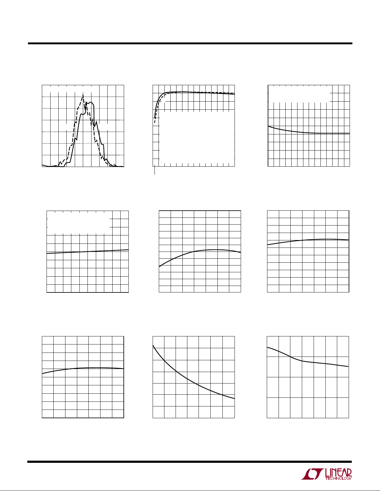
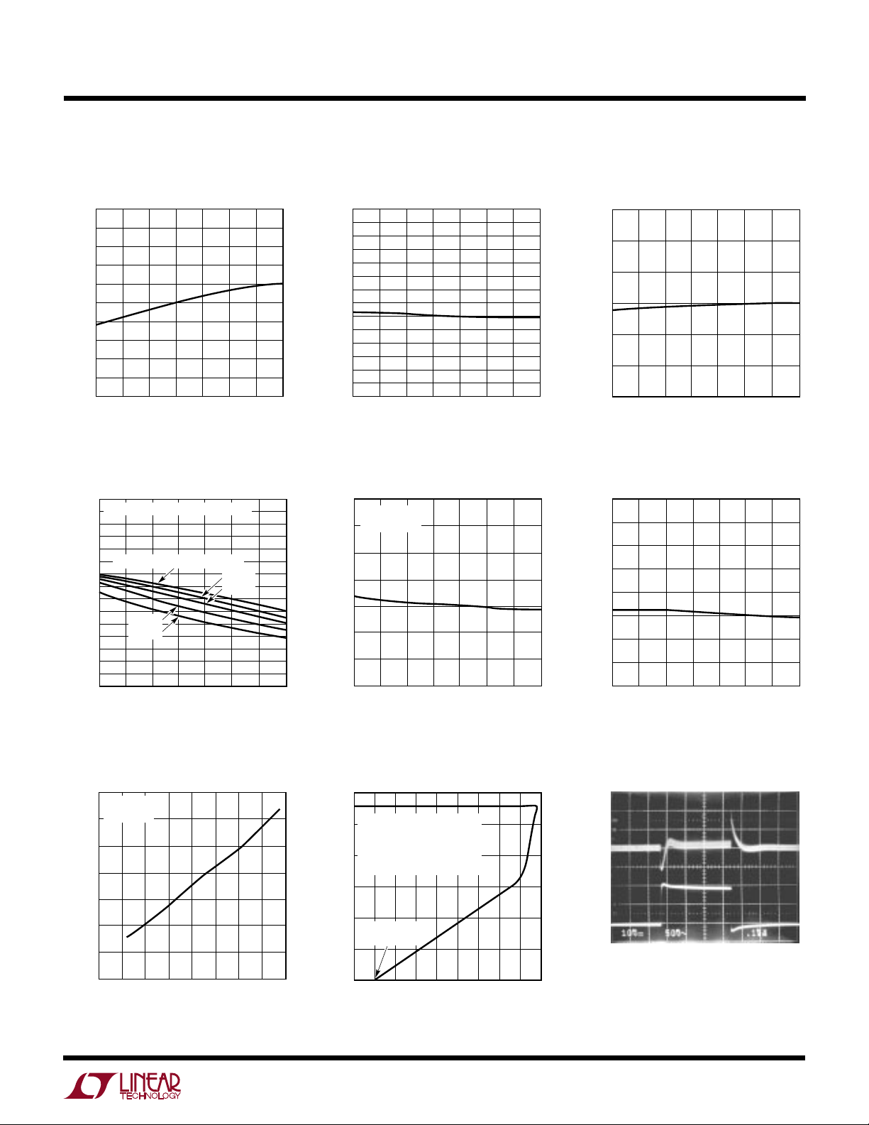
OUTPUT CURRENT (A)
0
OUTPUT VOLTAGE (V)
2.825
4
1533 G03
2.820
2.815
2.810
2.805
2.800
2.795
2.790
2.785
2.780
2.775
123
5
67891011121314
REFER TO TYPICAL APPLICATION
CIRCUIT FIGURE 1
V
IN
= 5V, PVCC = 12V, TA = 25°C
TEMPERATURE (°C)
–50
OVER-TEMPERATURE TRIP POINT (V)
1.96
2.08
2.10
2.12
0
50
75
1553 G06
1.92
2.04
2.00
1.94
2.06
1.90
2.02
1.98
–25
25
100
125
UW
TYPICAL PERFORMANCE CHARACTERISTICS
Typical 2.8V V
140
TOTAL SAMPLE SIZE = 1500
120
100
80
60
NUMBER OF UNITS
40
20
0
2.775
2.785
25°C 100°C
OUTPUT VOLTAGE (V)
OUT
2.795
Distribution
2.805 2.815
1553 G01
2.825
Efficiency vs Load Current
100
90
A
B
80
70
REFER TO TYPICAL APPLICATION
60
CIRCUIT FIGURE 1
= 5V, PVCC = 12V, V
V
50
IN
= 330µF ×7, LO = 2µH
C
OUT
40
EFFICIENCY (%)
A: Q1 = 1 × SUD50N03-10
Q2 = 1 × SUD50N03-10
30
B: Q1 = 2 × SUD50N03-10
20
Q2 = 1 × SUD50N03-10
NO FAN
10
Q1 IS MOUNTED ON 1IN
0
0
2
0.3
4
LOAD CURRENT (A)
Line Regulation Output Temperature Drift
2.825
REFER TO TYPICAL APPLICATION
2.820
CIRCUIT FIGURE 1
OUTPUT = NO LOAD
2.815
2.810
2.805
2.800
2.795
2.790
OUTPUT VOLTAGE (V)
2.785
2.780
2.775
4.75
T
A
= 25°C
4.85
5.05
4.95
INPUT VOLTAGE (V)
5.15
5.25
1553 G04
2.860
2.850
2.840
2.830
2.820
2.810
2.800
2.790
2.780
OUTPUT VOLTAGE (V)
2.770
2.660
2.750
2.740
–50
–25
0
TEMPERATURE (°C)
= 2.8V,
OUT
2
COPPER AREA
6 8 10 12 14
1533 G02
50
25
75
100
1553 G05
Load Regulation
Over-Temperature Trip Point
vs Temperature
125
Over-Temperature Driver Disable
vs Temperature
1.80
1.78
1.76
1.74
1.72
1.70
1.68
1.66
1.64
1.62
OVER-TEMPERATURE DRIVER DISABLE (V)
1.60
–50
4
0
–25
TEMPERATURE (°C)
Error Amplifier Transconductance
vs Temperature
2.3
2.1
1.9
1.7
1.5
1.3
1.1
50
25
75
100
125
1553 G07
0.9
ERROR AMPLIFIER TRANSCONDUCTANCE (millimho)
–50
–25 0
TEMPERATURE (°C)
50 100 125
25 75
1553 G08
Error Amplifier Open-Loop
DC Gain vs Temperature
60
55
50
45
ERROR AMPLIFIER OPEN-LOOP DC GAIN (dB)
40
–50
–25 0 25 50
TEMPERATURE (°C)
75 100 125
1553 G09
Page 5
UW
TYPICAL PERFORMANCE CHARACTERISTICS
LTC1553
Oscillator Frequency
vs Temperature
350
340
330
320
310
300
290
280
270
OSCILLATOR FREQUENCY (kHz)
260
250
–50
–25
25
0
TEMPERATURE (°C)
Maximum G1 Duty Cycle
vs Temperature
92
OSCILLATOR FREQUENCY = 300kHz
90
88
G1, G2 CAPACITANCE = 1100pF
86
84
–50
5500pF
7700pF
–25 0
25 75
TEMPERATURE (°C)
82
80
MAXIMUM G1 DUTY CYCLE (%)
78
50
75
2200pF
3300pF
50 100 125
100
125
1553 G10
1553 G13
I
Sink Current
MAX
vs Temperature
220
210
200
190
180
SINK CURRENT (µA)
170
MAX
I
160
150
–50
0
–25
TEMPERATURE (°C)
25
VCC Operating Supply Current
vs Temperature
1.2
VCC = 5V
= 300kHz
f
OSC
1.1
1.0
0.9
0.8
0.7
OPERATING SUPPLY CURRENT (mA)
0.6
CC
V
0.5
–50
–25 0
25 75
TEMPERATURE (°C)
75
50 125
50 100 125
100
1553 G11
1553 G14
Soft Start Source Current
vs Temperature
–7
–8
–9
–10
–11
–12
SOFT START SOURCE CURRENT (µA)
–13
–50
–25 0
TEMPERATURE (°C)
50 100 125
25 75
VCC Shutdown Supply Current
vs Temperature
250
225
200
175
150
125
100
SHUTDOWN SUPPLY CURRENT (mA)
75
CC
V
50
–25 0 50
–50
25
TEMPERATURE (°C)
1553 G12
75 100 125
1553 G15
PVCC Supply Current
vs Gate Capacitance
70
PVCC = 12V
= 25°C
T
A
60
50
40
30
SUPPLY CURRENT (mA)
20
CC
PV
10
0
2000 4000 8000
0
GATE CAPACITANCE (pF)
6000
1553 G16
Output Over Current Protection
3.0
Q1 CASE = 90°C, V
2.5
Q1 = 2 × MTD20N03HDL
Q2 = 1 × MTD20N03HDL
2.0
1.5
1.0
OUTPUT VOLTAGE (V)
0.5
= 2.7k, R
R
IMAX
SS CAP = 0.01µF
SHORT-CIRCUIT
CURRENT
0
26
0
4
OUTPUT CURRENT (A)
= 2.8V
OUT
= 20Ω,
IFB
10 18
8
Transient Response
50mV/DIV
5A/DIV
100µs/DIV
14
16
12
1553 G17
1553 G18
5
Page 6

LTC1553
PIN FUNCTIONS
UUU
G2 (Pin 1): Gate Drive for the Lower N-Channel MOSFET,
Q2. This output will swing from PVCC to GND. It will always
be low when G1 is high or when the output is disabled. To
prevent undershoot during a soft start cycle, G2 is held low
until G1 first goes high.
PVCC (Pin 2): Power Supply for G1 and G2. PVCC must be
connected to a potential of at least VIN + V
VIN = 5V, PVCC can be generated using a simple charge
pump connected to the switching node between Q1 and
Q2 (see Figure 7), or it can be connected to an auxiliary 12V
supply if one exists. For applications where VIN = 12V,
PVCC can be generated using a 17V charge pump (see
Figure 9).
GND (Pin 3): Power Ground. GND should be connected to
a low impedance ground plane in close proximity to the
source of Q2.
SGND (Pin 4): Signal Ground. SGND is connected to the
low power internal circuitry and should be connected to
the negative terminal of the output capacitor where it
returns to the ground plane. GND and SGND should be
shorted right at the LTC1553.
VCC (Pin 5): Power Supply. Power for the internal low
power circuity. VCC should be wired separately from the
drain of Q1 if they share the same supply. A 10µ F bypass
capacitor is recommended from this pin to SGND.
SENSE (Pin 6): Output Voltage Pin. Connect to the positive
terminal of the output capacitor. There is an internal 120k
resistor connected from this pin to SGND. SENSE is a very
sensitive pin; for optimum performance, connect an external 0.1µ F capacitor from this pin to SGND. By connecting
a small external resistor between the output capacitor and
the SENSE pin, the initial output voltage can be raised
slightly. Since the internal divider has a nominal impedance of 120kΩ, a 1200Ω series resistor will raise the
nominal output voltage by 1%. If an external resistor is
used, the value of the 0.1µF capacitor on the SENSE pin
must be greatly reduced or loop phase margin will suffer.
Set a time constant for the RC combination of approximately 0.1µ s. So, for example, with a 1200Ω resistor, set
C = 83pF. Use a standard 100pF capacitor.
GS(ON)Q1
. If
I
(Pin 7): Current Limit Threshold. Current limit is set
MAX
by the voltage drop across an external resistor connected
between the drain of Q1 and I
pull-down at I
IFB (Pin 8): Current Limit Sense Pin. Connect to the
switching node between the source of Q1 and the drain of
Q2. If IFB drops below I
will go into current limit. The current limit circuit can be
disabled by floating I
an external 10k resistor. For VIN = 12V, a 15V Zener diode
from IFB to GND is recommended to prevent the voltage
spike at IFB from exceeding the maximum voltage rating.
SS (Pin 9): Soft Start. Connect to an external capacitor to
implement a soft start function. During moderate overload
conditions, the soft start capacitor will be discharged
slowly in order to reduce the duty cycle. In hard current
limit, the soft start capacitor will be forced low immediately and the LTC1553 will rerun a complete soft start
cycle. CSS must be selected such that during power-up the
current through Q1 will not exceed the current limit value.
COMP (Pin 10): External Compensation. The COMP pin is
connected directly to the output of the error amplifier and
the input of the PWM comparator. An RC+ C network is
used at this node to compensate the feedback loop to
provide optimum transient response.
OT (Pin 11): Over-Temperature Fault. OT is an open-drain
output and will be pulled low if OUTEN is less than 2V. If
OUTEN = 0, OT pulls low.
FAULT (Pin 12): Overvoltage Fault. FAULT is an opendrain output. If V
output voltage, FAULT will go low and G1 and G2 will be
disabled. Once triggered, the LTC1553 will remain in this
state until the power supply is recycled or the OUTEN pin
is toggled. If OUTEN = 0, FAULT floats or is pulled high by
an external resistor.
PWRGD (Pin 13): Power Good. This is an open-drain
signal to indicate validity of output voltage. A high indicates that the output has settled to within ±5% of the rated
output for more than 1ms. PWRGD will go low if the output
is out of regulation for more than 500µs. If OUTEN = 0,
PWRGD pulls low.
MAX
.
MAX
and shorting IFB to VCC through
MAX
reaches 15% above the nominal
OUT
. There is a 180µ A internal
MAX
when G1 is on, the LTC1553
6
Page 7
UUU
PIN FUNCTIONS
LTC1553
VID0, VID1, VID2, VID3, VID4 (Pins 18, 17, 16, 15, 14):
Digital Voltage Select. TTL inputs used to set the regulated
output voltage required by the processor (Table 3). There
is an internal 20kΩ pull-up at each pin. When all five VID
n
pins are high or floating, the chip will shut down.
OUTEN (Pin 19): Output Enable. TTL input which enables
the output voltage. The external MOSFET temperature can
be monitored with an external thermistor as shown in
Figure 13. When the OUTEN input voltage drops below 2V,
W
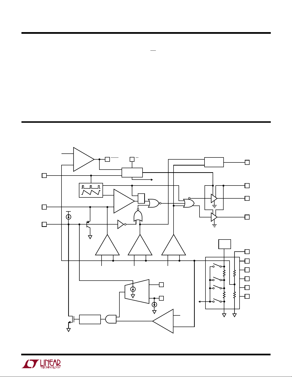
BLOCK DIAGRAM
OUTEN
COMP
19
10
115% V
REF
+
FC
FAULT
12
OT
11
–
LOGIC
–
PWM
+
R
S
OT trips. As OUTEN drops below 1.7V, the drivers are
internally disabled to prevent the MOSFETs from heating
further. If OUTEN is less than 1.2V for longer than 30µs,
the LTC1553 will enter shutdown mode. The internal
oscillator can be synchronized to a faster external clock by
applying the external clocking signal to the OUTEN pin.
G1 (Pin 20): Gate Drive for the Upper N-Channel MOSFET,
Q1. This output will swing from PVCC to GND. It will always
be low when G2 is high or the output is disabled.
DISDR
SYSTEM
POWER
DOWN
DELAY
13
2
20
PWRGD
PV
CC
G1
I
SS
SS
9
Q
SS
ERR
+
–
V
REF
HCL MONOMHCL
MIN
+
–
V
– 5% V
REF
–
CC
+
I
MAX
8
7
REF
LVC
I
I
FB
MAX
+ 5%
MAX
–+
+
0.5V
0.7V
REF
REF
FB
V
REF
/
BG
DAC
–
1
6
18
17
16
15
14
G2
SENSE
VID0
VID1
VID2
VID3
VID4
1553 BD
7
Page 8
LTC1553
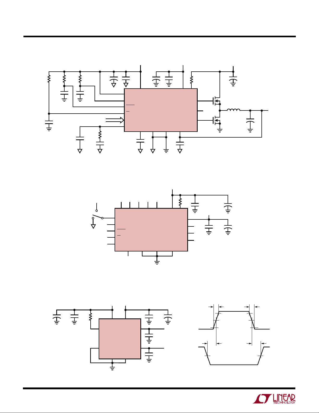
TEST CIRCUITS
3k3k
0.1µF
PV
12V
CC
10k
V
IN
5V
CIN**
+
1200µF
× 4
V
CC
5V
3k
10µF
0.1µF
++
10µF
100pF
100pF
100pF
VID0 TO VID4
C1
150pF
V
CC
R
C
8.2k
CC
0.01µF
VID0 VID1 VID2 VID3 VID4
VID0 VID1 VID2 VID3 VID4
OUTEN
PWRGD
NC
FAULT
NC
OT
NC
COMP
NC
V
CC
OUTEN
PWRGD
FAULT
OT
VID0 TO VID4
COMP
SS SGND GND SENSE
0.1µF
LTC1553
Figure 2
V
CC
V
CC
LTC1553
SS SGND GND SENSE
PV
I
PV
I
MAX
I
FB
CC
G1
NC
I
MAX
G2
0.1µF
10k
FB
CC
G1
NC
NC
G2
NC
*SILICONIX SUD50N03-10
**SANYO 10MV1200GX
PANASONIC 12TS-2R5SP
††
0.1µF
PV
CC
0.1µF
L
O†
Q1*
2µH
15A
††
C
+
Q2*
†
COILTRONICS CTX02-13198 OR
AVX TPSE337M006R0100
OUT
330µF
× 7
+
10µF
+
10µF
V
OUT
1553 F02
8
NC
1553 F03
Figure 3
V
PV
CC
CC
5V
12V
+
10µF
0.1µF
10k
I
FB
SENSE
SGND GND
V
CC
LTC1553
PV
CC
G1
G2
0.1µF
5000pF
5000pF
+
10µF
G1 RISE/FALL
G2 RISE/FALL
t
r
90%
50%
10%
t
NOL
50% 50%
90%
50%
10%
t
f
t
NOL
1553 F04
Figure 4
Page 9

U U
FU CTIO TABLES
LTC1553
Table 1. OT Logic
OUTEN (V) OT*
< 2 0
> 2 1
Table 2. PWRGD and FAULT Logic
INPUT OUTPUT*
OUTEN V
0 X 010
1 < 95% 1 1 0
1 > 95% 1 1 1
1 >105% 1 1 0
1 > 115% 1 0 0
** OT FAULT PWRGD
SENSE
< 105%
Table 3. Rated Output Voltage
INPUT PIN
V
V
ID4
01111Disabled† (1.30)
01110Disabled† (1.35)
01101Disabled† (1.40)
01100Disabled† (1.45)
01011Disabled† (1.50)
01010Disabled† (1.55)
01001Disabled† (1.60)
01000Disabled† (1.65)
00111Disabled† (1.70)
00110Disabled† (1.75)
ID3
V
ID2
V
ID1
V
ID0
RATED OUTPUT
VOLTAGE (V)
Table 3. Rated Output Voltage (cont)
INPUT PIN
V
* With external pull-up resistor
** With respect to the output voltage selected in Table 3 as required by
†
X Don’t care
V
ID4
00101 1.80
00100 1.85
00011 1.90
00010 1.95
00001 2.00
00000 2.05
11111 SHDN
11110 2.1
11101 2.2
11100 2.3
11011 2.4
11010 2.5
11001 2.6
11000 2.7
10111 2.8
10110 2.9
10101 3.0
10100 3.1
10011 3.2
10010 3.3
10001 3.4
10000 3.5
Intel Specification VRM 8.2
These code selections are disabled in LTC1553
ID3
V
ID2
V
ID1
V
ID0
RATED OUTPUT
VOLTAGE (V)
9
Page 10

LTC1553
U
WUU
APPLICATIONS INFORMATION
OVERVIEW
The LTC1553 is a voltage feedback, synchronous switching regulator controller (see Block Diagram) designed for
use in high power, low voltage step-down (buck) converters. It is designed to satisfy the requirements of the Intel
Pentium II power supply specification. It includes an
on-chip DAC to control the output voltage, a PWM generator, a precision reference trimmed to ±1%, two high power
MOSFET gate drivers and all the necessary feedback and
control circuitry to form a complete switching regulator
circuit.
The LTC1553 includes a current limit sensing circuit that
uses the upper external power MOSFET as a current
sensing element, eliminating the need for an external
sense resistor. Once the current comparator, CC, detects
an overcurrent condition, the duty cycle is reduced by
discharging the soft start capacitor through a voltagecontrolled current source. Under severe overloads or
output short circuit conditions, the chip will be repeatedly
forced into soft start until the short is removed, preventing
the external components from being damaged. Under
output overvoltage conditions, the MOSFET drivers will be
disabled permanently until the chip power supply is
recycled or the OUTEN pin is toggled.
Output regulation can be monitored with the PWRGD pin
which in turn monitors the internal MIN and MAX comparators. If the output is ±5% beyond the selected value
for more than 500µs, the PWRGD output will be pulled
low. Once the output has settled within ±5% of the
selected value for more than 1ms, PWRGD will return
high.
THEORY OF OPERATION
Primary Feedback Loop
The regulator output voltage at the SENSE pin is divided
down internally by a resistor divider with a total resistance
of approximately 120kΩ. This divided down voltage is
subtracted from a reference voltage supplied by the DAC
output. The resulting error voltage is amplified by the error
amplifier and the output is compared to the oscillator ramp
waveform by the PWM comparator. This PWM signal
controls the external MOSFETs through G1 and G2. The
resulting chopped waveform is filtered by LO and C
closing the loop. Loop frequency compensation is achieved
with an external RC + C network at the COMP pin, which is
connected to the output node of the transconductance
amplifier.
OUT
OUTEN can optionally be connected to an external negative temperature coefficient (NTC) thermistor placed near
the external MOSFETs or the microprocessor. Three threshold levels are provided internally. When OUTEN drops to
2V, OT will trip, issuing a warning to the external CPU. If
the temperature continues to rise and the OUTEN input
drops to 1.7V, the G1 and G2 pins will be forced low. If
OUTEN is pulled below 1.2V, the LTC1553 will go into
shutdown mode, cutting the supply current to a minimum.
If thermal shutdown is not required, OUTEN can be connected to a conventional TTL enable signal. The freerunning 300kHz PWM frequency can be synchronized to
a faster external clock connected to OUTEN. Adjusting the
oscillator frequency can add flexibility in the external
component selection. See the Clock Synchronization
section.
MIN, MAX Feedback Loops
Two additional comparators in the feedback loop provide
high speed fault correction in situations where the ERR
amplifier may not respond quickly enough. MIN compares
the feedback signal FB to a voltage 60mV (5%) below the
internal reference. If FB is lower than the threshold of this
comparator, the MIN comparator overrides the ERR
amplifier and forces the loop to full duty cycle which is set
by the internal oscillator typically to 84%. Similarly, the
MAX comparator forces the output to 0% duty cycle if FB
is more than 5% above the internal reference. To prevent
these two comparators from triggering due to noise, the
MIN and MAX comparators’ response times are deliberately controlled so that they take two to three microseconds to respond. These two comparators help prevent
extreme output perturbations with fast output transients,
while allowing the main feedback loop to be optimally
compensated for stability.
10
Page 11

LTC1553
II
I
LMAX LOAD
RIPPLE
=+
2
Q1
180µA
G1
Q2
C
IN
L
O
V
OUT
1553 F05
C
OUT
R
IMAX
V
IN
–
+
CC
G2
20Ω
LTC1553
I
MAX
I
FB
8
7
+
+
APPLICATIONS INFORMATION
Soft Start and Current Limit
The LTC1553 includes a soft start circuit which is used for
initial start-up and during current limit operation. The SS
pin requires an external capacitor to GND with the value
determined by the required soft start time. An internal
10µA current source is included to charge the external SS
capacitor. During start-up, the COMP pin is clamped to a
diode drop above the voltage at the SS pin. This prevents
the error amplifier, ERR, from forcing the loop to maximum duty cycle. The LTC1553 will begin to operate at low
duty cycle as the SS pin rises above about 1.2V (V
1.8V). As SS continues to rise, QSS turns off and the error
amplifier begins to regulate the output. The MIN comparator is disabled when soft start is active to prevent it from
overriding the soft start function.
The LTC1553 includes yet another feedback loop to control operation in current limit. Just before every falling
edge of G1, the current comparator, CC, samples and
holds the voltage drop measured across the external
MOSFET, Q1, at the IFB pin. Note that when VIN = 12V, the
IFB pin requires an external Zener to GND to prevent
voltage transients at the switching node between Q1 and
Q2 from damaging internal structures. CC compares the
voltage at IFB to the voltage at the I
current rises, the measured voltage across Q1 increases
due to the drop across the R
at IFB drops below I
has exceeded the maximum level, CC starts to pull current
out of the external soft start capacitor, cutting the duty
cycle and controlling the output current level. The CC
comparator pulls current out of the SS pin in proportion to
the voltage difference between IFB and I
overload conditions, the SS pin will fall gradually, creating
a time delay before current limit takes effect. Very short,
mild overloads may not affect the output voltage at all.
More significant overload conditions will allow the SS pin
to reach a steady state, and the output will remain at a
reduced voltage until the overload is removed. Serious
overloads will generate a large overdrive at CC, allowing it
to pull SS down quickly and preventing damage to the
output components.
U
DS(ON)
, indicating that Q1’s drain current
MAX
WUU
pin. As the peak
MAX
of Q1. When the voltage
. Under minor
MAX
COMP
By using the R
of Q1 to measure the output current,
DS(ON)
the current limiting circuit eliminates an expensive discrete sense resistor that would otherwise be required. This
helps minimize the number of components in the high
current path. Due to switching noise and variation of
R
, the actual current limit trip point is not highly
DS(ON)
accurate. The current limiting circuitry is primarily meant
to prevent damage to the power supply circuitry during
fault conditions. The exact current level where the limiting
circuit begins to take effect will vary from unit to unit as the
≈
R
DS(ON)
of Q1 varies.
For a given current limit level, the external resistor from
I
to VIN can be determined by:
MAX
IR
R
IMAX
()( )
LMAX DS ON Q
=
()1
I
IMAX
where,
I
= Maximum load current
LOAD
I
f
= Inductor ripple current
RIPPLE
VV V
−
()()
IN OUT OUT
=
= LTC1553 oscillator frequency = 300kHz
OSC
fLV
()()()
OSC O IN
LO = Inductor value
R
DS(ON)Q1
I
IMAX
= Hot on-resistance of Q1 at I
= Internal 180µA sink current at I
Figure 5. Current Limit Setting
LMAX
MAX
11
Page 12

LTC1553
U
WUU
APPLICATIONS INFORMATION
Table 4. Recommended Minimum R
MAXIMUM OPERATING SUD50N03-10 MTD20N03HDL
LOAD CURRENT (A) SUD50N03-10 (TWO IN PARALLEL) MTD20N03HDL (TWO IN PARALLEL)
12 2.4 1.2 4.3 2.2
14 2.7 1.3 5.1 2.7
16 3.0 1.5 6.2 3.0
18 3.6 1.8 6.8 3.3
20 3.9 2.0 7.5 3.6
OUTEN and Thermistor Input
The LTC1553 includes a low power shutdown mode,
controlled by the logic at the OUTEN pin. A high at OUTEN
allows the part to operate normally. A low level at OUTEN
stops all internal switching, pulls COMP and SS to ground
internally and turns Q1 and Q2 off. OT and PWRGD are
pulled low, and FAULT is left floating. In shutdown, the
LTC1553 quiescent current will drop to about 130µ A. The
remaining current is used to keep the thermistor sensing
circuit at OUTEN alive. Note that the leakage current of
the external MOSFETs may add to the total shutdown
current consumed by the circuit, especially at elevated
temperature.
OUTEN is designed with multiple thresholds to allow it to
also be utilized for over-temperature protection. The power
MOSFET operating temperature can be monitored with an
external negative temperature coefficient (NTC) thermistor
mounted next to the external MOSFET which is expected
to run the hottest–– often the high-side device, Q1. Electrically, the thermistor should form a voltage divider with
another resistor, R1, connected to VCC. Their midpoint
should be connected to OUTEN (see Figure 6). As the
temperature increases, the OUTEN pin voltage is reduced.
Under normal operating conditions, the OUTEN pin should
stay above 2V. All circuits will function normally, and the
OT pin will remain in a high state. If the temperature gets
abnormally high, the OUTEN pin voltage will eventually
drop below 2V. OT will switch to a logic low, providing an
over-temperature warning to the system. As OUTEN drops
below 1.7V, the LTC1553 disables both FET drivers. If
Resistor (kΩ) vs Maximum Operating Load Current and External MOSFET Q1
IMAX
V
CC
5.6k
PENTIUM II
SYSTEM
NTC THERMISTOR
MOUNT IN CLOSE
THERMAL PROXIMITY
TO Q1
Figure 6. OUTEN Pin as a Thermistor Input
OT
V
CC
R1
R2
OUTEN
G1
LTC1553
G2
OUTEN is less than 1.2V, the LTC1553 will enter shutdown
mode. To activate any of these three modes, the OUTEN
voltage must drop below the respective threshold for
longer than 30µs.
Clock Synchronization
The internal oscillator can be synchronized to an external
clock by applying the external clocking signal to the
OUTEN pin. The synchronizing range extends from the
initial operating frequency up to 500kHz. If the external
frequency is much higher than the natural free-running
frequency, the peak-to-peak sawtooth amplitude within
the LTC1553 will decrease. Since the loop gain is inversely
proportional to the amplitude of the sawtooth, the compensation network may need to be adjusted slightly. Note
that the temperature sensing circuitry does not operate
when external synchronization is used.
V
IN
Q1
L
O
Q2
V
OUT
+
C
OUT
1553 F06
12
Page 13

LTC1553
Q1
G1
Q2
0.1µF
L
O
V
OUT
1553 F07
C
OUT
C
IN
V
IN
PV
CC
1N5248B
18V
1N5817
OPTIONAL FOR V
IN
> 5V
G2
LTC1553
20
1
2
+
+
Q1
Q2
0.1µF
0.1µF
10µF
L
O
V
OUT
1553 F08
C
OUT
C
IN
V
IN
1N5248B
18V
1N5817
LTC1553
1N5817 1N5817
+
G1
PV
CC
G2
20
1
2
+
+
U
WUU
APPLICATIONS INFORMATION
MOSFET Gate Drive
Power for the internal MOSFET drivers is supplied by
PVCC. This supply must be above the input supply voltage
by at least one power MOSFET V
tion. This higher voltage can be supplied with a separate
supply, or it can be generated using a simple charge pump
as shown in Figure 7. The 84% typical maximum duty
cycle ensures sufficient off-time to refresh the charge
pump during each cycle. Figure 8 shows a tripling charge
pump, which provides additional VGS overdrive to the
external MOSFETs. This circuit can be useful for standard
threshold MOSFETs which demand a higher turn-on voltage. An 18V Zener diode (1N5248B) is recommended with
tripler charge pump designs to ensure that PVCC never
exceeds the LTC1553’s 20V absolute maximum PV
voltage. This becomes more critical as VIN rises. With V
= 12V, the doubler circuit of Figure 7 will also exceed the
20V limit. Figure 9 shows an alternate 17V charge pump
derived from both the 5V and 12V supplies.
for efficient opera-
GS(ON)
CC
IN
Figure 7. Doubling Charge Pump
If the OUTEN pin is low, G1 and G2 are both held low to
prevent output voltage undershoot. As VCC and PV
CC
power up from a 0V condition, an internal undervoltage
lockup circuit prevents G1 and G2 from going high until
VCC reaches about 3.5V. If VCC powers up while PVCC is at
ground potential, the SS is forced to ground potential
internally. SS clamps the COMP pin low and prevents the
drivers from turning on. On power-up or recovery from
thermal shutdown, the drivers are designed such that G2
is held low until G1 first goes high.
Power MOSFETs
Two N-channel power MOSFETs are required for most
LTC1553 circuits. They should be selected based primarily on threshold and on-resistance considerations. The
required MOSFET threshold should be determined based
on the available power supply voltages and/or the complexity of the gate driver charge pump scheme. In 5V input
designs where a 12V supply is used to power PVCC,
standard MOSFETs with R
6V can be used with good results. However, logic level
devices will improve efficiency. The current drawn from
the 12V supply varies with the MOSFETs used and the
LTC1553 operating frequency, but is generally less than
50mA.
specified at VGS = 5V or
DS(ON)
Figure 8. Tripling Charge Pump
V
IN
0.1µF
12V
+
C
IN
Q1
L
O
Q2
V
OUT
+
C
OUT
1553 F09
1N5817
V
CC
5V
10Ω
PV
V
5
2
CC
C
VCC
LTC1553
1N5248B
18V
CC
G1
20
G2
1
Figure 9. 17V Charge Pump for VIN = 12V
13
Page 14

LTC1553
U
WUU
APPLICATIONS INFORMATION
The LTC1553 designs that use a 5V VIN voltage and a
doubler charge pump to generate PVCC will not provide
enough drive voltage to fully enhance standard power
MOSFETs. Under this condition, the effective MOSFET
R
FETs and reducing efficiency. Logic level FETs are a better
choice for 5V-only systems as shown in Figure 7 or 12V
input systems using the 17V charge pump of Figure 9.
They can be fully enhanced with the generated charge
pump voltage and will operate at maximum efficiency.
Note that doubler charge pump designs running from
supplies higher than 5V, and all tripler charge pump
designs, should include a Zener clamp diode at PVCC to
prevent transients from exceeding the absolute maximum
rating at that pin. See the MOSFET Gate Drive section for
more charge pump information.
Once the threshold voltage has been selected, R
should be chosen based on input and output voltage,
allowable power dissipation and maximum required output current. In a typical LTC1553 buck converter circuit
the average inductor current is equal to the output load
current. This current is always flowing through either Q1
or Q2 with the power dissipation split up according to the
duty cycle:
The R
be calculated by rearranging the relation P = I2R.
may be quite high, raising the dissipation in the
DS(ON)
V
DC Q
()
DC Q
()
DS(ON)
R
DS ON Q
()
OUT
1
=
V
IN
−
VV
()
V
21
=− =
OUT
V
IN
required for a given conduction loss can now
P
=
1
DC Q I
()
[]
IN OUT
V
IN
VP
MAX Q
1
()
1
()
MAX
()
=
2
VI
()()
IN MAX Q
OUT MAX
DS(ON)
1
()
2
P
should be calculated based primarily on required
MAX
efficiency or allowable thermal dissipation. A typical high
efficiency circuit designed for Pentium II with a 5V input
and a 2.8V, 11.2A output might allow no more than 4%
efficiency loss at full load for each MOSFET. Assuming
roughly 90% efficiency at this current level, this gives a
P
value of:
MAX
[(2.8)(11.2A/0.9)(0.04)] = 1.39W per FET
and a required R
R
DS ON Q
=
1
()
()( )
R
DS ON Q
()
Note also that while the required R
large MOSFETs, the dissipation numbers are only 1.39W
per device or less––large TO-220 packages and heat sinks
are not necessarily required in high efficiency applications. Siliconix Si4410DY or International Rectifier IRF7413
(both in SO-8) or Siliconix SUD50N03 or Motorola
MTD20N03HDL (both in D PAK) are small footprint surface mount devices with R
of gate drive that work well in LTC1553 circuits. With
higher output voltages, the R
significantly lower than that for Q2. These conditions can
often be met by paralleling two MOSFETs for Q1 and using
a single device for Q2. Note that using a higher P
in the R
cost and circuit efficiency while increasing MOSFET heat
sink requirements.
DS(ON)
=
2
calculations will generally decrease MOSFET
of:
DS(ON)
VW
5139
.
()( )
VA
2 8 11 2
..
VW
5139
()( )
VV A
−
528112
()()
..
DS(ON)
=
0 019
.
2
.
values below 0.03Ω at 5V
DS(ON)
Ω
=
0 025
.
2
values suggest
DS(ON)
of Q1 may need to be
Ω
value
MAX
R
DS ON Q
14
=
2
()
DC Q I
[]
P
MAX Q
2
()
2
()
()
MAX
=
2
VP
()
IN MAX Q
VV I
−
()()
IN OUT MAX
2
()
2
Page 15

LTC1553
U
WUU
APPLICATIONS INFORMATION
Table 5. Recommended MOSFETs for LTC1553 Applications
TYPICAL INPUT
R
PARTS AT 25°C (mΩ) RATED CURRENT (A) C
Siliconix SUD50N03-10 19 15 at 25°C 3200 1.8 175
TO-252 10 at 75°C
Siliconix Si4410DY 20 10 at 25°C 2700 — 150
SO-8 8 at 75°C
Motorola MTD20N03HDL 35 20 at 25°C 880 1.67 150
D PAK 16 at 100°C
SGS-Thomson STD20N03L 23 20 at 25°C 2300 2.5 175
D PAK 14 at 100°C
Motorola MTB75N03HDL 7.5 75 at 25°C 4025 1.0 150
DD PAK 59 at 100°C
IRF IRL3103S 14 56 at 25°C 1600 1.8 175
DD PAK 40 at 100°C
IRF IRLZ44 28 50 at 25°C 3300 1.0 175
TO-220 36 at 100°C
Fuji 2SK1388 37 35 at 25°C 1750 2.08 150
TO-220
DS(ON)
CAPACITANCE
(pF) θJC (°C/W) T
ISS
JMAX
(°C)
Note: Please refer to the manufacturer’s data sheet for testing conditions
and detail information.
Inductor Selection
The inductor is often the largest component in the LTC1553
design and should be chosen carefully. Inductor value and
type should be chosen based on output slew rate requirements, output ripple requirements and expected peak
current. Inductor value is primarily controlled by the
required current slew rate. The maximum rate of rise of
current in the inductor is set by its value, the input-tooutput voltage differential and the maximum duty cycle of
the LTC1553. In a typical 5V input, 2.8V output application, the maximum current slew rate will be:
VV
−
()
DC
MAX
IN OUT
183.
=
LL
A
s
µ
where L is the inductor value in µ H. With proper frequency
compensation, the combination of the inductor and output
capacitor will determine the transient recovery time. In
general, a smaller value inductor will improve transient
response at the expense of increased output ripple voltage
and inductor core saturation rating. A 2µ H inductor would
have a 0.9A/µs rise time in this application, resulting in a
5.5µs delay in responding to a 5A load current step. During
this 5.5µ s, the difference between the inductor current and
the output current must be made up by the output capacitor, causing a temporary voltage droop at the output. To
minimize this effect, the inductor value should usually be
in the 1µ H to 5µ H range for most typical 5V input LTC1553
circuits. To optimize performance, different combinations
of input and output voltages and expected loads may
require different inductor values.
Once the required value is known, the inductor core type
can be chosen based on peak current and efficiency
requirements. Peak current in the inductor will be equal to
the maximum output load current plus half of the peak-topeak inductor ripple current. Ripple current is set by the
inductor value, the input and output voltage and the
operating frequency. The ripple current is approximately
equal to:
VV V
−
()()
I
RIPPLE
f
= LTC1553 oscillator frequency = 300kHz
OSC
IN OUT OUT
=
fLV
()()()
OSC O IN
LO = Inductor value
15
Page 16

LTC1553
U
WUU
APPLICATIONS INFORMATION
Solving this equation with our typical 5V to 2.8V application with a 2µH inductor, we get:
22 056
..
()( )
kHz HAµ
300 2
()()
Peak inductor current at 11.2A load:
11 2
The ripple current should generally be between 10% and
40% of the output current. The inductor must be able to
withstand this peak current without saturating, and the
copper resistance in the winding should be kept as low as
possible to minimize resistive power loss. Note that in
circuits not employing the current limit function, the
current in the inductor may rise above this maximum
under short circuit or fault conditions; the inductor should
be sized accordingly to withstand this additional current.
Inductors with gradual saturation characteristics are often
the best choice.
Input and Output Capacitors
A typical LTC1553 design puts significant demands on
both the input and the output capacitors. During constant
load operation, a buck converter like the LTC1553 draws
square waves of current from the input supply at the
switching frequency. The peak current value is equal to the
output load current plus 1/2 peak-to-peak ripple current,
and the minimum value is zero. Most of this current is
supplied by the input bypass capacitor. The resulting RMS
current flow in the input capacitor will heat it up, causing
premature capacitor failure in extreme cases. Maximum
RMS current occurs with 50% PWM duty cycle, giving an
RMS current value equal to I
capacitor with an adequate ripple current rating must be
used to ensure reliable operation.
Note that capacitor manufacturers’ ripple current ratings
are often based on only 2000 hours (three months)
2
=
2
P-P
A
12 2..A
2
A+=
/2. A low ESR input
OUT
lifetime at rated temperature. Further derating of the input
capacitor ripple current beyond the manufacturer’s specification is recommended to extend the useful life of the
circuit. Lower operating temperature will have the largest
effect on capacitor longevity.
The output capacitor in a buck converter sees much less
ripple current under steady-state conditions than the input
capacitor. Peak-to-peak current is equal to that in the
inductor, usually 10% to 40% of the total load current.
Output capacitor duty places a premium not on power
dissipation but on ESR. During an output load transient,
the output capacitor must supply all of the additional load
current demanded by the load until the LTC1553 can
adjust the inductor current to the new value. Output
capacitor ESR results in a step in the output voltage equal
to the ESR value multiplied by the change in load current.
An 11A load step with a 0.05Ω ESR output capacitor will
result in a 550mV output voltage shift; this is 19.6% of the
output voltage for a 2.8V supply! Because of the strong
relationship between output capacitor ESR and output
load transient response, the output capacitor is usually
chosen for ESR, not for capacitance value; a capacitor with
suitable ESR will usually have a larger capacitance value
than is needed for energy storage.
Electrolytic capacitors rated for use in switching power
supplies with specified ripple current ratings and ESR can
be used effectively in LTC1553 applications. OS-CON
electrolytic capacitors from SANYO and other manufacturers give excellent performance and have a very high
performance/size ratio for electrolytic capacitors. Surface
mount applications can use either electrolytic or dry
tantalum capacitors. Tantalum capacitors must be surge
tested and specified for use in switching power supplies.
Low cost, generic tantalums are known to have very short
lives followed by explosive deaths in switching power
supply applications. AVX TPS series surface mount
devices are popular surge tested tantalum capacitors that
work well in LTC1553 applications.
A common way to lower ESR and raise ripple current
capability is to parallel several capacitors. A typical LTC1553
16
Page 17

LTC1553
fLC =
1
2π√(L
O
)(C
OUT
)
U
WUU
APPLICATIONS INFORMATION
application might exhibit 5A input ripple current. SANYO
OS-CON part number 10SA220M (220µ F/10V) capacitors
feature 2.3A allowable ripple current at 85°C; three in
parallel at the input (to withstand the input ripple current)
will meet the above requirements. Similarly, AVX
TPSE337M006R0100 (330µ F/6V) have a rated maximum
ESR of 0.1Ω; seven in parallel will lower the net output
capacitor ESR to 0.014Ω. For low cost application, SANYO
MV-GX series of capacitors can be used with acceptable
performance.
Feedback Loop Compensation
The LTC1553 voltage feedback loop is compensated at the
COMP pin, attached to the output node of the internal g
error amplifier. The feedback loop can generally be compensated properly with an RC + C network from COMP to
GND as shown in Figure 10a.
Loop stability is affected by the values of the inductor,
output capacitor, output capacitor ESR, error amplifier
transconductance and error amplifier compensation network. The inductor and the output capacitor creates a
double pole at the frequency:
m
Figure 10b shows the Bode plot of the overall transfer
function.
The compensation value used in this design is based on
the following criteria: fSW = 12fCO, fZ = fLC and fP = 5fCO. At
the closed-loop frequency fCO, the attenuation due the LC
filter and the input resistor divider is compensated by the
gain of the PWM modulator and the gain of the error
amplifier (g
)(RC). Although a mathematical approach
mERR
to frequency compensation can be used, the added
SENSE
6
LTC1553
COMP
10
R
C
C
C
Figure 10a. Compensation Pin Hook-Up
C1
–
ERR
+
DAC
1553 F10
The ESR of the output capacitor forms a zero at the
frequency:
f
ESR
=
2π(ESR)(C
1
)
OUT
The compensation network at the error amplifier output is
to provide enough phase margin at the 0dB crossover
frequency for the overall closed-loop transfer function.
The zero and pole from the compensation network are:
fZ =
2π(R
1
)(CC)
C
and
fP =
2π(R
1
)(C1)
C
respectively.
fSW = LTC1553 SWITCHING
FREQUENCY
= CLOSED-LOOP CROSSOVER
f
CO
LC
FREQUENCY
f
ESR
f
CO
–20dB/DECADE
f
P
FREQUENCY
1553 F10b
f
Z
LOOP GAIN
f
Figure 10b. Bode Plot of the LTC1553 Overall Transfer Function
17
Page 18

LTC1553
U
WUU
APPLICATIONS INFORMATION
complication of input and/or output filters, unknown
capacitor ESR, and gross operating point changes with
input voltage, load current variations, all suggest a more
practical empirical method. This can be done by injecting
a transient current at the load and using an RC network box
to iterate toward the final compensation values, or by
obtaining the optimum loop response using a network
analyzer to find the actual loop poles and zeros.
Table 6. Suggested Compensation Network for 5V Input
Application Using Multiple Paralleled 330µF AVX TPS Output
Capacitors
LO (µH) CO (µF) RC (kΩ)C
1 990 1.8 0.022 680
1 1980 3.6 0.01 330
1 4950 9.1 0.01 120
2.7 990 5.1 0.01 220
2.7 1980 10 0.01 120
2.7 4950 24 0.0047 47
5.6 990 10 0.01 120
5.6 1980 20 0.0047 56
5.6 4950 51 0.0036 22
(µF) C1 (pF)
C
the suggested values slightly because of board layout and
operating condition differences.
An alternate output capacitor is the Sanyo MV-GX series.
Using multiple parallel 1500µF Sanyo MV-GX capacitors
for the output capacitor, Table 8 shows the suggested
compensation component value for a 5V input application
based on the inductor and output capacitor values.
Table 8. Suggested Compensation Network for 5V Input
Application Using Multiple Paralleled 1500µF SANYO MV-GX
Output Capacitors
LO (µH) CO (µF) RC (kΩ)C
1 4500 4.3 0.022 270
1 6000 5.6 0.0047 220
1 9000 8.2 0.01 150
2.7 4500 11 0.01 100
2.7 6000 15 0.01 82
2.7 9000 22 0.01 56
5.6 4500 24 0.01 56
5.6 6000 30 0.0047 39
5.6 9000 47 0.0047 27
(µF) C1 (pF)
C
Table 7. Suggested Compensation Network for 12V Input
Application Using Multiple Paralleled 330µF AVX TPS Output
Capacitors
LO (µH) CO (µF) RC (kΩ)C
1 990 0.82 0.047 1500
1 1980 1.5 0.033 820
1 4950 3.9 0.022 330
2.7 990 2.2 0.033 560
2.7 1980 4.3 0.022 270
2.7 4950 10 0.01 120
5.6 990 4.3 0.022 270
5.6 1980 8.2 0.010 150
5.6 4950 22 0.010 56
(µF) C1 (pF)
C
Tables 6 and 7 show the suggested compensation components for 5V and 12V input applications based on the
inductor and output capacitor values. The values were
calculated using multiple paralleled 330µ F AVX TPS series
surface mount tantalum capacitors as the output capacitor. The optimum component values might deviate from
VID0 to VID4, PWRGD and FAULT
The digital inputs (VID0 to VID4) program the internal DAC
which in turn controls the output voltage. These digital
input controls are intended to be static and are not
designed for high speed switching. Forcing V
OUT
to step
from a high to a low voltage by changing the VIDn pins
quickly can cause FAULT to trip.
Figure 11 shows the relationship between the V
OUT
voltage, PWRGD and FAULT. To prevent PWRGD from interrupting the CPU unnecessarily, the LTC1553 has a built-in
t
PWRBAD
delay to prevent noise at the SENSE pin from
toggling PWRGD. The internal time delay is designed to
take about 500µs for PWRGD to go low and 1ms for it to
recover. Once PWRGD goes low, the internal circuitry
watches for the output voltage to exceed 115% of the rated
voltage. If this happens, FAULT will be triggered. Once
FAULT is triggered, G1 and G2 will be forced low immediately and the LTC1553 will remain in this state until V
CC
power supply is recycled or OUTEN is toggled.
18
Page 19

LTC1553
U
WUU
APPLICATIONS INFORMATION
15%
V
OUT
5%
RATED V
OUT
–5%
t
PWRBAD
PWRGD
FAULT
Figure 11. PWRGD and FAULT
t
PWRGD
LAYOUT CONSIDERATIONS
When laying out the printed circuit board, the following
checklist should be used to ensure proper operation of the
LTC1553. These items are also illustrated graphically in
the layout diagram of Figure 12. The thicker lines show the
high current paths. Note that at 10A current levels or
above, current density in the PC board itself is a serious
concern. Traces carrying high current should be as wide
as possible. For example, a PCB fabricated with 2oz copper
requires a minimum trace width of 0.15" to
carry 10A.
1. In general, layout should begin with the location of the
power devices. Be sure to orient the power circuitry so
that a clean power flow path is achieved. Conductor
widths should be maximized and lengths minimized.
After you are satisfied with the power path, the control
circuitry should be laid out. It is much easier to find
routes for the relatively small traces in the control
circuits than it is to find circuitous routes for high
current paths.
2. The GND and SGND pins should be shorted right at the
LTC1553. This helps to minimize internal ground
t
FAULT
1553 F11
disturbances in the LTC1553 and prevents differences
in ground potential from disrupting internal circuit
operation. This connection should then tie into the
ground plane at a single point, preferably at a fairly quiet
point in the circuit such as close to the output capacitors. This is not always practical, however, due to
physical constraints. Another reasonably good point to
make this connection is between the output capacitors
and the source connection of the low side FET Q2. Do
not tie this single point ground in the trace run between
the low side FET source and the input capacitor ground,
as this area of the ground plane will be very noisy.
3. The small signal resistors and capacitors for frequency
compensation and soft start should be located very
close to their respective pins and the ground ends
connected to the signal ground pin through a separate
trace. Do not connect these parts to the ground plane!
4. The VCC and PVCC decoupling capacitors should be as
close to the LTC1553 as possible. The 10µF bypass
capacitors shown at VCC and PVCC will help provide
optimum regulation performance.
5. The (+) plate of CIN should be connected as close as
possible to the drain of the upper MOSFET. An additional 1µF ceramic capacitor between VIN and power
ground is recommended.
6. The SENSE pin is very sensitive to pickup from the
switching node. Care should be taken to isolate SENSE
from possible capacitive coupling to the inductor switching signal. A 0.1µF is required between the SENSE pin
and the SGND pin next to the LTC1553.
7. OUTEN is a high impedance input and should be
externally pulled up to a logic HIGH for normal
operation.
8. Kelvin sense I
and IFB at Q1 drain and source pins.
MAX
19
Page 20

LTC1553
U
WUU
APPLICATIONS INFORMATION
V
IN
+
C
IN
L
V
OUT
O
+
C
OUT
BOLD LINES INDICATE
HIGH CURRENT PATHS
Q1
Q2
+
10µF
10µF
C
SS
R
+
IMAX
1
LTC1553
0.1µF
C
10
2
3
4
5
6
7
8
9
0.1µF
G2
PV
CC
GND
SGND
V
CC
SENSE
I
MAX
IFB
SS
COMP
PV
CC
0.1µF
R
IFB
R
C
C1
C
OUTEN
VID0
VID1
VID2
VID3
VID4
PWRGD
FAULT
20
G1
19
18
VID0
17
VID1
VID2
VID3
VID4
5.6k
5.6k
5.6k
1153 F12
16
15
14
13
12
11
OT
Figure 12. LTC1553 Layout Diagram
20
Page 21

LTC1553
U
WUU
APPLICATIONS INFORMATION
0.1µF
C1
150pF
5.6k5.6k
R
8.2k
C
CC
0.01µF
V
PWRGD
FAULT
OT
VID0 TO VID4
OUTEN
COMP
SS
C
SS
0.1µF
PENTIUM II
SYSTEM
DALE
NTHS-1206N02
MOUNT THERMISTER
IN CLOSE THERMAL
PROXIMITY TO Q1
5.6k
5
5V
1.8k
Figure 13. Single Supply LTC1553 5V to 1.8V-3.5V Application with Thermal Monitor
+
10µF
CC
LTC1553
SGND SENSE
I
MAX
GND
2.7k
V
IN
5V
+
CIN**
1N5817
PV
CC
G1
I
FB
G2
0.1µF
0.1µF
Q1*
20Ω
Q2*
*SILICONIX SUD50N03-10
**SANYO 10MV1200GX
†
COILTRONICS CTX02-13198 OR
PANASONIC 12TS-2R5SP
††
1200µF
× 4
L
O†
2µH
18A
††
C
+
OUT
330µF
× 7
AVX TPSE337M006R0100
v
OUT
1553 F13
21
Page 22

LTC1553
PACKAGE DESCRIPTION
U
Dimension in inches (millimeters) unless otherwise noted.
G Package
20-Lead Plastic SSOP (0.209)
(LTC DWG # 05-08-1640)
0.278 – 0.289*
(7.07 – 7.33)
1718 14 13 12 1115161920
0.301 – 0.311
(7.65 – 7.90)
0.205 – 0.212**
(5.20 – 5.38)
0° – 8°
0.005 – 0.009
(0.13 – 0.22)
*
DIMENSIONS DO NOT INCLUDE MOLD FLASH. MOLD FLASH
SHALL NOT EXCEED 0.006" (0.152mm) PER SIDE
**
DIMENSIONS DO NOT INCLUDE INTERLEAD FLASH. INTERLEAD
FLASH SHALL NOT EXCEED 0.010" (0.254mm) PER SIDE
0.022 – 0.037
(0.55 – 0.95)
12345678910
0.0256
(0.65)
BSC
0.010 – 0.015
(0.25 – 0.38)
0.068 – 0.078
(1.73 – 1.99)
0.002 – 0.008
(0.05 – 0.21)
G20 SSOP 0595
22
Page 23

PACKAGE DESCRIPTION
U
Dimension in inches (millimeters) unless otherwise noted.
SW Package
20-Lead Plastic Small Outline (Wide 0.300)
(LTC DWG # 05-08-1620)
0.496 – 0.512*
(12.598 – 13.005)
19 18
20
16
17
14 13
15
LTC1553
1112
NOTE 1
0.291 – 0.299**
(7.391 – 7.595)
0.010 – 0.029
(0.254 – 0.737)
0.009 – 0.013
(0.229 – 0.330)
NOTE:
1. PIN 1 IDENT, NOTCH ON TOP AND CAVITIES ON THE BOTTOM OF PACKAGES ARE THE MANUFACTURING OPTIONS.
THE PART MAY BE SUPPLIED WITH OR WITHOUT ANY OF THE OPTIONS
DIMENSION DOES NOT INCLUDE MOLD FLASH. MOLD FLASH SHALL NOT EXCEED 0.006" (0.152mm) PER SIDE
*
DIMENSION DOES NOT INCLUDE INTERLEAD FLASH. INTERLEAD FLASH SHALL NOT EXCEED 0.010" (0.254mm) PER SIDE
**
NOTE 1
× 45°
0° – 8° TYP
0.016 – 0.050
(0.406 – 1.270)
0.093 – 0.104
(2.362 – 2.642)
0.050
(1.270)
2345678
1
TYP
0.014 – 0.019
(0.356 – 0.482)
TYP
0.394 – 0.419
(10.007 – 10.643)
910
0.037 – 0.045
(0.940 – 1.143)
0.004 – 0.012
(0.102 – 0.305)
S20 (WIDE) 0396
Information furnished by Linear Technology Corporation is believed to be accurate and reliable.
However, no responsibility is assumed for its use. Linear Technology Corporation makes no representation that the interconnection of its circuits as described herein will not infringe on existing patent rights.
23
Page 24

LTC1553
TYPICAL APPLICATION
+
5.6k
5.6k
PENTIUM II
SYSTEM
5
NC
R
C1
6.2k
180pF
Figure 14. External Clock Synchronized 12V to 1.8V-3.5V Application
U
10µF
C
CC
0.022µF
0.1µF
V
PWRGD
FAULT
OT
VID0 TO VID4
OUTEN
COMP
C
SS
0.1µF
V
CC
5V
1N5817
10Ω
CC
LTC1553
SGND SENSE
SS
PV
GND
V
IN
12V
1N5248B
18V
CC
I
MAX
G1
I
G2
0.1µF
FB
5.1k
0.1µF
20Ω
1N5245B
15V
L
O†
Q1*
4µH
18A
Q2*
* MOTOROLA MTD20N03HDL
** SANYO 16MV1000GX
†
COILTRONICS CTX02-13199
††
AVX TPSE337M006R0100
CIN**
+
1000µF
× 4
v
OUT
††
C
OUT
330µF
× 6
1553 F14
+
RELATED PARTS
PART NUMBER DESCRIPTION COMMENTS
LTC1142 Current Mode Dual Step-Down Switching Regulator Controller Dual Version of LTC1148
LTC1148 Current Mode Step-Down Switching Regulator Controller Synchronous, VIN ≤ 20V
LTC1149 Current Mode Step-Down Switching Regulator Controller Synchronous, VIN ≤ 48V, for Standard Threshold FETs
LTC1159 Current Mode Step-Down Switching Regulator Controller Synchronous, VIN ≤ 40V, for Logic Threshold FETs
LTC1266 Current Mode Step-Up/Down Switching Regulator Controller Synchronous N- or P-Channel FETs, Comparator/Low-Battery Detector
LTC1430 High Power Step-Down Switching Regulator Controller Synchronous N-Channel FETs, Voltage Mode
LTC1435 High Efficiency Low Noise Synchronous Step-Down Drive Synchronous N-Channel, VIN ≤ 36V
Switching Regulator
LTC1438 Dual High Efficiency Low Noise Synchronous Step-Down Dual LTC1435 with Power-On Reset
Switching Regulator
24
Linear Technology Corporation
1630 McCarthy Blvd., Milpitas, CA 95035-7417 ● (408) 432-1900
FAX: (408) 434-0507
●
TELEX: 499-3977 ● www.linear-tech.com
1553f LT/TP 0198 4K • PRINTED IN USA
LINEAR TECHNOLOGY CORPORATION 1997
 Loading...