

Page 1
FEATURES
LTC1550L/LTC1551L
Low Noise, Switched
Capacitor Regulated
Voltage Inverters
U
DESCRIPTIO
■
Regulated Negative Voltage from a Single
Positive Supply
■
Low Output Ripple: Less Than 1mV
■
High Charge Pump Frequency: 900kHz
■
Small Charge Pump Capacitors: 0.1µF
■
Requires Only Four External Capacitors
■
Fixed –4.1V, –2.5V, –2V or Adjustable Output
■
Shutdown Mode Drops Supply Current to <1µA
■
High Output Current: Up to 20mA (Depending on
VCC to V
■
Output Regulation: 2.5% Over Line, Load and
OUT
Range)
P-P
Typ
Temperature
■
Available in 8-Lead MSOP, 8-Lead Narrow SO and
16-Lead Narrow SSOP
U
APPLICATIO S
■
GaAs FET Bias Generators
■
Negative Supply Generators
■
Battery-Powered Systems
■
Single Supply Applications
The LTC®1550L/LTC1551L are switched capacitor charge
pump voltage inverters which include internal linear postregulators to minimize output ripple. The LTC1550L fixed
output voltage versions include –4.1V, –2.5V and –2V with
ripple voltages typically below 1mV
. The LTC1550L is
P-P
also available in an adjustable output voltage version. The
LTC1550L/LTC1551L are ideal for use as bias voltage
generators for GaAs transmitter FETs in portable RF and
cellular telephone applications.
The LTC1550L/LTC1551L operate from single 2.7V to
5.5V supplies and draw typical quiescent currents of
3.5mA with a 5V supply. Each device includes a TTL
compatible Shutdown pin which drops supply current to
0.2µA typically. The LTC1550L Shutdown pin is active low
(SHDN), while the LTC1551L Shutdown pin is active high
(SHDN). Only four external components are required: an
input bypass capacitor, two 0.1µF charge pump capacitors
and a filter capacitor at the linear regulator output. The
adjustable LTC1550L/LTC1551L require two additional resistors to set the output voltage. The LTC1550L/LTC1551L
will supply up to 20mA (depending on VCC to V
OUT
range),
while maintaining guaranteed output regulation of ±2.5%.
, LTC and LT are registered trademarks of Linear Technology Corporation.
U
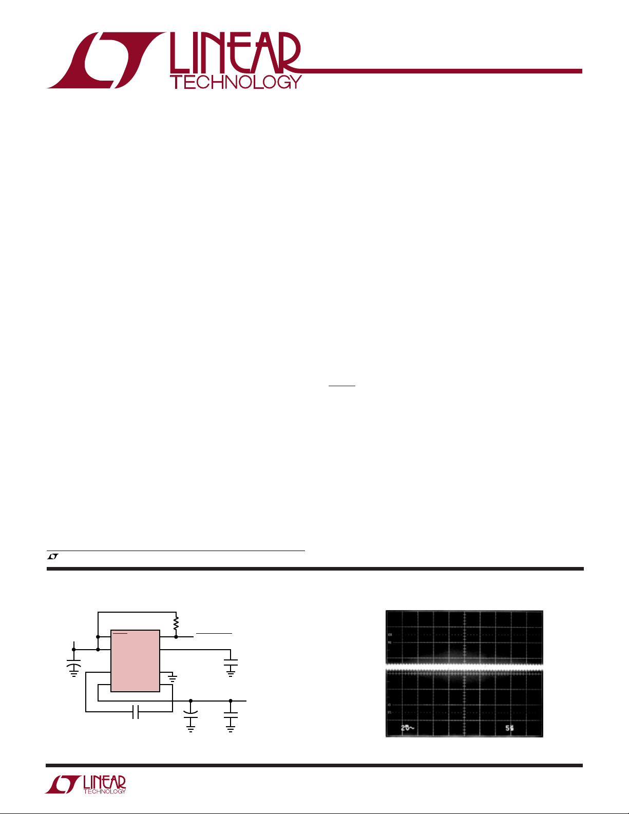
TYPICAL APPLICATIO
R1
10k
8
7
6
5
–
POWER VALID
C
OUT
+
10µF
P-P
2.2µF
C
IN
1
2
3
4
SHDN
V
CC
LTC1550L-2
+
C1
V
OUT
C1
0.1µF
REG
CP
OUT
GND
C1
3.6V
+
Figure 1. –2V Generator with 1mV
C
CP
0.1µF
V
OUT
I
LOAD
C
L
0.1µF
Noise
= –2V
= 5mA
1550L/51L TA01
Both fixed voltage and adjustable LTC1550L/LTC1551L
are available in 8-lead MSOP and SO plastic packages: the
adjustable LTC1550L is also available in a 16-pin SSOP
with the REG pin.
V
Output Noise and Ripple
OUT
V
OUT
AC COUPLED
2mV/DIV
5µs/DIV 1550L/51L TA01a
1
Page 2
LTC1550L/LTC1551L
WW
W
ABSOLUTE MAXIMUM RATINGS
U
(Note 1)
Supply Voltage ...................................................... 5.5V
Output Voltage............................. 0.3V to (VCC – 10.5V)
Total Voltage, VCC to CP
..........................................
OUT
10.8V
Input Voltage (SHDN Pin) ........... –0.3V to (VCC + 0.3V)
Input Voltage (REG Pin) ............................. –0.3V to 6V
Output Short-Circuit Duration.............................. 30 sec
U
W
U
PACKAGE/ORDER INFORMATION
TOP VIEW
1
SHDN*
2
V
CC
+
3
C1
4
V
OUT
MS8 PACKAGE
8-LEAD PLASTIC MSOP
*SHDN FOR LTC1550L, SHDN FOR LTC1551L
*FOR ADJUSTABLE VERSION
T
= 150°C, θJA = 200°C/W
JMAX
ORDER PART NUMBER
LTC1550LCMS8
LTC1550LCMS8-2
LTC1550LCMS8-2.5
LTC1550LCMS8-4.1
MS8 PART MARKING
LTEG
LTGR
LTFV
LTEH
8
REG (ADJ*)
7
CP
OUT
6
GND
–
5
C1
LTC1551LCMS8
LTC1551LCMS8-4.1
LTFQ
LTFT
SHDN*
V
CC
C1
V
OUT
*SHDN FOR LTC1550L, SHDN FOR LTC1551L
ORDER PART NUMBER
Commercial Temperature Range ................. 0°C to 70°C
Extended Commercial Operating
Temperature Range (Note 3) .............. –40°C to 85°C
Industrial Temperature Range ................ – 40°C to 85°C
Storage Temperature Range ................ –65°C to 150°C
Lead Temperature (Soldering, 10 sec)................. 300°C
TOP VIEW
1
2
+
3
4
S8 PACKAGE
8-LEAD PLASTIC SO
*FOR ADJUSTABLE VERSION
T
= 150°C, θJA = 135°C/W
JMAX
LTC1550LCS8
8
REG (ADJ*)
7
CP
6
GND
C1
5
OUT
–
NC
C1
NC
V
OUT
C1
PGND
AGND
NC
T
ORDER PART NUMBER
TOP VIEW
1
+
2
3
4
–
5
6
7
8
GN PACKAGE
16-LEAD PLASTIC SSOP
= 150°C, θJA = 150°C/W
JMAX
LTC1550LCS8-2
LTC1550LCS8-2.5
LTC1550LCS8-4.1
LTC1550LCGN
LTC1550LIGN
LTC1551LCS8
LTC1551LCS8-4.1
GN PART MARKING
1550L
1550LI
16
V
CC
15
SHDN
14
REG
13
NC
12
ADJ
11
CP
OUT
10
NC
9
NC
Consult factory for Military grade parts and additional voltage options.
ELECTRICAL CHARACTERISTICS
The ● denotes the specifications which apply over the full operating temperature range, otherwise specifications are at TA = 25°C.
VCC = 2.7V to 5.25V, C1 = C
SYMBOL PARAMETER CONDITIONS MIN TYP MAX UNITS
V
CC
V
REF
∆V
∆(VCC – V
I
S
Supply Voltage
(Adjustable, Fixed –2V)
(Fixed –2.5V)
(Fixed –4.1V) ● 4.5 5.25 V
Reference Voltage VCC = 5V, ADJ = GND, V
Reference Voltage I
REF
Line Regulation
OUT)
Supply Current VCC = 5V, V
= 0.1µF, C
CP
= 10µF, TA = 25°C unless otherwise specified. (Note 3)
OUT
= –V
REF
OUT
= 0mA, 2.7V ≤ VCC ≤ 5.25V 2.5 mV/V
OUT
= VCC (LTC1550L) or GND (LTC1551L) ● 3.65 7 mA
VCC = 5V, V
SHDN
= GND (LTC1550L) or VCC (LTC1551L) ● 0.2 10 µA
SHDN
● 2.7 5.25 V
● 3.05 5.25 V
1.225 V
2
Page 3
LTC1550L/LTC1551L
ELECTRICAL CHARACTERISTICS
The ● denotes the specifications which apply over the full operating temperature range, otherwise specifications are at TA = 25°C.
VCC = 2.7V to 5.25V, C1 = C
SYMBOL PARAMETER CONDITIONS MIN TYP MAX UNITS
f
OSC
V
OL
I
REG
V
IH
V
IL
I
IN
t
ON
V
OUT
V
OUT
V
OUT
V
OUT
V
OUT
V
OUT
V
OUT
I
SC
V
RIPPLE
Note 1: Absolute Maximum Ratings are those values beyond which the life
of a device may be impaired.
Note 2: All currents into device pins are positive; all currents out of device
pins are negative. All voltages are referenced to ground unless otherwise
specified. All typicals are given at T
Internal Oscillator Frequency 900 kHz
REG Output Low Voltage I
REG Sink Current V
SHDN Input High Voltage VCC = 5V ● 2V
SHDN Input Low Voltage VCC = 5V ● 0.8 V
SHDN Input Current V
Turn-On Time VCC = 5V, I
Output Regulation 2.7V ≤ VCC ≤ 5.25V, 0 ≤ I
(LTC1550L/LTC1551L) 2.8V ≤ V
Output Regulation 2.7V ≤ VCC ≤ 5.25V, 0 ≤ I
(LTC1550L/LTC1550L-2/ 3.1V ≤ V
LTC1551L) 3.75V ≤ VCC ≤ 5.25V, 0 ≤ I
Output Regulation 3.05V ≤ VCC ≤ 5.25V, 0 ≤ I
(LTC1550L/LTC1550L-2.5/ 3.45V ≤ V
LTC1551L) 4.1V ≤ VCC ≤ 5.25V, 0 ≤ I
Output Regulation 3.45V ≤ VCC ≤ 5.25V, 0 ≤ I
(LTC1550L/LTC1551L) 3.85V ≤ V
Output Regulation 3.9V ≤ VCC ≤ 5.25V, 0 ≤ I
(LTC1550L/LTC1551L) 4.2V ≤ V
Output Regulation 4.5V ≤ VCC ≤ 5.25V, 0 ≤ I
(LTC1550L/LTC1550L-4.1) 4.75V ≤ V
(LTC1551L/LTC1551L-4.1)
Output Regulation 4.8V ≤ VCC ≤ 5.25V, 0 ≤ I
(LTC1550L/LTC1551L)) 5.1V ≤ VCC ≤ 5.25V, 0 ≤ I
Output Short-Circuit Current V
Output Ripple Voltage 1mV
= 0.1µF, C
CP
= 25°C.
A
= 10µF, TA = 25°C unless otherwise specified. (Note 3)
OUT
= 1mA, VCC = 5V ● 0.1 0.8 V
REG
= 0.8V, VCC = 5V ● 410 mA
REG
= VCC (All LTC1550L Versions) ● 0.1 1 µA
SHDN
V
= VCC (All LTC1551L Versions) ● 520 µA
SHDN
= 10mA, –1.5V ≤ V
OUT
≤ 4.1V ● 15ms
OUT
(LTC1550L/LTC1551L)
V
= 5V, I
CC
= 5mA, V
OUT
= –4.5V ● 15ms
OUT
(LTC1550L/LTC1551L)
V
= 5V, I
CC
= 10mA, V
OUT
= –2V ● 15ms
OUT
(LTC1550L-2)
V
= 5V, I
CC
= 10mA, V
OUT
= –2.5V ● 15ms
OUT
(LTC1550L-2.5)
V
= 5V, I
CC
= 10mA, V
OUT
= –4.1V ● 15ms
OUT
(LTC1550L-4.1/LTC1551L-4.1)
≤ 5mA ● –1.537 –1.5 –1.463 V
≤ 5.25V, 0 ≤ I
CC
3.5V ≤ VCC ≤ 5.25V, 0 ≤ I
≤ 5.25V, 0 ≤ I
CC
≤ 5.25V, 0 ≤ I
CC
≤ 5.25V, 0 ≤ I
CC
4.5V ≤ VCC ≤ 5.25V, 0 ≤ I
≤ 5.25V, 0 ≤ I
CC
4.85V ≤ VCC ≤ 5.25V, 0 ≤ I
≤ 5.25V, 0 ≤ I
CC
= 0V, VCC = 5.25V ● 80 200 mA
OUT
OUT
≤ 10mA ● –1.537 –1.5 –1.463 V
OUT
≤ 20mA ● –1.537 –1.5 –1.463 V
OUT
≤ 5mA ● –2.05 – 2.0 –1.95 V
OUT
≤ 10mA ● –2.05 – 2.0 –1.95 V
OUT
≤ 20mA ● –2.05 – 2.0 –1.95 V
OUT
≤ 5mA ● –2.562 –2.5 –2.438 V
OUT
≤ 10mA ● –2.562 –2.5 –2.438 V
OUT
≤ 20mA ● –2.562 –2.5 –2.438 V
OUT
≤ 5mA ● –3.075 –3.0 –2.925 V
OUT
≤ 10mA ● –3.075 –3.0 –2.925 V
OUT
≤ 20mA ● –3.075 –3.0 –2.925 V
OUT
≤ 5mA ● –3.587 –3.5 –3.413 V
OUT
≤ 10mA ● –3.587 –3.5 –3.413 V
OUT
≤ 20mA ● –3.587 –3.5 –3.413 V
OUT
≤ 5mA ● –4.203 –4.1 –3.998 V
OUT
≤ 10mA ● –4.203 –4.1 –3.998 V
OUT
≤ 5mA ● –4.613 –4.5 –4.388 V
OUT
≤ 10mA ● –4.613 –4.5 –4.388 V
OUT
Note 3: The LTC1550LC/LTC1551LC are guaranteed to meet specified
performance from 0°C to 70°C and are designed, characterized and
expected to meet these extended temperature limits, but are not tested at
–40°C and 85°C. The LTC1550LI is guaranteed to meet the extended
temperature limits.
3
Page 4
LTC1550L/LTC1551L
1.24
1.238
1.236
1.234
1.232
1.230
1.228
1.226
1.224
1.222
1.220
1.218
V
CC
+ |V
OUT
| (V)
456789104.5 5.5 6.5 7.5 8.5 9.5
REFERENCE VOLTAGE (V)
1550L/51L G06
TA = 25°C
W
U
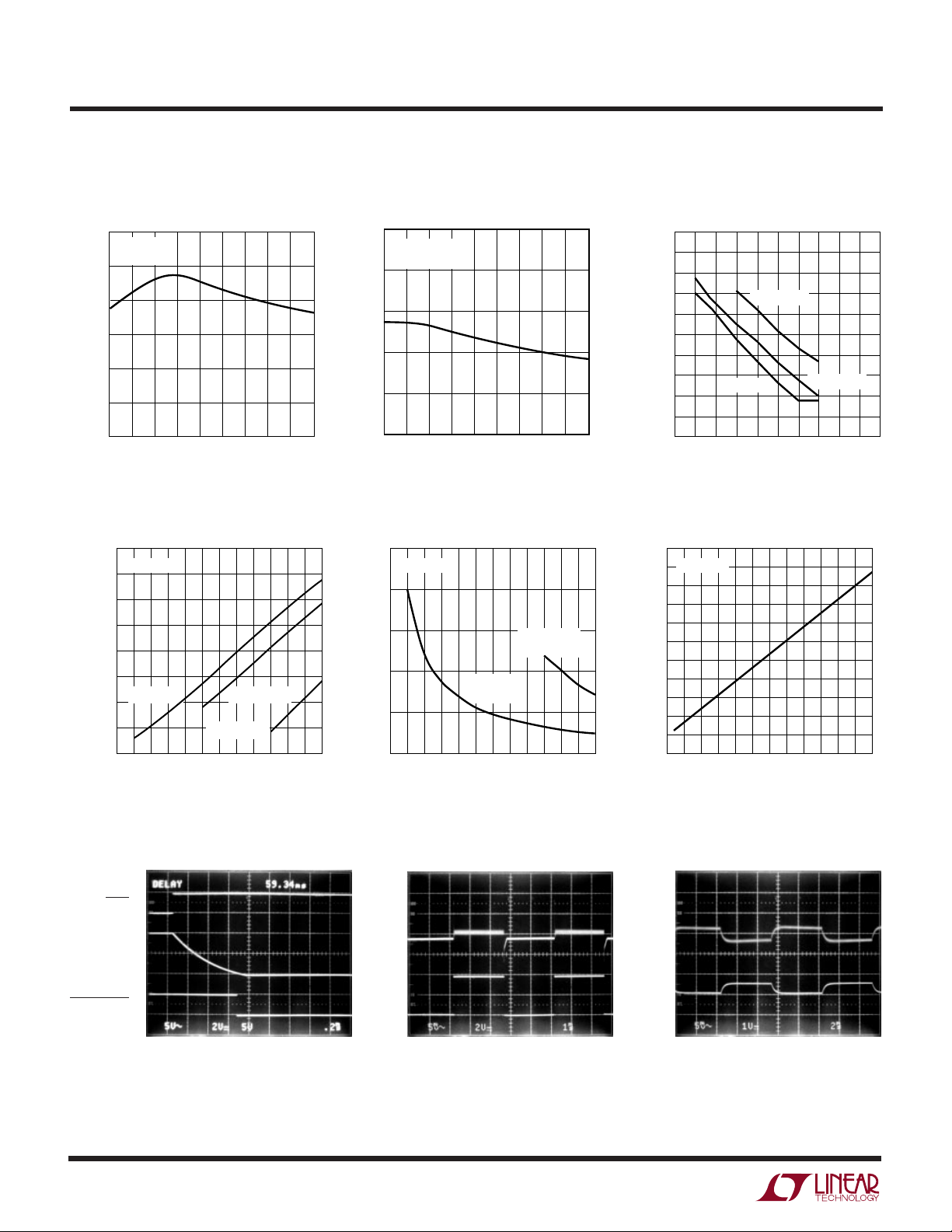
TYPICAL PERFORMANCE CHARACTERISTICS
Oscillator Frequency vs
Temperature
975
VCC = 5V
= –4.1V
V
OUT
925
875
825
775
OSCILLATOR FREQUENCY (kHz)
725
675
–55 –35 –15 5 25 45 65 85 105 125
TEMPERATURE (˚C)
Maximum Output Current
vs Supply Voltage
80
TA = 25°C
70
60
50
40
30
V
= –2V V
OUT
20
MAXIMUM OUTPUT CURRENT (mA)
10
0
2.25 2.75 3.25 3.75 4.25 4.75 5.25
SUPPLY VOLTAGE (V)
V
OUT
= –2.5V
OUT
= –4.1V
1550L/51L G01
1550L/51L G04
Supply Current vs Temperature
5.0
VCC = 5V
= –4.1V
V
OUT
4.5
4.0
3.5
SUPPLY CURRENT (mA)
3.0
2.5
–55 –35 –15 5 25 45 65 85 105 125
2.5
2.0
1.5
1.0
START-UP TIME (ms)
0.5
0
2.25 2.75 3.25 3.75 4.25 4.75 5.25
TEMPERATURE (°C)
TA = 25°C
V
OUT
R
L
V
= –2V
OUT
= 390Ω
R
L
SUPPLY VOLTAGE (V)
= 820Ω
1550L/51L G02
= –4.1V
1550L/51L G05
Minimum Required V
vs V
6.0
5.6
5.2
4.8
4.4
4.0
3.6
3.2
2.8
POSITIVE SUPPLY VOLTAGE (V)
2.4
2.0
–5
and I
OUT
OUT
I
I
= 5mA
OUT
–4
–3
OUTPUT VOLTAGE (V)
OUT
= 20mA
–2
Reference Voltage vs VCC + |V
CC
I
OUT
= 10mA
–1
1550L/51L G03
OUT
0
|Start-Up Time vs Supply Voltage
Startup Time (LTC1550L Shown)
5V
SHDN
0V
0V
V
OUT
POWER VALID
4
–4.1V
5V
0V
0.2ms/DIV 1550/51 G07
Load Transient Response
(See Figure 3, VCC = 5V)
V
OUT
5mV/DIV
AC
COUPLED
10mA
I
OUT
0mA
1ms/DIV
1550/51 G08
V
5mV/DIV
COUPLED
5.25V
V
CC
4.75V
Line Transient Response
(See Figure 3, IL = 10mA)
OUT
AC
2ms/DIV
1550/51 G09
Page 5

W
FREQUENCY (kHz)
1
0.01
NOISE (µV/√Hz)
1
0.1
10
10 100
1550L/51L G15
VCC = 5V
I
L
= 5mA
C
IN
= 2.2µF
C
OUT
= 10µF
C
L
= 0.1µF
U
TYPICAL PERFORMANCE CHARACTERISTICS
LTC1550L/LTC1551L
Output Spectrum (*See Figure 1)
90
80
70
60
50
40
30
NOISE (dBµV)
20
10
0
–10
100k
1M 10M
FREQUENCY (Hz)
Spot Noise (See Figure 3)
10
1
NOISE (µV/√Hz)
VCC = 5V
0.1
= 5mA
I
L
= 2.2µF
C
IN
= 4.7µF
C
OUT
= 0.1µF
C
L
0.01
1
10 100
FREQUENCY (kHz)
1550L/51L G10
1550L/51L G13
Spot Noise (*See Figure 1) Output Spectrum (See Figure 3)
10
1
NOISE (µV/√Hz)
0.1
0.01
1
10 100
FREQUENCY (kHz)
Output Spectrum (See Figure 3)
90
VCC = 5V
80
= 5mA
I
L
2.2µF
C
70
IN
C
= 10µF
OUT
60
= 0.1µF
C
L
50
40
30
NOISE (dBµV)
20
10
0
–10
100k
1M 10M
FREQUENCY (Hz)
1550 /51L G11
1550L/51L G14
90
VCC = 5V
80
= 5mA
I
L
C
= 2.2µF
70
IN
= 4.7µF
C
OUT
60
= 0.1µF
C
L
50
40
30
NOISE (dBµV)
20
10
0
–10
100k
FREQUENCY (Hz)
Spot Noise (See Figure 3)
1M 10M
1550L/51L G12
* On first page of data sheet.
5
Page 6

LTC1550L/LTC1551L
UUU
PIN FUNCTIONS
SHDN: Shutdown (TTL Compatible). This pin is active low
(SHDN) for the LTC1550L and active high (SHDN) for the
LTC1551L. When this pin is at VCC (GND for LTC1551L),
the LTC1550L operates normally. When SHDN is pulled
low (SHDN pulled high for LTC1551L), the LTC1550L
enters shutdown mode. In shutdown, the charge pump
stops, the output collapses to 0V, and the quiescent
current drops typically to 0.2µA. The SHDN pin for the
LTC1550L is a high impedance input and has no internal
pull-up. The user must supply a resistor or current source
pull-up to default the LTC1550L into normal operation.
The SHDN pin for the LTC1551L has an internal 5µA
typical pull-down that defaults the LTC1551L into normal
operation.
VCC: Power Supply. VCC requires an input voltage between
2.7V and 5.25V. Certain combinations of output voltage
and output load current may place additional restrictions
on the required input voltage. Consult the Electrical Characteristics table and Typical Performance Characteristics
for guaranteed test points. The difference between the
input voltage and output should not exceed 10.5V or
damage to the chip may occur. VCC must be bypassed
directly to PGND (GND for 8-pin packages) with at least a
0.1µF capacitor placed in close proximity to the chip. A 1µF
or larger low ESR bypass capacitor is recommended to
minimize noise and ripple at the output. A surface mount
ceramic capacitor is recommended.
+
C1
: C1 Positive Input. Connect a 0.1µF capacitor between
C1+ and C1–.
V
: Negative Voltage Output. This pin must be bypassed
OUT
with a 4.7µF or larger capacitor to ensure regulator loop
stability. LTC recommends at least 10µF to achieve the
specified output ripple. The output capacitor should be a
moderate ESR capacitor, and not a very low ESR capacitor, as the zero in the feedback loop (formed by the ESR
and the output capacitor) provides phase lead to the linear
regulator feedback loop. Using very low ESR output capacitors will result in the output oscillating. A low ESR
0.1µF capacitor is recommended in parallel with the main
output capacitor to minimize high frequency spikes at the
output. The ground connection for the output capacitor
should connect directly to the VCC and CP
capacitors, as well as to the GND of the LTC1550L/
LTC1551L. LTC recommends a separate trace for the V
capacitor ground connection to minimize noise.
–
C1
: C1 Negative Input. Connect a 0.1µF capacitor from
C1+ to C1–.
GND: Ground. Connect to a low impedance ground. A
ground plane will help minimize regulation errors.
CP
: Negative Charge Pump Output. This pin requires a
OUT
0.1µF storage capacitor to ground. In order to achieve
ripple on the output voltage of less than 1mV, the ground
connection for the CP
bottom of the VCC bypass capacitor and at the GND pin of
the LTC1550L/LTC1551L. This minimizes the AC current
path for the charge pump.
REG: This is an open-drain output that pulls low when the
output voltage is within 5% of the set value. It will sink 4mA
to ground with a 5V supply. The external circuitry must
provide a pull-up or REG will not swing high. The voltage
at REG may exceed VCC and can be pulled up to 6V above
ground without damage. For the LTC1550L adjustable
voltage version, the REG pin is only available in the 16-lead
GN package.
ADJ (for adjustable versions): This is the feedback point
for the external resistor divider string. Connect a divider
string from GND to V
ADJ. Note that the resistor string needs to be connected
“upside-down” from a negative regulator. See the Applications Information section for hook-up details.
GN PACKAGE ONLY
PGND: Power Ground. Connect to a low impedance ground.
PGND should be connected to the same potential as
AGND.
AGND: Analog Ground. Connect to a low impedance
ground. AGND should be connected to a ground plane to
minimize regulation errors.
NC: No Internal Connection.
capacitor must tie directly to the
OUT
with the divided tap connected to
OUT
OUT
bypass
OUT
6
Page 7

BLOCK DIAGRAM
LTC1550L/LTC1551L
W
*SHDN
V
CC
S1
CLK
900kHz
S2
S3
*SHDN FOR LTC1550L, SHDN FOR LTC1551L
** FIXED OUTPUT VERSIONS ONLY
C1
C1
C1
S4
+
–
CHARGE
PUMP
C
CP
CP
1.225V
OUT
LINEAR
REGULATOR
58mV
1.167V
+
C
OUT
V
OUT
+
–
**
**
+
COMP2
ADJ
REG
–
1550L/51L BD
U
WUU
APPLICATIONS INFORMATION
OVERVIEW
The LTC1550L/LTC1551L are switched capacitor, inverting
charge pumps with internal linear post-regulators. The
LTC1550L/LTC1551L provide a regulated, low ripple output
at up to 20mA load current with the appropriate input
voltage as output load current depends on the input/
output voltage combination. Consult the graph provided in
the Typical Performance Characteristics section and the
Electrical Characteristics table for guaranteed test points.
The LTC1550L/LTC1551L are ideal for use as bias voltage
generators for GaAs transmitter FETs in portable RF and
cellular telephone applications. The LTC1550L features an
active-low Shutdown pin (SHDN) that drops quiescent
current to below 1µA. The LTC1551L is identical to the
LTC1550L, except that the Shutdown pin is active-high
(SHDN). All members of the LTC1550L/LTC1551L family
feature a 900kHz charge pump frequency. The LTC1550L/
LTC1551L come standard with fixed –4.1V, –2.5V, –2V
and adjustable output voltages. The LTC1550L/LTC1551L
can be configured for other fixed output voltages; contact
Linear Technology for more information.
7
Page 8

LTC1550L/LTC1551L
U
WUU
APPLICATIONS INFORMATION
The LTC1550L/LTC1551L consist of two major blocks
(see Block Diagram): an inverting charge pump and a
negative linear regulator. The charge pump uses two
external capacitors, C1 and CCP to generate a negative
voltage at CP
C1 on alternate phases of the internal 900kHz clock. C1 is
initially charged to VCC through switches S1 and S3. When
the internal clock changes phase, S1 and S3 open and S2
and S4 close, shorting the positive side of C1 to ground.
This forces the negative side of C1 below ground, and
charge is transferred to CCP through S4. As this cycle
repeats, the magnitude of the negative voltage approaches
VCC. The 900kHz internal clock frequency helps keep noise
out of the 400kHz to 600kHz IF bands commonly used by
portable radio frequency systems and reduces the size of
the external capacitors required. Most applications can
use standard 0.1µF ceramic capacitors for C1 and CCP.
Increasing C1 and CCP beyond 0.1µF has little effect on the
output ripple or the output current capacity of the
LTC1550L/LTC1551L.
The negative voltage at CP
negative regulator block. This block consists of an
N-channel MOSFET pass device and a feedback amplifier
that monitors the output voltage and compares it to the
internal reference. The regulated output appears at the
V
pin. The regulation loop is optimized for fast tran-
OUT
sient response, enabling it to remove most of the switching artifacts present at the CP
typically below 1mV
and 10mA. The output voltage is set by a pair of internal
divider resistors for the fixed voltage versions. The Nchannel pass device minimizes dropout, allowing the
output to remain in regulation with supply voltages as low
as 2.7V for an output voltage of –2V. An output capacitor
of at least 4.7µF from V
the regulator loop stable; for optimum stability and minimum output ripple, at least 10µF is recommended.
Adjustable Hook-Up
For the adjustable LTC1550L/LTC1551L, the output voltage is set with a resistor divider from GND to V
(Figure␣ 2). Note that the internal reference and the internal
feedback amplifier are set up as a positive-output regulator referenced to the V
. It operates by charging and discharging
OUT
supplies the input to the
OUT
pin. Output ripple is
OUT
with output loads between 0mA
P-P
to ground is required to keep
OUT
pin, not as a negative regulator
OUT
OUT
PGND, AGND
R1
V
ADJ
OUT
R2
V
OUT
= –1.225V
R1 + R2
()
R2
1550L/51L • F02
LTC1550L
Figure 2. External Resistor Connections
referenced to ground. The output resistor divider must be
set to provide 1.225V at the ADJ pin with respect to V
OUT
.
For example, a –3V output would require a 17.4k resistor
from GND to ADJ, and a 12.1k resistor to V
OUT
.
CAPACITOR SELECTION
The LTC1550L/LTC1551L requires four external capacitors: an input bypass capacitor, two 0.1µF charge pump
capacitors and an output filter capacitor. The overall
behavior of the LTC1550L/LTC1551L is strongly affected
by how the capacitors are used, and by how the capacitors
are laid out on the printed circuit board (PCB). In particular, the output capacitor’s value and ESR have a significant
effect on the output ripple and noise performance. In
addition, the ground connections for the VCC bypass
capacitor, the CP
capacitor and the V
OUT
bypass ca-
OUT
pacitor must employ star-ground techniques at the GND
pin of the LTC1550L/LTC1551L. Proper capacitor selection is critical for optimum performance of the LTC1550L/
LTC1551L.
Output Ripple vs Output Capacitor
Figure 4 shows the effect of using different output capacitor values on the LTC1550L/LTC1551L output ripple.
These curves are taken using the LTC1551L circuit in
Figure 3, with CIN = 2.2µF and I
= 5mA. The upper
LOAD
curve shows the performance with a standard tantalum
capacitor alone and the lower curve shows that of the
tantalum capacitor in parallel with a 0.1µF ceramic capaci-
tor. As a general rule, larger output capacitors provide
lower output ripple. To keep output voltage ripple below
1mV
, 10µF, or greater, in parallel with a 0.1µF ceramic
P–P
capacitor is required. To guarantee loop stability under all
conditions, a minimum of 4.7µF is required at the output.
8
Page 9

LTC1550L/LTC1551L
OUTPUT CAPACITANCE (µF)
8
7
6
5
4
3
2
1
0
10
1550L/51L F04
OUTPUT RIPPLE (mV
P-P
)
1
100
VCC = 5V
T
A
= 25°C
C
IN
= 2.2µF
WITHOUT 0.1µF
WITH 0.1µF
U
WUU
APPLICATIONS INFORMATION
Figure 4 shows a marked decrease in peak-to-peak output
ripple when a 0.1µF ceramic capacitor is added in parallel
with the tantalum output capacitor. The additional ripple
with the tantalum output capacitor alone is mostly very
high order harmonics of the 900kHz clock, which appear
as sharp "spikes" at the output. The energy in these spikes
is very small and they do not contribute to the RMS output
voltage, but their peak-to-peak amplitude can be several
millivolts under some conditions. A 0.1µF ceramic capaci-
tor has significantly lower impedance at the spike frequency than a large tantalum capacitor, and eliminates
most of these left-over switching spikes that the tantalum
capacitor leaves behind. Figure 5 and 6 show scope photos
of the output of Figure 4 with and without the additional
ceramic capacitor at the output.
R1
10k
8
7
C
CP
6
5
–
C
OUT
+
10µF
0.1µF
C
L
0.1µF
V
OUT
–4.1V
1550L/51L F03
C
IN
2.2µF
1
2
3
4
SHDN
V
CC
+
C1
V
OUT
LTC1551L
C1
0.1µF
REG
CP
OUT
GND
C1
V
CC
+
A series RC or LC filter can reduce high frequency output
noise even further. Due to the high 900kHz switching
frequency, not much R or L is required; a ferrite bead or a
relatively long PC board trace in series with 0.1µF ceramic
capacitor will usually keep the output ripple well below
1mV
. Figure 1 shows an example of an ultralow noise
P-P
–2V generator. The corresponding spectrum and spot
noise plots for this circuit are shown in the Typical Performance Characteristics section.
AC COUPLE
5mV/DIV
Figure 3. Output Ripple Test Circuit
V
OUT
5µs/DIV 1550L/51L F05
Figure 5. Output Ripple with 10µF Tantalum Capacitor
Figure 4. Output Ripple vs Output Capacitance
V
OUT
AC COUPLE
2mV/DIV
10µs/DIV 1550L/51L F06
Figure 6. Output Ripple with 10µF Tantalum
Capacitor Paralleled with 0.1µF Ceramic Capacitor
9
Page 10

LTC1550L/LTC1551L
U
WUU
APPLICATIONS INFORMATION
Output Ripple vs Input Bypass Capacitor
The input bypass capacitor (CIN) can also have a fairly
significant impact on the output ripple. CIN provides most
of the LTC1550L/LTC1551L’s supply current while it is
charging the flying capacitor (C1). Inadequate input
bypassing can cause the VCC supply to dip when the
charge pump switches, causing the output linear regulator
to momentarily stop regulating. CIN should be mounted as
close to the LTC1550L/LTC1551L VCC and GND pins as
possible and its value should be significantly larger than
8
VCC = 5V
7
T
= 25°C
A
= 10µF
C
OUT
)
6
P-P
5
4
3
OUTPUT RIPPLE (mV
2
1
0
0.1
Figure 7. Output Ripple vs Input Bypass Capacitance
1 10 100
INPUT CAPACITANCE (µF)
C1. Surface mount tantalum or ceramic capacitors with
low ESR generally provide adequate performance. Figure␣ 7
shows the LTC1550L/LTC1551L peak-to-peak output ripple
vs CIN, taken using the test circuit in Figure 3 with I
at 5mA. C
is a 10µF in parallel with a 0.1µF ceramic
OUT
LOAD
set
capacitor.
A 2.2µF surface mount ceramic capacitor at VCC generally
provides adequate output ripple performance for most
applications.
1550L/51L F08
TYPICAL APPLICATION
CC
+
≤ 5.25V
C
2.2µF
4.5V ≤ V
10
U
–4.1V Output GaAs FET Bias Generator
1
SHDN
2
V
CC
IN
LTC1550L-4.1
3
+
C1
4
V
OUT
C1
0.1µF
8
REG
7
CP
OUT
GND
C1
6
5
–
C
0.1µF
CP
C
+
10µF
OUT
–4.1V BIAS
C
L
0.1µF
GaAs
TRANSMITTER
1550L/51L TA02
Page 11

PACKAGE DESCRIPTION
(
LTC1550L/LTC1551L
U
Dimensions in inches (millimeters) unless otherwise noted.
GN Package
16-Lead Plastic SSOP (Narrow 0.150)
(LTC DWG # 05-08-1641)
0.189 – 0.196*
(4.801 – 4.978)
16
15
14
12 11 10
13
0.009
(0.229)
9
REF
0.229 – 0.244
(5.817 – 6.198)
0.015
± 0.004
(0.38 ± 0.10)
0.007 – 0.0098
(0.178 – 0.249)
0.016 – 0.050
(0.406 – 1.270)
* DIMENSION DOES NOT INCLUDE MOLD FLASH. MOLD FLASH
SHALL NOT EXCEED 0.006" (0.152mm) PER SIDE
** DIMENSION DOES NOT INCLUDE INTERLEAD FLASH. INTERLEAD
FLASH SHALL NOT EXCEED 0.010" (0.254mm) PER SIDE
0° – 8° TYP
× 45°
0.053 – 0.068
(1.351 – 1.727)
0.008 – 0.012
(0.203 – 0.305)
MS8 Package
8-Lead Plastic MSOP
(LTC DWG # 05-08-1660)
0.040
± 0.006
SEATING
PLANE
(1.02 ± 0.15)
0.012
(0.30)
0.0256
REF
(0.65)
BSC
0.152mm) PER SIDE
0.007
(0.18)
0.021
± 0.006
(0.53 ± 0.015)
* DIMENSION DOES NOT INCLUDE MOLD FLASH, PROTRUSIONS OR GATE BURRS. MOLD FLASH,
PROTRUSIONS OR GATE BURRS SHALL NOT EXCEED 0.006" (0.152mm) PER SIDE
** DIMENSION DOES NOT INCLUDE INTERLEAD FLASH OR PROTRUSIONS.
INTERLEAD FLASH OR PROTRUSIONS SHALL NOT EXCEED 0.006"
° – 6° TYP
0
0.034 ± 0.004
(0.86 ± 0.102)
0.006 ± 0.004
(0.15 ± 0.102)
12
3
0.118 ± 0.004*
(3.00 ± 0.102)
0.193 ± 0.006
(4.90 ± 0.15)
0.150 – 0.157**
(3.810 – 3.988)
5
4
678
0.004 – 0.0098
(0.102 – 0.249)
0.0250
(0.635)
BSC
GN16 (SSOP) 1098
8
7
6
5
0.118 ± 0.004**
(3.00 ± 0.102)
MSOP (MS8) 1098
12
4
3
Information furnished by Linear Technology Corporation is believed to be accurate and reliable.
However, no responsibility is assumed for its use. Linear Technology Corporation makes no representation that the interconnection of its circuits as described herein will not infringe on existing patent rights.
11
Page 12

LTC1550L/LTC1551L
TYPICAL APPLICATION
U
1mV
Ripple, –2V Output GaAs FET Bias Generator
P-P
2.7V ≤ V
≤ 5.25V
CC
+
C
2.2µF
PACKAGE DESCRIPTION
0.010 – 0.020
(0.254 – 0.508)
0.008 – 0.010
(0.203 – 0.254)
*
DIMENSION DOES NOT INCLUDE MOLD FLASH. MOLD FLASH
SHALL NOT EXCEED 0.006" (0.152mm) PER SIDE
**
DIMENSION DOES NOT INCLUDE INTERLEAD FLASH. INTERLEAD
FLASH SHALL NOT EXCEED 0.010" (0.254mm) PER SIDE
× 45°
0.016 – 0.050
(0.406 – 1.270)
0.053 – 0.069
(1.346 – 1.752)
0°– 8° TYP
0.014 – 0.019
(0.355 – 0.483)
1
SHDN
2
V
IN
3
C1
4
V
CC
LTC1550L-2
+
OUT
C1
0.1µF
REG
CP
OUT
GND
C1
10k
8
REG
7
C
CP
6
5
–
0.1µF
C
+
10µF
OUT
–2V
C
L
0.1µF
GaAs
TRANSMITTER
1550L/51L TA03
U
Dimensions in inches (millimeters) unless otherwise noted.
S8 Package
8-Lead Plastic Small Outline (Narrow 0.150)
(LTC DWG # 05-08-1610)
8
0.004 – 0.010
(0.101 – 0.254)
0.228 – 0.244
(5.791 – 6.197)
1
TYP
0.050
(1.270)
BSC
0.189 – 0.197*
(4.801 – 5.004)
7
6
3
2
5
0.150 – 0.157**
(3.810 – 3.988)
4
SO8 1298
RELATED PARTS
PART NUMBER DESCRIPTION COMMENTS
LT®1054 Switched-Capacitor Voltage Converter with Regulator 100mA Switched-Capacitor Converter
LTC1261 Switched-Capacitor Regulated Voltage Inverter Selectable Fixed Output Voltages
LTC1261L Switched-Capacitor Regulated Voltage Inverter Adjustable and Fixed Output Voltages, Up to 20mA I
LTC1429 Clock-Synchronized Switched-Capacitor Voltage Inverter Synchronizable Up to 2MHz System Clock
LTC1514/LTC1515 Step-Up/Step-Down Switched-Capacitor DC/DC Converters VIN 2V to 10V, Adjustable or Fixed V
LTC1516 Micropower Regulated 5V Charge Pump DC/DC Converter I
LTC1522 Micropower Regulated 5V Charge Pump DC/DC Converter I
LTC1550/LTC1551 Low Noise, Switched-Capacitor Regulated Voltage Inverters 900kHz Charge Pump, 1mV
= 20mA (VIN ≥ 2V), I
OUT
= 10mA (VIN ≥ 2.7V), I
OUT
= 50mA (VIN ≥ 3V)
OUT
= 20mA (VIN ≥ 3V)
OUT
Ripple
P-P
OUT
, I
OUT
to 50mA
LTC1555/LTC1556 SIM Power Supply and Level Translator Step-Up/Step-Down SIM Power Supply and Level Translators
LT1611 1.4MHz Inverting Mode Switching Regulator –5V at 150mA from a 5V Input, 5-Lead SOT-23
LT1614 Inverting 600kHz Switching Regulator with Low-Battery Detector –5V at 200mA from a 5V Input, MSOP
LTC1754-5 Micropower, Regulated 5V Charge Pump with Shutdown in SOT-23 ICC = 13µA, I
= 50mA (VIN ≥ 3V), I
OUT
= 25mA (VIN ≥ 2.7V)
OUT
15501lf LT/TP 0300 4K • PRINTED IN USA
Linear Technology Corporation
12
1630 McCarthy Blvd., Milpitas, CA 95035-7417
(408) 432-1900 ● FAX: (408) 434-0507
●
www.linear-tech.com
LINEAR TECHNOLOGY CORPORATION 1996
OUT
, MSOP
 Loading...