

Page 1
Final Electrical Specifications
FEATURES
LTC1535
Isolated RS485 Transceiver
August 1999
U
DESCRIPTIO
■
UL Rated Isolated RS485: 2500V
■
Half- or Full-Duplex
■
Eliminates Ground Loops
■
350kBd Maximum Data Rate
■
Self-Powered with 400kHz Converter
■
Fail-Safe Output High for Open or
RMS
Shorted Receiver Inputs
■
Short-Circuit Current Limit
■
Slow Slew Rate Control
■
68kΩ Input Impedance Allows Up to 128 Nodes
■
Thermal Shutdown
■
8kV ESD Protection On Driver Outputs and Receiver
Inputs
U
APPLICATIO S
■
Isolated RS485 Receiver/Driver
■
RS485 with Large Common Mode Voltage
■
Breaking RS485 Ground Loops
■
Multiple Unterminated Line Taps
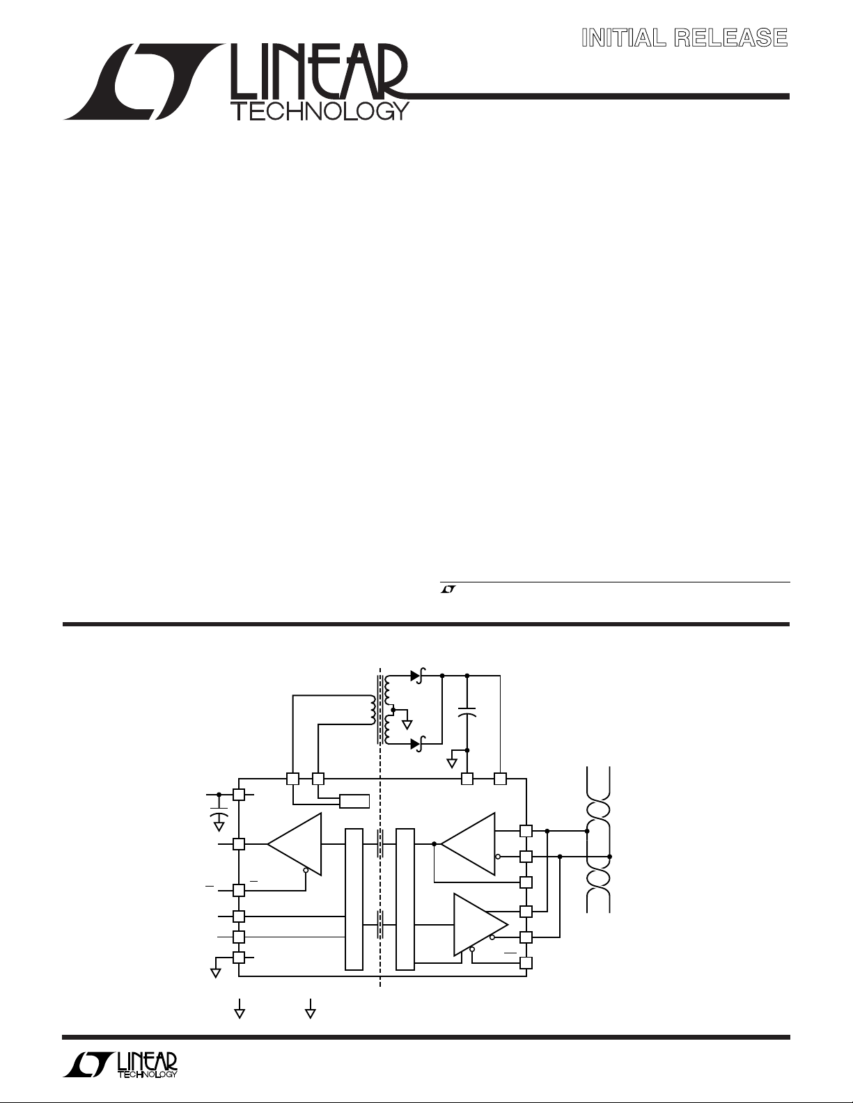
The LTC®1535 is an isolated RS485 full-duplex differential
line transceiver. Isolated RS485 is ideal for systems where
the ground loop is broken to allow for much larger common mode voltage ranges. An internal capacitive isolation
barrier provides 2500V
of isolation between the line
RMS
transceiver and the logic level interface. The powered side
contains a 400kHz push-pull converter to power the isolated RS485 transceiver. Internal full-duplex communication occurs through the capacitive isolation barrier. The
transceiver meets RS485 and RS422 requirements.
The driver and receiver feature three-state outputs, with
the driver maintaining high impedance over the entire
common mode range. The drivers have short-circuit current limits in both directions and a slow slew rate select to
minimize EMI or reflections. The 68kΩ receiver input
allows up to 128 node connections. A fail-safe feature
defaults to a high output state when the receiver inputs are
open or shorted.
, LTC and LT are registered trademarks of Linear Technology Corporation.
TYPICAL APPLICATIO
1
1
28
27
26
25
4
1
V
RO
RE
DE
DI
GND
LOGIC COMMON
1
V
CC
10µF
+
RO
RE
DE
DI
U
ST1 ST2
CC
**
CTX02-14659
32
400kHz
FLOATING RS485 COMMON ** TRANSFORMER
2
1/2 BAT54C
2
1/2 BAT54C
2
COILTRONICS (561) 241-7876
+
GND2
10µF
1411
V
CC2
A
R
D
B
RO2
Y
Z
SLO
1535 TA01
16
15
17
13
12
18
TWISTED-PAIR
CABLE
Information furnished by Linear Technology Corporation is believed to be accurate and reliable.
However, no responsibility is assumed for its use. Linear Technology Corporation makes no representation that the interconnection of its circuits as described herein will not infringe on existing patent rights.
1
Page 2
LTC1535
WW
W
U
ABSOLUTE AXI U RATI GS
(Note 1)
VCC to GND ................................................................ 6V
V
to GND2 ............................................................ 8V
CC2
Control Input Voltage to GND ...... –0.3V to (VCC + 0.3V)
Driver Input Voltage to GND ........ –0.3V to (VCC + 0.3V)
Driver Output Voltage
(Driver Disabled) to GND2 ..............(V
Driver Output Voltage
(Driver Enabled) to GND2 ............... (V
Receiver Input Voltage to GND2 ............................ ±14V
Receiver Output Voltage .............. –0.3V to (VCC + 0.3V)
Operating Temperature Range ..............0°C ≤ TA ≤ 70°C
Lead Temperature (Soldering, 10 sec)..................300°C
– 13V) to 13V
CC2
– 13V) to 10V
CC2
UUW
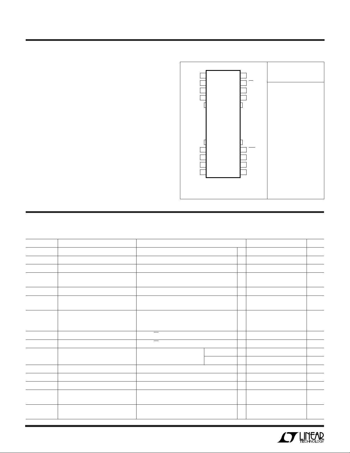
PACKAGE/ORDER I FOR ATIO
TOP VIEW
1
V
CC
2
ST1
3
ST2
4
GND
11
GND2
12
Z
13
Y
14
V
CC2
SW PACKAGE
28-LEAD PLASTIC SO WIDE
T
= 125°C, θJA = 125°C/W
JMAX
Consult factory for Industrial and Military grade parts.
28
RO
27
RE
26
DE
25
DI
18
SLO
17
RO2
16
A
15
B
ORDER PART
NUMBER
LTC1535CSW
ELECTRICAL CHARACTERISTICS
temperature range, otherwise specifications are at T
SYMBOL PARAMETER CONDITIONS MIN TYP MAX UNITS
V
CC
V
CC2
I
CC
I
CC2
V
OD1
V
OD2
I
OSD1
V
IH
V
IL
I
IN
V
TH
∆V
R
IN
V
OH
V
OL
TH
VCC Supply Range ● 4.5 5.5 V
V
Supply Range ● 4.5 7.5 V
CC2
VCC Supply Current No Load ● 13 18 mA
V
Supply Current R = 27Ω, Figure 1 ● 63 73 mA
CC2
Differential Driver Output No Load ● 5V
Differential Driver Output R = 50Ω (RS422) Note 2 ● 2V
Driver Short-Circuit Current
= HIGH –7V ≤ VCM ≤ 10V ● 75 100 135 mA
V
OUT
V
= LOW –7V ≤ VCM ≤ 10V ● 75 100 135 mA
OUT
Logic Input High Voltage DE, DI, RE VCC = 4.5V ● 2V
Logic Input Low Voltage DE, DI, RE VCC = 4.5V ● 0.8 V
Input Current (A, B) Note 3 VIN = 12V ● 0.25 mA
Receiver Input Threshold –7V ≤ VCM ≤ 12V, Note 4 ● –200 –90 –10 mV
Receiver Input Hysteresis –7V ≤ VCM ≤ 12V ● 10 30 70 mV
Receiver Input Impedance ● 50 68 85 kΩ
RO Output High Voltage IRO = –4mA, VCC = 4.5V ● 3.7 4.0 V
RO Output Low Voltage IRO = 4mA, VCC = 4.5V ● 0.4 0.8 V
No Load
R = 27Ω(RS485), Figure 1
I
I
The ● denotes the specifications which apply over the full operating
= 25°C. 0°C ≤ TA ≤ 70°C, V
A
= –10mA, VCC = 4.5V 3.4 V
RO
= 10mA, VCC = 4.5V 0.9 V
RO
= 5V, V
CC
VIN = –7V ● –0.20 mA
= 5V unless otherwise noted.
CC2
● 712 mA
● 1.5 2 V
2
Page 3
LTC1535
ELECTRICAL CHARACTERISTICS
temperature range, otherwise specifications are at T
The ● denotes the specifications which apply over the full operating
= 25°C. 0°C ≤ TA ≤ 70°C, V
A
= 5V, V
CC
= 5V unless otherwise noted.
CC2
SYMBOL PARAMETER CONDITIONS MIN TYP MAX UNITS
I
V
V
f
R
R
I
I
V
V
V
OZ
OH2
OL2
SW
SWH
SWL
REL
REH
UVL
UVH
ISO
Driver Output Leakage 1 µA
RO2 Output High Voltage I
RO2 Output Low Voltage I
= –4mA, VCC = 4.5V ● 3.7 3.9 V
RO2
I
= –10mA, VCC = 4.5V 3.4 V
RO2
= 4mA, VCC = 4.5V ● 0.4 0.8 V
RO2
I
= 10mA, VCC = 4.5V 0.9 V
RO2
DC Converter Frequency ● 290 420 520 kHz
DC Converter R High VCC = 4.5V ● 46 Ω
DC Converter R Low VCC = 4.5V ● 2.5 5 Ω
RE Output Low Current RE Sink Current, Fault = 0 ● –40 –50 –80 µA
RE Output High Current RE Source Current, Fault = 1 ● 80 100 130 µA
Undervoltage Low Threshold RE Fault = 1, Note 5 ● 3.90 4.00 4.25 V
Undervoltage High Threshold RE Fault = 0, Note 5 ● 4.05 4.20 4.40 V
Isolation Voltage 1 Minute, Note 6 2500 V
1 Second 3000 V
RMS
RMS
U
SWITCHI G CHARACTERISTICS
temperature range, otherwise specifications are at T
otherwise noted.
The ● denotes the specifications which apply over the full operating
= 25°C. 0°C ≤ TA ≤ 70°C, V
A
= 5V, V
CC
= 5V, R = 27Ω (RS485) unless
CC2
SYMBOL PARAMETER CONDITIONS MIN TYP MAX UNITS
t
SJ
f
MAX
t
PLH
t
PHL
tr, t
t
ZH
t
ZL
t
LZ
t
HZ
t
PLH
t
PHL
t
PLH
t
PHL
tr, t
t
LZ
t
HZ
t
START
t
TOF
f
f
Data Sample Jitter Figure 8, Note 7 ● 250 285 ns
Max Baud Rate Jitter = 10% Max, SLO = 1, Note 8 ● 350 kBd
Driver Input to Output DE = 1, SLO = 1, Figure 3, Figure 5 ● 600 855 ns
DE = 1, SLO = 0, Figure 3, Figure 5
● 1300 1560 ns
Driver Input to Output DE = 1, SLO = 1, Figure 3, Figure 5 ● 600 855 ns
DE = 1, SLO = 0, Figure 3, Figure 5
● 1300 1560 ns
Driver Rise or Fall Time DE = 1, SLO = 1, Figure 3, Figure 5 ● 20 50 ns
DE = 1, SLO = 0
● 150 500 1000 ns
Driver Enable to Output DI = 1, SLO = 1, Figure 4, Figure 6 ● 1000 1400 ns
Driver Enable to Output DI = 0, SLO = 1, Figure 4, Figure 6 ● 1000 1400 ns
Driver Disable to Output DI = 0, SLO = 1, Figure 4, Figure 6 ● 700 1000 ns
Driver Disable to Output DI = 1, SLO = 1, Figure 4, Figure 6 ● 700 1000 ns
Receiver Input to RO RE = 0, Figure 2, Figure 7 ● 600 855 ns
Receiver Input to RO RE = 0, Figure 2, Figure 7 ● 600 855 ns
Receiver Input to RO2 RE = 0, Figure 2, Figure 7 30 ns
Receiver Input to RO2 RE = 0, Figure 2, Figure 7 30 ns
Receiver Rise or Fall Time RE = 0, Figure 2, Figure 7 20 ns
Receiver Disable to Output Figure 2, Figure 8 30 ns
Receiver Disable to Output Figure 2, Figure 8 30 ns
Initial Start-Up Time Note 9 1200 ns
Data Time-Out Fault Note 9 1200 ns
3
Page 4

LTC1535
ELECTRICAL CHARACTERISTICS
Note 1: Absolute Maximum Ratings are those values beyond which the
life of a device may be impaired.
Note 2: RS422 50Ω specification based on RS485 27Ω test.
Note 3: IIN is tested at V
V
= GND2 ≤ 5.25V.
CC2
Note 4: Input fault conditions on the RS485 receiver are detected with a
fixed receiver offset. The offset is such that an input short or open will
result in a high data output.
Note 5: The low voltage detect faults when V
and reenables when greater than 4.4V. The fault can be monitored
through the weak driver output on RE.
Note 6: Value derived from 1 second test.
= 5V, guaranteed by design from
CC2
or VCC drops below 4.2V
CC2
UUU
PI FU CTIO S
POWER SIDE
V
(Pin 1): 5V Supply. Bypass to GND with 10µF capaci-
CC
tor.
ST1 (Pin 2): DC Converter Output 1 to DC Transformer.
ST2 (Pin 3): DC Converter Output 2 to DC Transformer.
GND (Pin 4): Ground.
Note 7: The input signals are internally sampled and encoded. The internal
sample rate determines the data output jitter since the internal sampling is
asynchronous with respect to the external data. Nominally, a 4MHz
internal sample rate gives 250ns of sampling uncertainty in the input
signals.
Note 8: The maximum baud rate is 350kBd with 10% sampling jitter.
Lower baud rates have lower jitter.
Note 9: Start-up time is the time for communication to recover after a fault
condition. Data time-out is the time a fault is indicated on RE after data
communication has stopped.
ISOLATED SIDE
GND2 (Pin 11): Isolated Side Power Ground.
Z (Pin 12): Differential Driver Inverting Output.
Y (Pin 13): Differential Driver Noninverting Output.
V
(Pin 14): 5V to 7.5V Supply from DC Transformer.
CC2
Bypass to GND with 10µF capacitor.
DI (Pin 25): Transmit Data TTL Input to the Isolated Side
RS485 Driver. Do not float.
DE (Pin 26): Transmit Enable TTL Input to the Isolated
Side RS485 Driver. A high level enables the driver. Do not
float.
RE (Pin 27): Receive Data Output Enable TTL Input. A low
level enables the receiver. This pin also provides a fault
output signal. (See Applications Information.)
RO (Pin 28): Receive Data TTL Output.
B (Pin 15): Differential Receiver Inverting Input.
A (Pin 16): Differential Receiver Noninverting Input.
RO2 (Pin 17): Isolated Side Receiver TTL Output.
SLO (Pin 18): Slow Slew Rate Control of RS485 Driver. A
low level forces the driver outputs into slow slew rate
mode.
4
Page 5

BLOCK DIAGRA
LTC1535
W
POWER SIDE ISOLATED SIDE
1 1.3
+
1
V
CC
RO
28
RE
27
DE
26
DI
25
GND
4
TEST CIRCUITS
32
ST1 ST2
DECODE
EN
FAULT
ENCODE
EN
400kHz
GND2 V
ENCODE
DECODE
FAULT
1411
CC2
A
16
R
B
RO2
SLO
1535 BD
15
17
Y
13
Z
12
18
EN
D
EN
Y
R
V
OD
Z
1535 F01
V
OC
R
RECEIVER
OUTPUT
TEST POINT
C
RL
S1
1k
S2
1k
Figure 1. Driver DC Test Load Figure 2. Receiver Timing Test Load
3V
DE
Y
DI
R
R
Z
1535 F03
C
L1
OUTPUT
C
L2
UNDER TEST
500Ω
C
L
S1
S2
1535 F04
Figure 3. Driver Timing Test Circuit Figure 4. Driver Timing Test Load
1535 F02
V
CC
V
CC
5
Page 6

LTC1535
UWW
SWITCHI G TI E WAVEFOR S
Y, Z
Y, Z
3V
DI
0V
–V
Z
Y
V
O
0V
O
V
O
20%
t
1.5V
r
t
PLH
80%
t
SJ
tr ≤ 10ns, tf ≤ 10ns
V
DIFF
= V(Y) – V(Z)
1.5V
t
PHL
80%
20%
t
t
SJ
f
1535 F05
Figure 5. Driver Propagation Delays
3V
DE
0V
5V
V
OL
V
OH
0V
1.5V
2.3V
2.3V
t
ZH
tr ≤ 10ns, tf ≤ 10ns
t
ZL
t
OUTPUT NORMALLY LOW
OUTPUT NORMALLY HIGH
SJ
1.5V
t
LZ
0.5V
0.5V
t
HZ
t
SJ
1535 F06
RO
A – B
RE
RO
RO
–V
Figure 6. Driver Enable and Disable Times
t
V
OH
V
OL
V
OD2
OD2
SJ
1.5V
t
PHL
0V 0V
OUTPUT
tr ≤ 10ns, tf ≤ 10ns
INPUT
1.5V
t
PLH
t
SJ
1535 F07
Figure 7. Receiver Propagation Delays
3V
0V
5V
0V
1.5V
tr ≤ 10ns, tf ≤ 10ns
t
ZL
1.5V
t
SJ
1.5V
t
ZH
OUTPUT NORMALLY LOW
OUTPUT NORMALLY HIGH
t
SJ
1.5V
t
LZ
0.5V
t
SJ
0.5V
t
HZ
t
SJ
1535 F08
6
Figure 8. Receiver Enable and Disable Times
Page 7

LTC1535
U
WUU
APPLICATIO S I FOR ATIO
Isolation Barrier and Sampled Communication
The LTC1535 uses the SW-28 isolated lead frame package
to provide capacitive isolation barrier between the logic
interface and the RS485 driver/receiver pair. The barrier
provides 2500V
the two sides uses the isolation capacitors in a multiplexed
way to communicate full-duplex data across this barrier.
The data is sampled and encoded before transmitting
across the isolation barrier, which will add sampling jitter
and delay to the signals. The sampling jitter is approximately 250ns with a nominal delay of 600ns. At 250kBd
rate, this represents 6.2% total jitter. The nominal DE
signal to the driver output delay is 875ns ±125ns, which is
longer due to the encoding. Communication start-up time
is approximately 1µs to 2µs. A time-out fault will occur if
communication from the isloated side fails. Faults can be
monitored on the RE pin.
of isolation. Communication between
RMS
Push-Pull DC/DC Converter
The powered side contains a full-bridge open-loop driver,
optimized for use with a single primary and center-tapped
secondary transformer. Figure 9 shows the DC/DC converter in a configuration that can deliver up to to 100mA of
current to the isolated side using a Coiltronics CTX0214659 transformer.
Because the DC/DC converter is open-loop, care in choosing low impedance parts is important for good regulation.
Care must also be taken to not exceed the V
CC2
recommended maximum voltage of 7.5V when there is very light
loading. The isolated side contains a low voltage detect
circuit to ensure that communication across the barrier
will only occur when there is sufficient isolated supply
voltage. If the output of the DC/DC converter is overloaded, the supply voltage will trip the low voltage detection at 4.2V. For higher voltage stand-off, the Coiltronics
CTX02-14608 transformer may be used.
V
CC
10µF
I
I
LOAD
EXT
400kHz
**
1/2 BAT54C
2
1/2 BAT54C
2
COILTRONICS (561) 241-7876
+
GND2
10µF
V
1411
CC2
I
VCC2
1535 F09
8
6
VCC = 5.5V
(V)
4
CC2
V
2
0
0 50 100 150
V
vs I
CC2
LOAD
VCC = 5V
VCC = 4.5V
TOTAL LOAD CURRENT, I
LOAD
(mA)
1535 F09a
CTX02-14659
32
1
+
1
4
1
ST1 ST2
V
CC
GND
LOGIC COMMON
1
FLOATING RS485 COMMON ** TRANSFORMER
2
Figure 9
7
Page 8

LTC1535
U
WUU
APPLICATIO S I FOR ATIO
Driver Output and Slow Slew Rate Control
The LTC1535 uses a proprietary driver output stage that
allows a common mode voltage range that extends beyond the power supplies. Thus, the high impedance state
is maintained over the full RS485 common mode range.
The output stage provides 100mA of short-circuit current
limiting in both the positive and negative directions. Thus,
even under short-circuit conditions, the supply voltage
from the open-loop DC converter will not be pulled too low
to prevent proper communication across the isolation
barrier. The driver output will be disabled in the event of a
thermal shutdown and a fault condition will be indicated
through the RE weak output.
The CMOS level SLO pin selects slow or fast slew rates on
the RS485 driver output. The SLO input has an internal
100k pull-up resistor. When SLO is low, the driver outputs
are slew rate limited to reduce high frequency edges. Left
open or tied high, SLO defaults to fast edges. The part
draws more current during slow slew rate edges.
Monitoring Faults on RE
The RE pin can be used to monitor the following fault
conditions: low supply voltages, thermal shutdown or a
time-out fault when there is no data communication across
the barrier. Open circuit or short-circuit conditions on the
twisted pair do not cause a fault indication. However, the
RS485 receiver defaults to a high output state when the
receiver input is open or short-circuited.
The RE pin has a weak current drive output mode for
indicating fault conditions. This fault state can be polled
using the circuit in Figure 10 where the control to RE is
three-stated and the fault condition read back from the RE
pin. The weak drive has 100µA pull-up current to indicate
a fault and 50µA pull-down current for no fault. This allows
the RE pin to be polled without disabling RE on nonfault
conditions.
Both sides contain a low voltage detect circuit. A voltage
less than 4.2V on the isolated side disables communication.
POLL
FAULT
POLL
FAULT
FAULT INDICATED WHEN RE IS THREE-STATED
BUFFER
Figure 10. Detecting Fault Conditions
RO
RERE
DI
DE
V
CC
V
CC
LTC1535
FAULT
GND
1535 F10
8
Page 9

LTC1535
U
WUU
APPLICATIO S I FOR ATIO
High Voltage Considerations
The LTC1535 eliminates ground loops on data communication lines. However, such isolation can bring potentially
dangerous voltages onto the circuit board. An example
would be accidental faulting to 117V AC at some point on
the cable which is then conducted to the PC board.
Figure␣ 11 shows how to detect and warn the user or
installer that a voltage fault condition exists on the twisted
pair or its shield. A small (3.2mm) glow lamp is connected
between GND2 (the isolated ground) and the equipment’s
safety “earth” ground. If a potential of more than 75V AC
is present on the twisted pair or shield, B1 will light,
indicating a wiring fault. Resistors R3 and R4 are used to
ballast the current in B1. Two resistors are necessary
because they can only stand off 200V each, as well as for
power dissipation. As shown, the circuit can withstand a
direct fault to a 440V 3∅ system.
Other problems introduced by floating the twisted pair
include the collection of static charge on the twisted pair,
its shield and the attached circuitry. Resistors R1 and R2
provide a path to shunt static charge safely to ground.
Again, two resisitors are necessary to withstand high
voltage faults. Electrostatic spikes and transients can be
limited by the addition of capacitor C1 and discharged
through R1–R4.
A
Y
LTC1535
B
GND2
EQUIPMENT SAFETY GROUND
EARTH GROUND
FLOATING RS485 COMMON
2
Figure 11. Detecting Wiring Faults
Z
2
R1*
2
470k
R2*
470k
C1***
10nF
TWISTED-PAIR
NETWORK
2
R3**
100k
R4**
100k
B1
CN2R (JKL)
* IRC WCR1206
** IRC WCR1210
*** PANASONIC ECQ-U2A103MV
1535 F11
9
Page 10

LTC1535
U
WUU
APPLICATIO S I FOR ATIO
DI DI
Y–Z Y–Z
Figure 12. Driver Propagation Delay
with Sample Jitter. SLO = V
CC2
Figure 13. Driver Propagation Delay
with Sample Jitter. SLO = 0V
Z Z
Y Y
Figure 14. Driver Output. R = 27Ω, V
Y–Z Y–Z
= 5V, SLO = V
CC2
CC2
Figure 15. Driver Output. R = 27Ω, V
= 5V, SLO = 0V
CC2
10
Figure 16. Driver Differential Output.
R = 27Ω, V
= 5V, SLO = V
CC2
CC2
Figure 17. Driver Differential Output.
R = 27Ω, V
= 5V, SLO = 0V
CC2
Page 11

PACKAGE DESCRIPTIO
28-Lead Plastic Small Outline Isolation Barrier (Wide 0.300)
U
Dimensions in inches (millimeters) unless otherwise noted.
SW Package
(LTC DWG # 05-08-1690)
0.697 – 0.712*
(17.70 – 18.08)
2526
2728
LTC1535
18
16 15
17
NOTE 1
23
0.291 – 0.299**
(7.391 – 7.595)
0.005
(0.127)
RAD MIN
0.009 – 0.013
(0.229 – 0.330)
NOTE:
1. PIN 1 IDENT, NOTCH ON TOP AND CAVITIES ON THE BOTTOM OF PACKAGES ARE THE MANUFACTURING OPTIONS
THE PART MAY BE SUPPLIED WITH OR WITHOUT ANY OF THE OPTIONS.
DIMENSION DOES NOT INCLUDE MOLD FLASH. MOLD FLASH SHALL NOT EXCEED 0.006" (0.152mm) PER SIDE
*
DIMENSION DOES NOT INCLUDE INTERLEAD FLASH. INTERLEAD FLASH SHALL NOT EXCEED 0.010" (0.254mm) PER SIDE
**
0.010 – 0.029
(0.254 – 0.737)
NOTE 1
0.016 – 0.050
(0.406 – 1.270)
× 45°
0° – 8° TYP
0.093 – 0.104
(2.362 – 2.642)
1
0.050
(1.270)
BSC
4
0.014 – 0.019
(0.356 – 0.482)
TYP
11 12
0.394 – 0.419
(10.007 – 10.643)
1413
0.037 – 0.045
(0.940 – 1.143)
0.004 – 0.012
(0.102 – 0.305)
SW28 (ISO) 1098
11
Page 12

LTC1535
TYPICAL APPLICATIO
U
V
CC
10µF
RO
CTX02-14659
**
1/2 BAT54C
+
10µF
2
1/2 BAT54C
32
RO
RE
DE
DI
V
CC
GND
ST1 ST2
400kHz
1
+
1
28
27
RE
26
DE
25
DI
4
1
2
1411
GND2
V
CC2
A
16
R
D
B
RO2
Y
Z
SLO
1535 TA02
120Ω
15
17
13
120Ω
12
18
LOGIC COMMON2FLOATING RS485 COMMON ** TRANSFORMER
1
COILTRONICS (561) 241-7876
Figure 18. Full-Duplex Connection
RELATED PARTS
PART NUMBER DESCRIPTION COMMENTS
LTC1177 Isolated MOSFET Driver No Secondary Supply, 2500V
LT1424-5 Isolated Flyback Switching Regulator ±5% Accurate with No Optoisolator Required
LTC1485 High Speed RS485 Transceiver 10Mbps, Pin Compatible with LTC485
LTC1531 Self-Powered Isolated Comparator 2.5V Isolated Reference, 3000V
LT1785/LT1791 ±60V Fault Protected RS485 Transceiver, Half/Full-Duplex ±15kV ESD Protection, Industry Standard Pinout
LTC1690 Full-Duplex RS485 Transceiver ±15kV ESD Protection, Fail-Safe Receiver
Isolation
RMS
RMS
Isolation
12
Linear Technology Corporation
1630 McCarthy Blvd., Milpitas, CA 95035-7417
(408) 432-1900 ● FAX: (408) 434-0507 ● www.linear-tech.com
1535i LT/TP 0899 4K • PRINTED IN USA
LINEAR TECHNOLOGY CORPORATION 1999
 Loading...