

Page 1
FEATURES
■
UL Recognized File E151738 to UL1577
■
Self-Powered Across Isolation Barrier
■
2500V
■
2.5V Isolated Reference, I
■
Zero-Cross Output for Line Power
■
Dual Differential Input Comparator
■
High Input Impedance Comparator
Isolation
RMS
LOAD
= 5mA
U
APPLICATIO S
MAX
LTC1531
Self-Powered Isolated
Comparator
U
DESCRIPTIO
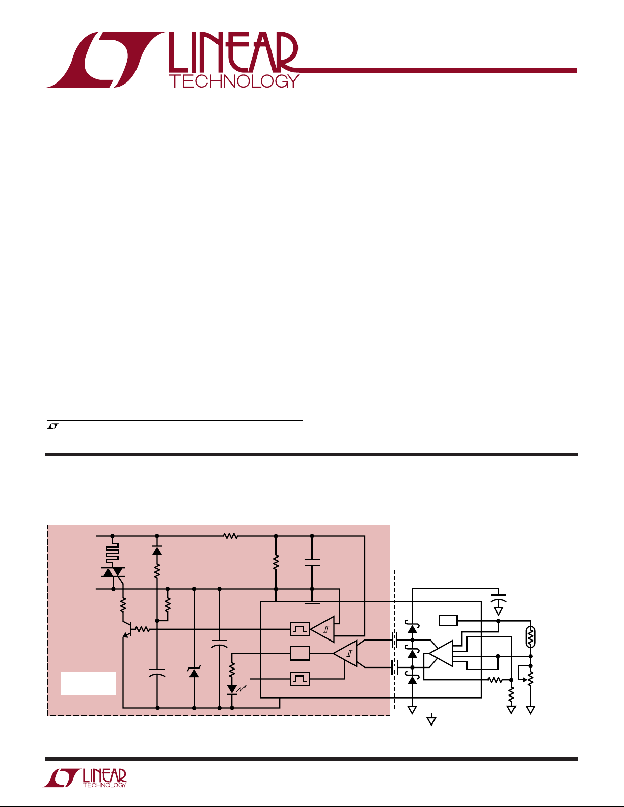
The LTC®1531 is an isolated self-powered dual differential
comparator. An internal capacitive isolation barrier provides 2500V
its output. The part provides UL-rated isolated comparisons without the need for an isolated supply since both
comparator power and output data are transmitted across
the capacitive barrier. The comparator data is transferred
differentially across the isolation barrier to provide high
common mode voltage and noise immunity.
of isolation between the comparator and
RMS
■
Self-Powered Isolated Sensing
■
Isolated Temperature Control
■
Isolated Voltage Monitor
■
Isolated Switch Control
, LTC and LT are registered trademarks of Linear Technology Corporation.
U
TYPICAL APPLICATION
Isolated Thermistor Temperature Controller
AC
120V
TECCOR
Q4008L4
OR EQUIVALENT
NEUTRAL
DANGER!
LETHAL VOLTAGES
IN THIS SECTION!
2N2222
LOAD
25Ω
150Ω
1k
–5.6V
1N4004
3k
3W
750Ω
0.5W
+
20µF
50V
5.6V
R1
680k
+
100µF
390Ω
LED
V
CC
ZCDATA
DATA
VALID
GND
R2
47k
The isolated side can supply a 2.5V reference output to
power external sensor circuits such as a thermistor bridge.
The dual differential comparator inputs allow for comparison of two differential voltages as well as single-ended
voltages. The powered side provides a latched data output
as well as a pulsed zero-cross comparator output for
controlling a triac. The part is available in a 28-lead SO
package.
C1
SHDN
QD
0.01µF
ZCPOS
LTC1531
ZCNEG
ISOLATION
BARRIER
V
PW
ISOGND
1
*HYSTERESIS = 1°C AT T
V
REG
2.5V
V1
V2
+
V3
–
V4
CMPOUT
R5*1M
= ISOLATED GROUND
1
R
+
R
1µF
B = 3807
T
1
O
T
R6
22k
1
O
=
THERM
B (1/T – 1/TO)
O • e
= 297°K
THERM
30k
YSI 44008
R4
50k
1
1531 TA01
1
Page 2

LTC1531
WW
W
U
ABSOLUTE MAXIMUM RATINGS
(Note 1)
Total Supply Voltage (VCC to GND) ............................ 7V
Input Voltages
Isolated Comparator
(V1 to V4).............................. –0.3V to (VPW + 0.3V)
SHDN, ZCPOS, ZCNEG ......................... –0.3V to 12V
Current
Input Pins .......................................................±10mA
ZCDATA, VALID, DATA .................................. ±10mA
Operating Temperature Range ..................... 0°C to 70°C
Storage Temperature Range ................. –65°C to 150°C
Lead Temperature (Soldering, 10 sec)..................300°C
U
W
PACKAGE/ORDER INFORMATION
TOP VIEW
V
1
CC
SHDN
2
ZCNEG
3
ZCPOS
4
11
V
PW
CMPOUT
Consult factory for Industrial and Military grade parts.
12
13
V
REG
14
ISOGND
28-LEAD PLASTIC SO (ISO)
T
= 125°C, θJA = 125°C/W
JMAX
SW PACKAGE
28
27
26
25
18
17
16
15
GND
ZCDATA
DATA
VALID
V1
V2
V3
V4
ORDER PART
NUMBER
LTC1531CSW
U
ELECTRICAL CHARACTERISTICS
The ● denotes specifications which apply over the full operating temperature range, otherwise specifications are TA = 25°C, VCC = 5V.
SYMBOL PARAMETER CONDITIONS MIN TYP MAX UNITS
I
VCC
V
ZCOS
V
HYS
f
SAMPLE
V
OS
R
VIN
I
VIN
V
REG
R
VREG
I
CMPOUT
t
VREG
V
PWH
I
VPW
V
ISO
Supply Current SHDN = VCC, No Load ● 10 14 mA
SHDN = 0V
Zero-Cross Offset VCM = V
Zero-Cross Hysteresis VCM = VCC (Note 7) ● 200 800 mV
Isolated Comparator Sample Rate V
Isolated Comparator Offset V1 = V2, V3 = V4 ● 2.0 4.0 mV
Isolated Comparator V1 = V3 = 2.5V, V2 = V4 = 0V 18 MΩ
Input Impedance V1 = V2 = 1.25V, V3 = V4 = 0V 300 MΩ
Isolated Comparator Input Current V1 = V3 – 2.5V, V2 = V4 = 0V ±1nA
V
REG
V
Output Impedance 2mA to 5mA Load ● 415 Ω
REG
CMPOUT High Impedance Leakage Current V
V
On-Time ● 90 108 130 µs
REG
VPW, Power Detect Enable Voltage 3.3 V
Current Transfer to V
Isolation Voltage 1 Minute (Note 6) ● 2500 V
PW
CC
Not Loaded (Note 2) 300 Hz
REG
V1 – V3 = 2V, V4 – V2 = 2V
f
= 700Hz (Note 4)
SAMPLE
2mA Load VPW = 3.3V (Note 5) ● 2.40 2.50 2.55 V
= 2.5V 1 nA
CMPOUT
VPW = 0V 45 µA
V
= 3.3V 30 µA
PW
1 Second ● 4500 V
● 0.2 10 µA
● ±30 ±120 mV
● 2.0 4.0 mV
RMS
DC
2
Page 3
LTC1531
ELECTRICAL CHARACTERISTICS
The ● denotes specifications which apply over the full operating temperature range, otherwise specifications are TA = 25°C, VCC = 5V.
SYMBOL PARAMETER CONDITIONS MIN TYP MAX UNITS
V
IH
V
IL
V
OH
V
OL
I
, I
INL
INH
dV/dt Continuous dV/dt Rejection (Note 8) ● 50 70 V/µs
C
ISO
SHDN Input High Voltage VCC = 4.5V ● 2.4 V
SHDN Input Low Voltage VCC = 5.5V ● 0.8 V
DATA, VALID, ZCDATA Output High Voltage VCC = 4.5V, IO = –400µA ● 3.0 4.3 V
DATA, VALID, ZCDATA Output Low Voltage VCC = 4.5V, IO = 1.6mA ● 0.2 0.4 V
SHDN Low or High Level Input Current VIN = 5V, 0V ● ±1 µA
2pF
Note 1: Absolute Maximum Ratings are those values beyond which the life
of a device may be impaired.
Note 2: The sample rate is not continuous, but depends on V
charging
PW
rate. See Applications Information.
Note 3: See Applications Information for further description of the
comparator switched-capacitor input circuit.
Note 4: The sample rate, f
Note 5: Load on CMPOUT pulls current from V
Note 6: Value derived from 1 second test.
Note 7: Zero-cross hysteresis is the minimum amount of signal amplitude
above or below 0V differential to retrigger the zero-cross comparator.
Note 8: Parameter not tested but guaranteed by design.
UW
TYPICAL PERFORMANCE CHARACTERISTICS
V
RIPPLE
t
SAMPLE
V
REG
(V)
PW
V
3.3
2.5
VCC = 5V
= 1µF
C
VPW
= 5mA
I
VREG
= 25°C
T
A
V
PW
(V)
REG
V
3.3
2.5
SAMPLE
VCC = 5V, C
I
VREG
VPW
= 100µA, TA = 25°C
, varies with loading on VPW and V
when CMPOUT is high.
REG
= 1µF
REG
.
0
NOTES: V
t
RIPPLE
SAMPLE
100
TIME (ms)
DEPENDS ON C
DEPENDS ON I
Figure 1. VPW Power-Up and
V
Samples vs Time
REG
200 300
AND I
VPW
VPW
+ I
VREG
VPW
+ I
VREG
1531 F01
0
0
NOTE: NONPERIODIC SAMPLES DUE TO DEPENDENCE
ON V
SAMPLING
PW
Figure 2. V
(I
VREG
2010
TIME (ms)
> 3.3V AND THE POWER-LISTEN CYCLE
REG
30 40
1531 F02
and VPW vs Time
= 100µA)
3
Page 4
LTC1531
UW
TYPICAL PERFORMANCE CHARACTERISTICS
30
TA = 25°C
25
20
(ms)
15
SAMPLE
t
10
5
0
0
Figure 3. Average t
VCC = 4.5V
VCC = 5.5V
VCC = 5V
I
VREG
2
(mA)
SAMPLE
1
3
vs I
4
1531 F03
VREG
UUU
PIN FUNCTIONS
VCC (Pin 1): Powered Side Power Supply.
SHDN (Pin 2): Active Low Chip Shutdown. A low signal
causes the circuitry to power down. DATA logic output
level will be reset to zero during power-down.
ZCNEG (Pin 3): Zero-Cross Comparator Negative Input.
ZCPOS (Pin 4): Zero-Cross Comparator Positive Input.
VPW (Pin 11): Isolated Power Supply. Connect to an
external storage capacitor.
4500V
BREAKDOWN
LIMIT
RMS
V
10k 10M
100k 1M 100M
FREQUENCY (Hz)
Figure 4. V
2500V
450V
45V
vs Frequency
RMS
RMS
SLEW RATE = (π)(f)(V
= (1.11)(f)(V
50V/µs
(1.11)(f)
4.5V
450mV
1531 F04
= V
RMS
P-P
)
RMS)
equal to (V1 + V2)/2 > (V3 + V4)/2 or equivalently (V1 – V3)
> (V4 – V2).
V3 (Pin 16): Comparator Negative Input.
V2 (Pin 17): Comparator Positive Input.
V1 (Pin 18): Comparator Positive Input.
VALID (Pin 25): Pulsed Output. Indicates when valid data
was received from the comparator. May be used to clock
DATA to external circuitry.
CMPOUT (Pin 12): Isolated Latched Comparator Data.
CMPOUT is active when V
is on. The CMPOUT output
REG
can be used on the isolated side for hysteresis (see
applications). The output will contain the result of the
previous comparison. When V
is low, the CMPOUT pin
REG
is Hi-Z.
V
(Pin 13): Isolated 2.5V Regulated Output. Pulsed on
REG
for 100µs with a maximum load current of 5mA. V
REG
also
supplies power to the CMPOUT output (Pin 12).
ISOGND (Pin 14): Isolated Side Power Ground.
V4 (Pin 15): Comparator Negative Input. The comparator
inputs are summed together with the comparison output
4
DATA (Pin 26): Latched Comparator Result. DATA holds
the value of the last valid comparison result. DATA changes
only when a valid comparison was received from the
isolated side.
ZCDATA (Pin 27): A 24µs to 30µs Pulsed Output. The
pulse occurs when the DATA output is high and the zerocross comparator inputs (ZCPLS-ZCNEG) cross zero volts
differential. Typically the zero-cross input signal is an RC
phase shifted AC sine wave. This output is a TTL level pulse
that can be used for firing an external triac.
GND (Pin 28): Power Supply Low Impedance Ground
Connection.
Page 5
UWW
TI I G DIAGRA
LTC1531
V
REG
CMPOUT
VALID
DATA
BLOCK DIAGRAM
W
POWER CYCLE
960µs
POWER
Hi-Z
POWER-LISTEN CYCLE
1152µs
ISOLATION
BARRIER
LISTEN CYCLE
192µs
LISTEN
108µs
200ns
1531 TD01
V
VALID
DATA
ZCDATA
GND
POWERED SIDE
V
CC
1
CC
25
TIMING
VOLTAGE
PUMP
V
PW
11
3.3V
DET
TRANSMIT
AND
DRIVER
+
Q
26
27
28
D
R
ZERO-CROSS
COMPARATOR
DECODE
POWER-ON
RESET
–
4
ZCPOS ZCNEG SHDN
2
3
14
ISOGND
TIMING
ISOLATED SIDE
LATCH
2.5V
REG
COMPARE
V1
18
V2
+
–
17
Σ
V3
16
Σ
V4
15
V
REG
13
CMPOUT
12
1531 BD
5
Page 6

LTC1531
U
WUU
APPLICATIONS INFORMATION
The LTC1531 is an isolated self-powered dual differential
comparator. It contains a switched-capacitor comparator
that is self-powered through a capacitive isolation barrier.
The capacitive isolation barrier provides 2500V
isolation. The isolated comparator cycles between storing
power and performing sampled comparisons. During the
power delivery cycle, the nonisolated powered side delivers power through the internal isolation capacitors and
rectifier onto an external storage capacitor. Periodically
the isolated comparator makes a comparison if sufficient
voltage has been stored on the external supply capacitor.
See Timing and Block Diagrams.
During a comparison, the isolated side uses the energy
stored on the external capacitor to deliver a regulated 2.5V
power source for 108µs followed by a sampled compari-
son. The result is transmitted back to the nonisolated
powered side and latched as the logic level DATA output.
A comparison will occur during the listen cycle if sufficient
voltage (3.3V) has been stored on the isolated external
capacitor. New DATA is latched only if a comparison was
actually done. A zero-crossing trigger pulse output for
firing a triac, ZCDATA, is available to trigger a triac when
the latched DATA output is high. A VALID data output pulse
is provided after each power-listen cycle in which a comparison was done to indicate that DATA has been updated.
The VALID output can be used to clock external circuitry
when a new comparator DATA value occurs.
POWER-LISTEN CYCLE
Self-Powering Through the Isolation Barrier
The LTC1531 comparator powered side toggles between
delivering power to the isolated side and listening for a
comparison result (see Timing Diagram). During the power
cycle, AC power is delivered through the isolation capacitors, formed in the lead frame, to the isolated side. During
the listen cycle, the powered side receives pulses from the
isolated side and determines if a valid comparison
occurred.
The isolated side of the LTC1531 requires an external
capacitor connected to VPW whose value must be large
enough to sustain less than a 300mV drop for 108µs with
the internal + external V
load current. Power is deliv-
REG
RMS
of
ered to this external capacitor through the internal isolation capacitors and rectifiers during the power cycle.
When this voltage reaches approximately 3.3V, the compare circuitry is enabled and a comparison will occur
during the next listen cycle. With VCC = 5V, this capacitive
coupled isolated power source can be modeled as an
equivalent 5.3V to 6.5V source with a 100kΩ source
impedance. The VPW pin will tend to self-regulate at 3.3V
with a ripple determined by the discharge current supplied
during the 108µs V
capacitor value. The value of the capacitor affects the initial
start-up time and the ripple voltage on VPW, but it does not
influence the sample rate of the comparator. This is
because the sample rate is determined by the rate of power
delivered through the isolation barrier and the rate it is
consumed in the internal plus external isolated circuits.
Any excessive external DC loading on VPW may prevent the
capacitor voltage from reaching the required 3.3V enable
voltage. Up to 20µA of continuous loading on VPW can be
tolerated based on the 100k, 5.3V model of the power
source (see Typical Applications for examples). The quiescent current of the isolated side is approximately 2µA
to 3µA.
SAMPLE RATE
The comparator sample rate depends on the charging rate
through the isolated capacitors and the external + internal
load current . The power-listen cycles at 700Hz to 900Hz,
however, a comparison will only occur when VPW exceeds
the 3.3V enable voltage. Typical sample rate for light
loading is 200Hz to 300Hz. The actual sampling is not
uniform, but occurs during the listen period of the power
cycle and when VPW ≥ 3.3V. Typical sample rates for
various supply and load conditions are plotted in Figure 3.
Continuous micropower loads will also decrease the sample
rate.
V
Reference Output
REG
The V
108µs at 2.5V. During the off time, V
impedance. The V
Large capacitance should not be attached to V
to avoid power loss. Charging of the V
reference output pulses on for approximately
REG
output pulse and the external
REG
does not go high
REG
output stage is shown in Figure 5.
REG
in order
REG
output capaci-
REG
6
Page 7

LTC1531
U
WUU
APPLICATIONS INFORMATION
V
PW
21k
2k
16k
1
ISOGND
V
GP
Figure 5. V
REG
V
PW
23k
16k
1
ISOGND
Output Stage
V
REG
1531 F05
V3 ≠ V4, the input impedance due to leakage currents is
about 15MΩ to 20MΩ. Since the comparator is turned on
only for the last 10µs of the 108µs V
period, the charge
REG
injection occurs at about the 98µs point with a coupling
capacitance of 2pF per input.
The CMPOUT signal is typically used to provide hysteresis, as in the Isolated Temperature Control application.
CMPOUT is the latched result of the previous comparison
and is active during the following V
is powered by V
, the internal 2.5V regulated output,
REG
ON period. CMPOUT
REG
and is in high impedance except during the 108µs
V
ON time. When active, CMPOUT is switched low to
REG
ISOGND or high to V
depending on the stored result of
REG
the previous comparison. The stored CMPOUT data is
reset during power-up. CMPOUT is not necessarily reset
by the powered side SHDN pin, except when shutdown
results in VPW drooping low enough to trigger a power-on
reset on the isolated side between 1.5V to 2.5V.
tance, which will subsequently be discharged between
samples, will consume power from VPW.
ISOLATED COMPARATOR INPUTS AND CMPOUT
The LTC1531 isolated comparator has a 4-input
summing comparator that performs the following
comparison:
(V1 + V2)/2 > (V3 + V4)/2
By rearranging the equation, for example, a dual differential comparison is performed:
(V1 – V4) > (V3 – V2) or (V1 – V3) > (V4 – V2)
The input has a rail-to-rail input and common mode
voltage range of VPW-ISOGND. The summing nature of the
inputs allows midsupply referencing. For example, connecting V3 to V
provide V
REG
and V4 to ISOGND sums together to
REG
/2 for the negative comparator input. See for
example, the Isolated Switch Control.
Charge injection and leakage currents occur at the com-
parator inputs. The amount depends on how the comparator is used. Minimum leakage currents occur with V1 = V2
and V3 = V4 where the input impedance is from charge
injection and is nominally 300MΩ. When V1 ≠ V2 or
DATA, VALID, ZCDATA
During a power cycle, the VALID signal goes high if a valid
comparison was made during the previous listen cycle.
VALID goes low at the beginning of the next listen cycle.
The low-to-high transition of VALID can be used to clock
DATA into external circuitry. VALID is delayed 200ns after
the DATA output. In order for a comparison to occur,
sufficient power must be stored on the isolated side
storage capacitor.
The DATA output holds the last received compare result.
DATA is reset to zero on power-up and shutdown. The
VALID output is held high for one power cycle following a
correctly received compare result. The received DATA
value from the isolated side contains redundancy to improve noise immunity.
The ZCDATA is a 25µs output pulse triggered by the zero-
cross comparator. In order for a pulse to occur, the DATA
output must be at logic 1 and the ZCPOS-ZCNEG zerocross comparator input crosses 0V after the input has
exceeded the ±150mV to 800mV of hysteresis. The zerocross comparator output is typically used to trigger a triac
from a 60Hz RC phase shifted AC line signal. See Typical
Applications.
7
Page 8

LTC1531
U
WUU
APPLICATIONS INFORMATION
The zero-cross comparator inputs, ZCPOS and ZCNEG,
have an input common mode range that allows signal
swings near the positive supply rails. The ZCPOS and
ZCNEG inputs contain ESD diode protection devices which
will clamp input signals that go below GND. The current
into the diode should be limited to less than 5mA. The
Isolated Thermistor Temperature Controller shows an
example phase shift network with attenuation that satisfies these conditions. The positive input voltage should
not exceed the 12V maximum rating or the 5mA input
current to the ESD diode clamp.
ISOLATION dV/dt
The maximum continuous dV/dt across the isolation barrier that will still allow the isolated comparator to operate
is 50V/µs. Continuous rates of dV/dt greater than this
cause the isolated side to not detect when its power cycle
has stopped and a comparison should begin. Figure 4
shows the maximum continuous rate trade-off of frequency vs voltage of a sine wave:
TOP VIEW
V
1
CC
SHDN
2
ZCNEG
3
ZCPOS
4
11
V
PW
CMPOUT
Figure 6. PC Board Layout Consideration
12
13
V
REG
14
ISOGND
28-LEAD PLASTIC SO (ISO)
SW PACKAGE
28
GND
27
ZCDATA
26
DATA
25
VALID
ETCH COPPER
FROM THE
SHADED AREA
18
V1
17
V2
16
V3
15
V4
TYPICAL APPLICATIONS DESCRIPTION
1531 F06
SR = (π)(f)(V
where SR = slew rate, V
P-P
)
= the peak-to-peak voltage and
P-P
f = frequency. Noise immunity to intermittent dV/dt rates
greater than 50V/µs can be rejected by the LTC1531.
AC Noise Rejection and Things to Avoid
Minimizing AC noise pickup at the isolated comparator
should follow the following guidelines.
1. Allow the isolated side ground to float. The isolated side
should only be common with the isolated circuit.
2. Use hysteresis to decrease sensitivity by using CMPOUT.
3. Use lower impedance circuits if powered by V
Avoid large capacitance tied directly to V
REG
output,
REG
.
since this output does not go Hi-Z (high impedance)
during the off time.
PC Board Layout
The PC board layout should not have copper near the lead
frame isolation capacitors. The copper reduces the power
coupling and power delivery to the isolated side (see
Figure 6).
The Isolated Thermistor Temperature Controller (front
page) uses a simple AC power rectifier and Zener to
provide 5.6V of DC power to the LTC1531. To avoid power
dissipation in the 3k, 3W resistor, DC power can be
provided with a charge pump circuit similar to the Isolated
Switch Control. In this circuit, a thermistor half bridge is
used with the 4-input comparator connected to provide
the other half of the bridge, V4 = 2.5V, V3 = 0V, giving
(V4 + V3)/2 = 1.25V. With the 50k pot set to about 30k, the
trip point is 25°C with a hysteresis of ±0.5°C. Here, V
REG
turns on and powers the half-bridge while the comparator
samples the result. The zero-cross comparator, ZCPOS
and ZCNEG, is used to trigger a triac at the 10° phase point.
The circuit, R1, R2 and C1, provides the phase shift, θ, as
determined by:
R2C1 ≅ tan(θ)/2π60Hz
and where the attenuation ≅ R2/R1. In this example,
R1 = 680k, R2 = 47k and C1 = 0.01µF, provide a 7V peak
input signal with 10° of phase lag.
8
Page 9

LTC1531
U
WUU
APPLICATIONS INFORMATION
The Remote Light-Controlled Switch (Figure 7) is similar
to the Isolated Thermistor Temperature Controller. The
thermistor is replaced with a Cadmium Light Sensor.
The Isolated Switch Control (Figure 8) is also similar,
where a low voltage switch is isolated from the AC power
control. Here, a charge pump using the 1µF nonpolar
capacitor and diodes are used for powering the LTC1531.
The Isolated Voltage Sense circuit (Figure 9) uses the
three-state CMPOUT pin in a delta-sigma configuration.
Here, the time constant of R1C1 is increased by the
effective duty cycle of CMPOUT ON to OFF time. At a 300Hz
sample rate and a typical ON time of 108µs, the time
constant is:
(1M • 0.22µF)/(300Hz • 108µs) ≈ 6.6sec
The input range is 0V to 2.5V set by the V
voltage. The output is recovered using a rail-to-rail op
amp, LT1490, averaging circuit with a 10sec time constant. The output range is 0V to VCC output for a 0V to V
input range.
The Isolated Potentiometer Transducer Sense circuit
(Figure 10) uses the same principle as the Isolated Voltage
Sense circuit to provide a 0V to VCC output proportional to
the potentiometer sensor input.
The Isolated Thermocouple Voltage circuit (Figure 11)
again uses the delta-sigma approach to translate a thermocouple temperature into a 0V to VCC output. Additionally, a micropower op amp, the LT1495, is used to provide
a continuous voltage amplification of the thermocouple.
The LT1389 with the thermistor bridge provides cold
junction compensation over a 0°C to 60°C temperature
range within ±0.5°C. The op amp gain is set to give the Ktype thermocouple a 0°C to 200°C range which translates
to a 0V to VCC output signal. Reducing R3 will increase the
temperature sensing range.
The Over Temperature Detect circuit (Figure 12) uses the
same continuous micropower cold junction compensation circuit as in the Isolated Thermocouple Voltage circuit. In this case, the comparator’s minus input is set to
1.25V, which corresponds to 100°C as set by the LT1495
REG
output
REG
op amp gain. When the thermocouple exceeds 100°C,
V
goes high.
TRIP
The Isolated Battery Cell Monitor circuit (Figure 13) uses
LTC1531 isolation to both float the individual grounds on
the isolated comparator and isolate the battery from the
logic outputs, CELL1, CELL2, ... In this application, R1 and
R2 (R3 and R4) divide the 2.5V reference down to 0.89V,
while the cell voltage is divided in half by connecting V1 to
the cell and V2 to 0V. Hence, when the cell voltage drops
below 1.786V, CELL1 goes high. Likewise for additional
cells with additional LTC1531s.
The Isolated Window Comparator circuit (Figure 14) uses
two LTC1531s and a logic gate to provide isolated window
comparisons. In this circuit, the first LTC1531, V
HIGH
,
does the comparison:
V1 – V3 > V4 – V2
or
–
(0V – X • V
REG
) > (V
IN
– V
IN
+
)
or
X • V
REG
< (V
IN
+
– V
IN
–
)
where X = R2/(R2 + R1).
The second LTC1531, V
(–X • V
When (V
IN
REG
+
– V
and when (V
) > (V
IN
+
IN
–
) is less than –X • V
IN
+
– V
IN
goes high. In between –X • V
is high. Therefore, the window width is 2 • X • V
, does the comparison:
LOW
–
– V
)
IN
, V
REG
–
) is greater than X • V
and +X • V
REG
LOW
REG
goes high
, V
REG
HIGH
, V
WINDOW
.
REG
The AC Line Overcurrent Detect circuit (Figure 15) uses
the micropower op amps, the quad LTC1496, to peak
detect the voltage across a sense resistor in series with an
AC load. The two amplifiers connected to R
SENSE
act as
half-wave rectifiers because their outputs cannot swing
below ground. The gain is set to trip when the voltage on
R
exceeds 125mV and the minus comparator input
SENSE
is set to 1.25V. The peak detector has a discharge resistor
of 1M plus the op amp input bias current.
9
Page 10

LTC1531
TYPICAL APPLICATIONS
AC
120V
TECCOR
Q4008L4
OR EQUIVALENT
NEUTRAL
DANGER!
LETHAL VOLTAGES
IN THIS SECTION!
2N2222
LOAD
25Ω
150Ω
1N4004
3k
3W
750Ω
0.5W
1k
+
20µF
50V
U
5.6V
R1
680k
V
CC
ZCDATA
DATA
R2
47k
+
100µF
VALID
GND
SHDN
QD
C1
0.01µF
LTC1531
ISOLATION
BARRIER
ZCPOS ZCNEG
TRIAC FIRING:
θ = DESIRED PHASE LAG
R2 • C1 = Tan(θ)/(2π60Hz)
R2/(R1 + R2) = ATTENUATION
V
PW
2.5V
+
–
CMPOUT
ISOGND
1
= ISOLATED GROUND
1
V
REG
V1
V2
V3
V4
+
2.2µF
1
1
HYSTERESIS
560k
CADMIUM
LIGHT
SENSOR
100k
100k
1531 F07
1
AC
120V
TECCOR
Q4008L4
OR EQUIVALENT
NEUTRAL
DANGER!
LETHAL VOLTAGES
IN THIS SECTION!
150Ω
2N2222
LOAD
25Ω
10µF
50V
Figure 7. Remote Light-Controlled Switch
1N4004
5.6V
+
R1
680k
390Ω
100µF
LED
V
CC
ZCDATA
DATA
VALID
GND
R2
47k
SHDN
QD
C1
0.01µF
LTC1531
ZCPOS ZCNEG
ISOLATION
BARRIER
V
PW
ISOGND
1
TRIAC FIRING:
θ = DESIRED PHASE LAG
R2 • C1 = Tan(θ)/(2π60Hz)
R2/(R1 + R2) = ATTENUATION
+
1µF
V
REG
2.5V
+
–
CMPOUT
= ISOLATED GROUND
1
1
V1
V2
V3
V4
1M
1 1
LOW
VOLTAGE
SWITCH
1531 F08
1µF
275V
+
1k
470Ω
2W
10
Figure 8. Isolated Switch Control
Page 11

U
TYPICAL APPLICATIONS
R2
10M
C2, 1µF
V
V
OUT
0V TO V
CC
FULL-SCALE
OUTPUT
RESOLUTION = 4mV
SETTLING TIME = 10sec
CC
LT1490
R3
10M
–
V
+
LTC1531
V
CC
V
CC
ZCDATA
DATA
CC
10k
10k
VALID
GND
SHDN
QD
= ISOLATED GROUND
1
= EQUIPMENT GROUND
ZCPOS ZCNEG
LTC1531
ISOLATION
BARRIER
V
PW
ISOGND
1
DELTA-SIGMA TYPE MODULATION:
CMPOUT IS ON 108µs AT ~300Hz RATE
THEREFORE: 108µs • 300Hz = 1/30TH
TIME CONSTANT = 1M • 30 • 0.22µF = 6.6sec
2.5V
+
–
CMPOUT
V
REG
+
2.2µF
1
V1
V2
V3
V4
0V TO 2.5V
FULL-SCALE
INPUT
R1, 1M
C1
0.22µF
1
1531 F09
V
OUT
0V TO V
CC
FULL-SCALE
OUTPUT
RESOLUTION = 4mV
SETTLING TIME = 10sec
C2, 1µF
R2
10M
V
CC
LT1490
Figure 9. Isolated Voltage Sense
V
CC
V
CC
ZCDATA
R3
10M
–
V
CC
+
10k
10k
DATA
VALID
GND
SHDN
QD
= ISOLATED GROUND
1
= EQUIPMENT GROUND
ZCPOS ZCNEG
LTC1531
ISOLATION
BARRIER
V
PW
ISOGND
1
DELTA-SIGMA TYPE MODULATION:
CMPOUT IS ON 108µs AT ~300Hz RATE
THEREFORE: 108µs • 300Hz = 1/30TH
TIME CONSTANT = 1M • 30 • 0.22µF = 6.6sec
2.5V
+
–
CMPOUT
V
REG
+
2.2µF
1
V1
V2
V3
V4
100k
1
R1, 1M
C1
0.22µF
1
1531 TA05
Figure 10. Isolated Potentiometer Transducer Sense
11
Page 12

LTC1531
U
TYPICAL APPLICATIONS
V
TEMP
R2
10M
C2, 1µF
V
LT1490
V
PW
+
V
CC
V
ZCDATA
CC
10M
–
+
DATA
V
CC
VALID
10k
10k
SHDN
CC
QD
GND
V
OUTPUT = 0V TO V
TEMP
= 0°C TO 200°C
RESOLUTION = 0.4mV OR 0.5°C
RESPONSE TIME CONSTANT = 10sec
ZCPOS ZCNEG
LTC1531
CC
ISOLATION
BARRIER
V
PW
ISOGND
1
2.2µF
1
V
2.5V
+
–
REG
Σ
Σ
CMPOUT
= ISOLATED GROUND
1
= EQUIPMENT GROUND
V1
V2
V3
V4
R1
1M
1M
0.1µF
R3, 10M
LT1495
1
COLD JUNCTION COMPENSATES 0°C TO 60°C
C1
0.22µF
1
LT1389
1.74M
1
10.2k
33k
–
+
1.21k
V
THERM
30k
YSI44008
11.8k
1
PW
–
UNUSED OP AMP
LT1495
TIED FOR MIN
CURRENT DRAIN
+
1
1531 F11
–
K
+
Figure 11. Isolated Thermocouple Voltage
0.1µF
10M
LT1495
1
LT1495
1M
–
+
LT1389
1
33k
V
PW
–
UNUSED OP AMP
TIED FOR MIN
CURRENT DRAIN
+
1
10.2k
1.21k
1.74M
THERM
30k
YSI44008
11.8k
1
1531 F12
–
K
+
V
PW
+
2.5V
2.2µF
1
V
REG
V1
Σ
Σ
CMPOUT
V2
V3
V4
1
+
–
V
CC
V
ZCDATA
TRIP
DATA
VALID
V
SHDN
CC
QD
GND
= ISOLATED GROUND
1
= EQUIPMENT GROUND
LTC1531
ISOLATION
BARRIER
ZCPOS ZCNEG
V
PW
ISOGND
1
COLD JUNCTION COMPENSATES 0°C TO 60°C
VTRIP SWITCHES AT 100°C, SET BY OP AMP GAIN
Figure 12. Over Temperature Detect
12
Page 13

U
TYPICAL APPLICATIONS
5V
V
CC
ZCDATA
DATA
VALID
GND
V
CC
ZCDATA
DATA
VALID
GND
QD
QD
CELL 1
CELL 2
SHDN
SHDN
ZCPOS ZCNEG
LTC1531
ZCPOS
LTC1531
ISOLATION
BARRIER
ZCNEG
V
PW
ISOGND
V
PW
ISOGND
2.5V
2.5V
+
–
CMPOUT
+
–
CMPOUT
LTC1531
TRIP
TO
OTHER
CELLS
+
+
+
2.2µF
V
REG
V1
V2
V3
V4
R3
180k
R4
100k
+
2.2µF
V
REG
V1
V2
V3
V4
R1
180k
V
= 1.8V
R2
100k
Figure 13. Isolated Battery Cell Monitor
1531 F13
TO
OTHER
CELLS
13
Page 14

LTC1531
TYPICAL APPLICATIONS
5V
V
CC
ZCDATA
DATA
VALID
GND
V
CC
ZCDATA
DATA
VALID
GND
QD
QD
V
WINDOW
V
V
LOW
HIGH
U
SHDN
LTC1531 (2)
SHDN
LTC1531 (1)
= ISOLATED GROUND
1
= EQUIPMENT GROUND
ISOLATION
BARRIER
ZCPOS ZCNEG
ZCPOS ZCNEG
V
PW
2.5V
+
–
CMPOUT
ISOGND
1
V
PW
2.5V
+
–
CMPOUT
ISOGND
WINDOW WIDTH = 1V
1
R1 = R2 (5/WIDTH – 1)
+
2.2µF
V
REG
V1
V2
V3
V4
+
V
REG
V1
V2
V3
V4
2.2µF
+
V
IN
–
R1
400k
WIDTH/2
R2
100k
1531 F14
14
Figure 14. Isolated Window Comparator
Page 15

PACKAGE DESCRIPTION
28-Lead Plastic Small Outline Isolation Barrier (Wide 0.300)
U
Dimensions in inches (millimeters) unless otherwise noted.
SW Package
(LTC DWG # 05-08-1690)
0.697 – 0.712*
(17.70 – 18.08)
2526
2728
LTC1531
18
16 15
17
NOTE 1
23
0.050
(1.270)
BSC
1
0.291 – 0.299**
(7.391 – 7.595)
0.005
(0.127)
RAD MIN
0.009 – 0.013
(0.229 – 0.330)
NOTE:
1. PIN 1 IDENT, NOTCH ON TOP AND CAVITIES ON THE BOTTOM OF PACKAGES ARE THE MANUFACTURING OPTIONS
THE PART MAY BE SUPPLIED WITH OR WITHOUT ANY OF THE OPTIONS.
DIMENSION DOES NOT INCLUDE MOLD FLASH. MOLD FLASH SHALL NOT EXCEED 0.006" (0.152mm) PER SIDE
*
DIMENSION DOES NOT INCLUDE INTERLEAD FLASH. INTERLEAD FLASH SHALL NOT EXCEED 0.010" (0.254mm) PER SIDE
**
0.010 – 0.029
(0.254 – 0.737)
NOTE 1
0.016 – 0.050
(0.406 – 1.270)
× 45°
0° – 8° TYP
0.093 – 0.104
(2.362 – 2.642)
4
0.014 – 0.019
(0.356 – 0.482)
TYP
11 12
0.394 – 0.419
(10.007 – 10.643)
1413
0.037 – 0.045
(0.940 – 1.143)
0.004 – 0.012
(0.102 – 0.305)
SW28 (ISO) 1098
Information furnished by Linear Technology Corporation is believed to be accurate and reliable.
However, no responsibility is assumed for its use. Linear Technology Corporation makes no representation that the interconnection of its circuits as described herein will not infringe on existing patent rights.
15
Page 16

LTC1531
TYPICAL APPLICATION
ISOLATION
BARRIER
ZCDATA
V
DATA
TRIP
VALID
NEGATIVE COMPARATOR
INPUT SET TO 1.25V
R
SENSE
R
SENSE
V
CC
V
GND
= LIVE AC-CONNECTED
2
LOCAL CIRCUIT COMMON
= EQUIPMENT GROUND
SHDN
CC
Q
D
LTC1531
IN SERIES WITH AC LINE
TRIP VOLTAGE = 125mV
ZCPOS ZCNEG
U
V
PW
ISOGND
2
LETHAL VOLTAGES
IN THIS SECTION!
2.5V
+
–
CMPOUT
DANGER!
+
2.2µF
V
REG
V1
V2
V3
V4
1M
LT1496
2
1N4148
0.22µF
22
–
+
LT1496
V
PW
UNUSED OP AMP
TIED FOR MIN
CURRENT DRAIN
2
1M
51k
–
–
1M
LT1496
10k
+
+
1M
2
1M
LT1496
51k
–
10k
+
AC
R
SENSE
2
AC
Figure 15. AC Line Overcurrent Detect
RELATED PARTS
PART NUMBER DESCRIPTION COMMENTS
LTC1177 Isolated MOSFET Driver No Secondary Power Supply, 2500V
LT1389 Nanopower Reference 800nA, 0.05% Accuracy, 10ppm/°C Max Drift
LTC1440/LTC1441 Ultralow Power Single/Dual Comparators with Reference 2.1µA Typ, 2V to 11V Supply, Adjustable Hysteresis
LTC1442
LT1495/LT1496 1.5µA Max, Dual/Quad Precision Rail-to-Rail Input and Output Op Amps Low Offset 375µV
, 2.2V to 36V Supply
MAX
LTC1540 Nanopower Comparator with Reference 0.3µA Typ, Adjustable Hysteresis, 2V to 11V Supply
RMS
Isolation
1531 F15
16
Linear Technology Corporation
1630 McCarthy Blvd., Milpitas, CA 95035-7417
(408) 432-1900 ● FAX: (408) 434-0507
●
www.linear-tech.com
1531f, sn1531 LT/TP 0899 4K • PRINTED IN USA
LINEAR TECHNOLOGY CORPORATION 1998
 Loading...