

Page 1
FEATURES
■
High Power Buck Converter from 5V or 3.3V
Main Power
■
Adjustable Current Limit in S0-8 with
Topside FET R
■
No External Sense Resistor Required
■
Hiccup Mode Current Limit Protection
■
Adjustable, Fixed 1.9V, 2.5V, 2.8V and 3.3V Output
■
All N-Channel MOSFET Synchronous Driver
■
Excellent Output Regulation: ±2% over Line, Load
DS(ON)
Sensing
and Temperature Variations
■
High Efficiency: Over 95% Possible
■
Fast Transient Response
■
Fixed 300kHz Frequency Operation
■
Internal Soft-Start Circuit
■
Quiescent Current: 1mA, 45µA in Shutdown
U
APPLICATIO S
LTC1530
High Power Synchronous
Switching Regulator Controller
U
DESCRIPTIO
The LTC®1530 is a high power synchronous switching
regulator controller optimized for 5V to 1.3V-3.5V output
applications. Its synchronous switching architecture drives
two external N-channel MOSFET devices to provide high
efficiency. The LTC1530 contains a precision trimmed
reference and feedback system that provides worst-case
output voltage regulation of ±2% over temperature, load
current and line voltage shifts. Current limit circuitry
senses the output current through the on-resistance of
the topside N-channel MOSFET, providing an adjustable
current limit without requiring an external low value sense
resistor.
The LTC1530 includes a fixed frequency PWM oscillator
that free runs at 300kHz, providing greater than 90%
efficiency in converter designs from 1A to 20A of output
current. Shutdown mode drops the LTC1530 supply current to 45µA.
■
Power Supply for Pentium® II, AMD-K6®-2, SPARC,
ALPHA and PA-RISC Microprocessors
■
High Power 5V to 1.3V-3.5V Regulators
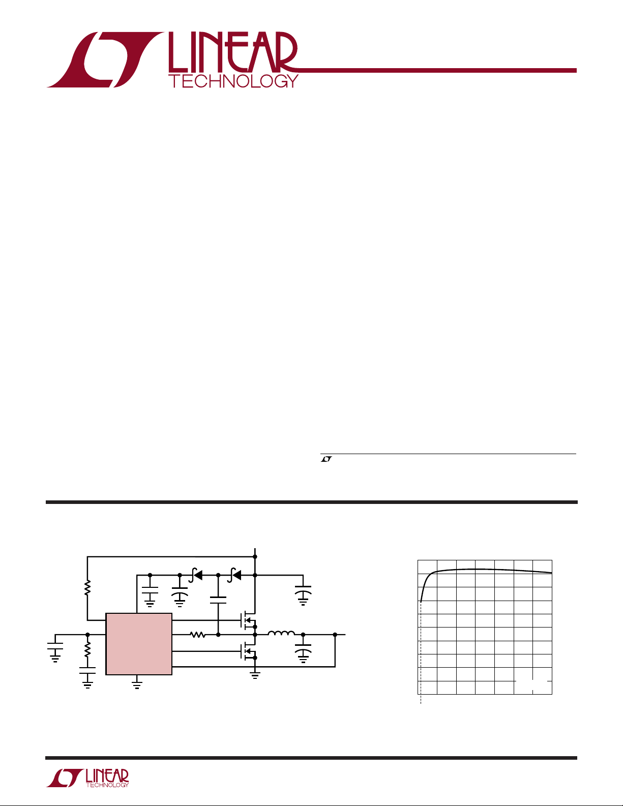
U
TYPICAL APPLICATIO
V
IN
5V
MBR0530T1 MBR0530T1
0.1µF
+
10µF
G1
I
G2
V
OUT
†
COILTRONICS CTX02-13198
OR PANASONIC ETQP6F2R5HA
††
AVX TPSE337M006R0100
20Ω
FB
0.22µF
Q1*
Q2*
COILTRONICS (561) 241-7876
C1
150pF
0.022µF
2.7k
PV
I
CC
MAX
COMP
R
LTC1530-3.3
C
10k
C
C
GND
Figure 1. Single 5V to 3.3V Supply
The LTC1530 is specified for commercial and industrial
temperature ranges and is available in the S0-8 package.
, LTC and LT are registered trademarks of Linear Technology Corporation.
Pentium is a registered trademark of Intel Corp.
AMD-K6 is a registered trademark of Advanced Micro Devices, Inc.
+
C
**
IN
1200µF
× 4
†
L
O
2µH
††
+
C
O
330µF
× 7
* SILICONIX SUD50N03-10
** SANYO 10MV1200GX
V
3.3V
14A
1530 F01a
OUT
Efficiency vs Load Current
100
90
80
70
60
50
40
EFFICIENCY (%)
30
20
10
0
0
2
0.3
4
LOAD CURRENT (A)
8
6
TA = 25°C
10
12
14
1530 F01b
1
Page 2
LTC1530
TOP VIEW
G1
G2
I
FB
I
MAX
PV
CC
GND
S8 PACKAGE
8-LEAD PLASTIC SO
1
2
3
4
8
7
6
5
*V
SENSE
/
V
OUT
COMP
WWWU
ABSOLUTE AXI U RATI GS
(Note 1)
Supply Voltage
PVCC........................................................................ 14V
Input Voltage
IFB (Note 2) ............................................... PVCC + 0.3V
I
........................................................ –0.3V to 14V
MAX
IFB Input Current (Notes 2,3) ............................–100mA
Operating Ambient Temperature Range
LTC1530C ............................................... 0°C to 70°C
LTC1530I............................................ –40°C to 85°C
Maximum Junction Temperature
LTC1530C, LTC1530I ...................................... 125°C
Storage Temperature Range ................. –65°C to 150°C
Lead Temperature (Soldering, 10 sec).................. 300°C
UU
W
PACKAGE/ORDER I FOR ATIO
ORDER PART
NUMBER
LTC1530CS8
LTC1530CS8-1.9
LTC1530CS8-2.5
LTC1530CS8-2.8
LTC1530CS8-3.3
LTC1530IS8
T
= 125°C, θJA = 130°C/W
JMAX
*V
FOR FIXED VOLTAGE VERSIONS
OUT
1530
153019
153028
153033
153025
S8 PART MARKING
LTC1530IS8-1.9
LTC1530IS8-2.5
LTC1530IS8-2.8
LTC1530IS8-3.3
1530I
530I19
530I28
530I33
530I25
Consult factory for Military grade parts.
ELECTRICAL CHARACTERISTICS
The ● denotes specifications that apply over the full operating temperature
range, otherwise specifications are at 0°C ≤ TA ≤ 70°C. PVCC = 12V unless otherwise noted. (Note 3)
SYMBOL PARAMETER CONDITIONS MIN TYP MAX UNITS
V
SENSE
V
OUT
g
mERR
Internal Feedback Voltage LTC1530CS8 (Note 4) 1.223 1.235 1.247 V
● 1.216 1.235 1.254 V
Output Voltage LTC1530CS8-1.9 (Note 4) 1.881 1.9 1.919 V
● 1.871 1.9 1.929 V
LTC1530CS8-2.5 (Note 4) 2.475 2.5 2.525 V
● 2.462 2.5 2.538 V
LTC1530CS8-2.8 (Note 4) 2.772 2.8 2.828 V
● 2.758 2.8 2.842 V
LTC1530CS8-3.3 (Note 4) 3.267 3.3 3.333 V
● 3.250 3.3 3.350 V
Error Amplifier Transconductance (Note 5) ● 1.6 2 2.6 millimho
The ● denotes specifications that apply over the full operating temperature range, otherwise specifications are at –40°C ≤ TA ≤ 85°C.
PVCC = 12V unless otherwise noted. (Note 3)
SYMBOL PARAMETER CONDITIONS MIN TYP MAX UNITS
PV
CC
V
UVLO
V
SENSE
2
Supply Voltage (Note 6) ● 13.2 V
Undervoltage Lockout Voltage (Note 7) 3.5 3.75 V
Internal Feedback Voltage LTC1530IS8 (Note 4) 1.223 1.235 1.247 V
● 1.210 1.235 1.260 V
Page 3
LTC1530
ELECTRICAL CHARACTERISTICS
The ● denotes specifications that apply over the full operating temperature
range, otherwise specifications are at –40°C ≤ TA ≤ 85°C. PVCC = 12V unless otherwise noted. (Note 3)
SYMBOL PARAMETER CONDITIONS MIN TYP MAX UNITS
V
OUT
∆V
I
PVCC
f
OSC
G
ERR
g
mERR
I
MAX
V
SHDN
SR
t
SS
tr, t
t
NOL
DC
OUT
SS
f
MAX
Output Voltage LTC1530IS8-1.9 (Note 4) 1.881 1.9 1.919 V
● 1.862 1.9 1.938 V
LTC1530IS8-2.5 (Note 4) 2.475 2.5 2.525 V
● 2.450 2.5 2.550 V
LTC1530IS8-2.8 (Note 4) 2.772 2.8 2.828 V
● 2.744 2.8 2.856 V
LTC1530IS8-3.3 (Note 4) 3.267 3.3 3.333 V
● 3.234 3.3 3.366 V
Output Load Regulation I
Output Line Regulation VIN = 4.75V to 5.25V, I
= 0 to 14A –5 mV
OUT
= 0 ±1mV
OUT
Operating Supply Current Figure 3, VFB = 0V (Note 8) 15 mA
Quiescent Current Figure 3, COMP = 0.5V, VFB = 5V ● 1.0 1.4 mA
Shutdown Supply Current Figure 3, COMP = 0 (Note 9) ● 45 80 µA
Internal Oscillator Frequency Figure 4 ● 250 300 350 kHz
Oscillator Valley Voltage V
Oscillator Peak Voltage V
at 0% Duty Cycle 2.5 V
COMP
at Max Duty Cycle 3.5 V
COMP
Error Amplifier Open-Loop DC Gain (Note 5) ● 40 54 dB
Error Amplifier Transconductance (Note 5) ● 1.6 2 2.8 millimho
I
Sink Current V
MAX
I
Sink Current Tempco V
MAX
= 5V 170 200 230 µA
IMAX
= 5V ● 120 200 300 µA
V
IMAX
= 5V 3300 ppm/°C
IMAX
Shutdown Threshold Voltage Figure 4, Measured at COMP Pin (Note 9) ● 100 180 mV
Internal Soft-Start Slew Rate Figure 4, COMP Pulls High, VFB = 0V 0.4 V/ms
(Notes 9, 10)
Internal Soft-Start Wake-Up Time Figure 4, COMP Pulls High to G1↑ (Note 10) 3.5 ms
Driver Rise and Fall Time Figure 4 ● 90 140 ns
Driver Nonoverlap Time Figure 4 ● 30 100 ns
Maximum G1 Duty Cycle Figure 4 ● 81 86 %
Note 1: Absolute Maximum Ratings are those values beyond which the life
of a device may be impaired.
Note 2: If I
is taken below GND, it is clamped by an internal diode. This
FB
pin handles input currents ≤ 100mA below GND without latch-up. In the
positive direction, it is not clamped to PVCC.
Note 3: All currents into device pins are positive; all currents out of device
pins are negative. All voltages are referenced to ground unless otherwise
specified.
Note 4: The LTC1530 is tested in an op amp feedback loop which
regulates V
SENSE
based on V
OUT
= 2V for the error amplifier.
COMP
or V
Note 5: The Open-loop DC gain and transconductance from the VFB pin to
the COMP pin are G
ERR
and g
versions, the actual open-loop DC gain and transconductance are G
and g
multiplied by the ratio 1.235/V
mERR
respectively. For fixed output voltage
mERR
.
OUT
ERR
Note 6: The total voltage from the PV
pin to the GND pin must be ≥8V
CC
for the current limit protection circuit to be active.
Note 7: G1 and G2 begin to switch once PV
is ≥ the undervoltage
CC
lockout threshold voltage.
Note 8: Supply current in normal operation is dominated by the current
needed to charge and discharge the external FET gates. This current varies
with the LTC1530 operating frequency, supply voltage and the external
FETs used.
Note 9: The LTC1530 enters shutdown if COMP is pulled low.
Note 10: Slew rate is measured at the COMP pin on the transition from
shutdown to active mode.
3
Page 4
LTC1530
UW
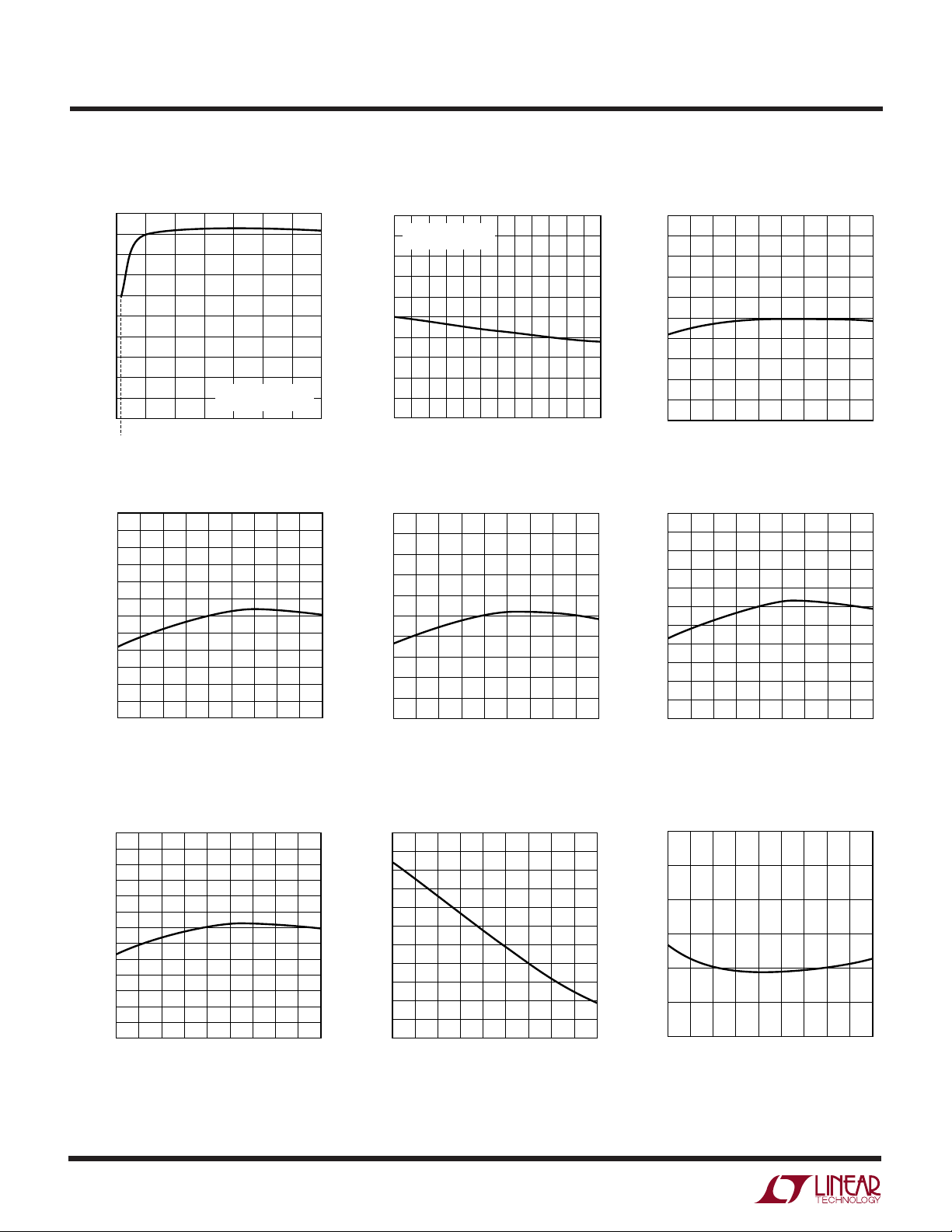
TYPICAL PERFOR A CE CHARACTERISTICS
Efficiency vs Load Current
100
90
80
70
60
50
40
EFFICIENCY (%)
30
20
10
0
0
0.3
4
2
LOAD CURRENT (A)
LTC1530-1.9 V
1.930
1.925
1.920
1.915
1.910
1.905
(V)
1.900
OUT
V
1.895
1.890
1.885
1.880
1.875
1.870
–55
–35
5
–15
TEMPERATURE (°C)
TA = 25°C
REFER TO FIGURE 10
8
6
OUT
25
10
vs Temperature
45 65 85 105 125
12
1530 G01
1530 G04
14
Load Regulation
2.510
TA = 25°C
2.508
REFER TO FIGURE 2
2.506
2.504
2.502
2.500
2.498
2.496
OUTPUT VOLTAGE (V)
2.494
2.492
2.490
0123456
OUTPUT CURRENT (A)
LTC1530-2.5 V
2.55
2.54
2.53
2.52
2.51
(V)
2.50
OUT
V
2.49
2.48
2.47
2.46
2.45
–35 5
–55
–15
TEMPERATURE (°C)
vs Temperature
OUT
85
45 125
25
65
1530 G02
105
1530 G05
LTC1530 V
1.260
1.255
1.250
1.245
1.240
(V)
1.235
SENSE
V
1.230
1.225
1.220
1.215
1.210
–55
LTC1530-2.8 V
2.85
2.84
2.83
2.82
2.81
2.80
(V)
OUT
2.79
V
2.78
2.77
2.76
2.75
2.74
–55
–15
–35 5
–35
–15
vs Temperature
SENSE
45 125
25
TEMPERATURE (°C)
5
TEMPERATURE (°C)
65
vs Temperature
OUT
25
45 65 85 105 125
85
105
1530 G03
1530 G06
4
(V)
OUT
V
3.36
3.35
3.34
3.33
3.32
3.31
3.30
3.29
3.28
3.27
3.26
3.25
3.24
3.23
LTC1530-3.3 V
–35
–55
–15
TEMPERATURE (°C)
vs Temperature
OUT
5
25
45 65 85 105 125
1530 G06
Undervoltage Lockout Threshold
Voltage vs Temperature
4.5
4.3
4.1
3.9
3.7
3.5
3.3
3.1
2.9
2.7
2.5
UNDERVOLTAGE LOCKOUT THRESHOLD (V)
2.3
–35 5
–55
–15
25
TEMPERATURE (°C)
45 125
65
Error Amplifier Transconductance
vs Temperature
2.8
2.6
2.4
2.2
2.0
1.8
1.6
ERROR AMPLIFIER TRANSCONDUCTANCE (millimho)
–35 5
–55
85
105
1530 G08
–15
25
TEMPERATURE (°C)
85
45 125
105
65
1530 G09
Page 5
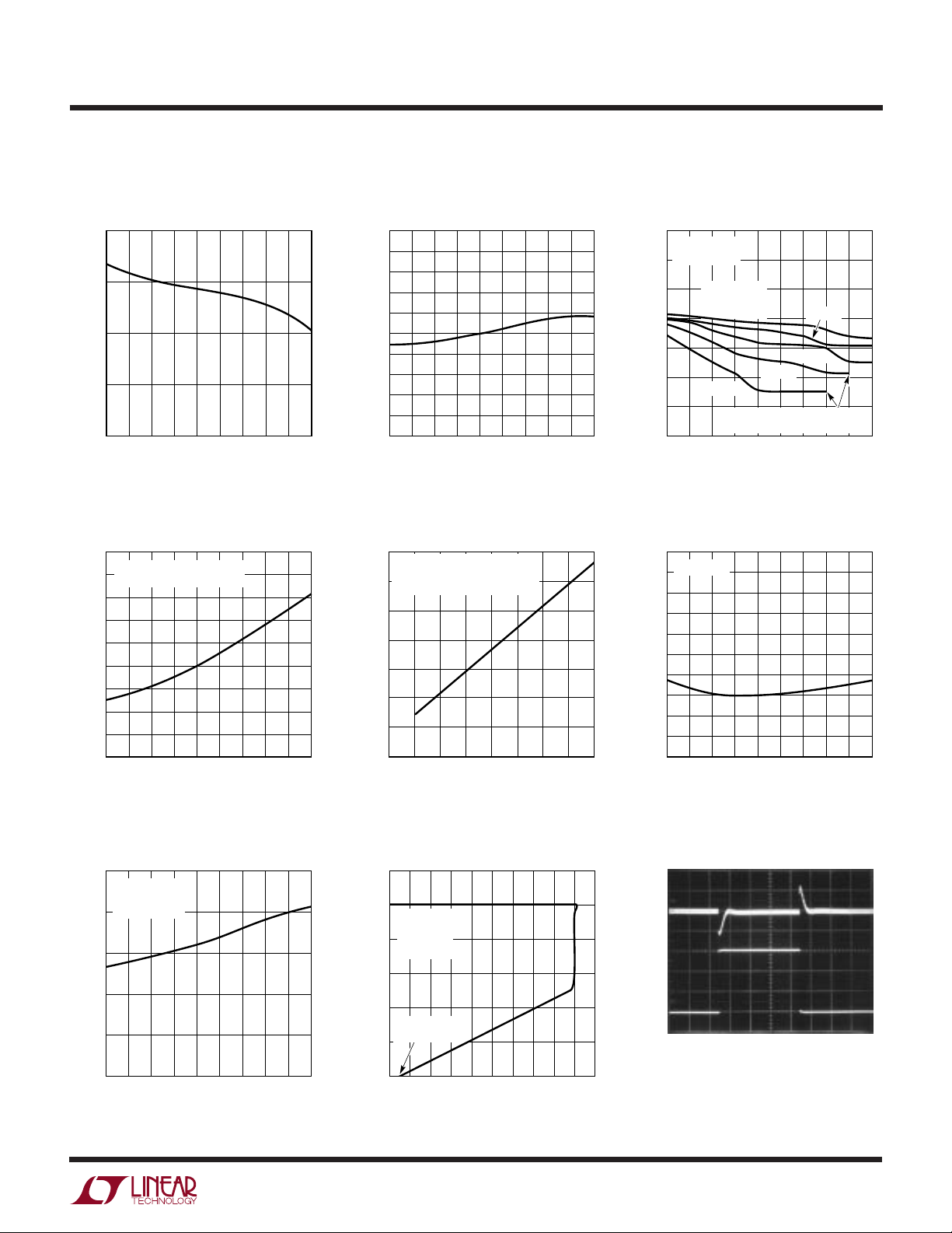
AMBIENT TEMPERATURE (°C)
–55
MAXIMUM G1 DUTY CYCLE (%)
92
90
88
86
84
82
80
78
–15
25
45 125
1530 G12
–35 5
65
85
105
THERMAL SHUTDOWN OCCURS
BEYOND THESE POINTS
G1, G2
CAPACITANCE
= 1000pF
PVCC = 12V
f
OSC
= 300kHz
7700pF
5500pF
3300pF
2200pF
TEMPERATURE (°C)
–55
80
75
70
65
60
55
50
45
40
35
30
–15
25
45 125
1530 G15
–35 5
65
85
105
PVCC = 12V
PV
CC
SHUTDOWN CURRENT (µA)
UW
TYPICAL PERFOR A CE CHARACTERISTICS
LTC1530
Error Amplifier Open-Loop Gain
vs Temperature
60
55
50
45
ERROR AMPLIFIER OPEN-LOOP DC GAIN (dB)
SINK CURRENT (µA)
MAX
I
40
300
280
260
240
220
200
180
160
140
120
–15
–35 5
–55
I
Sink Current vs Temperature
MAX
PVCC = 12V
G1, G2 ARE NOT SWITCHING
–15
–35 5
–55
25
TEMPERATURE (°C)
25
TEMPERATURE (°C)
85
45 125
65
85
45 125
65
105
105
1530 G10
1530 G13
Oscillator Frequency
vs Temperature
350
340
330
320
310
300
290
280
270
OSCILLATOR FREQUENCY (kHz)
260
250
–35 5
–55
–15
25
TEMPERATURE (°C)
PVCC Supply Current
vs Gate Capacitance
70
PVCC = 12V
= 25°C
T
A
60
GATE CAPACITANCE = C
50
40
30
SUPPLY CURRENT (mA)
20
CC
PV
10
0
1357
0
24 8
GATE CAPACITANCE (nF)
85
45 125
= C
G1
105
65
1530 G11
G2
6
1530 G14
Maximum G1 Duty Cycle
vs Ambient Temperature
PVCC Shutdown Supply Current
vs Temperature
Shutdown Threshold Voltage
vs Temperature Output Overcurrent Protection
250
PVCC = 12V
MEASURED AT
COMP PIN
200
150
100
50
SHUTDOWN THRESHOLD VOLTAGE (mV)
0
–35 5
–55
–15
TEMPERATURE (°C)
45 125
25
Transient Response
3.0
2.5
PVCC = 12V
T
= 25°C
A
2.0
REFER TO
FIGURE 2
1.5
1.0
OUTPUT VOLTAGE (V)
SHORT-CIRCUIT
CURRENT
0.5
85
105
65
1530 G16
0
213579
0
OUTPUT CURRENT (A)
6
4
8
1530 G17
50mV/DIV
2A/DIV
50µs/DIV 1530 G18
10
5
Page 6

LTC1530
U
UU
PI FU CTIO S
PVCC (Pin 1): Power Supply for G1, G2 and Logic. PV
must connect to a potential of at least VIN + V
GS(ON)Q1
VIN = 5V, generate PVCC using a simple charge pump
connected to the switching node between Q1 and Q2 (see
Figure 1) or connect PVCC to a 12V supply. Bypass PV
properly or erratic operation will result. A low ESR 10µF
capacitor or larger bypass capacitor along with a 0.1µF
surface mount ceramic capacitor in parallel is recommended from PVCC directly to GND to minimize switching
ripple. Switching ripple should be ≤100mV at the PV
pin.
GND (Pin 2): Power and Logic Ground. GND is connected
to the internal gate drive circuitry and the feedback circuitry. To obtain good output voltage regulation, use
proper ground techniques between the LTC1530 GND and
bottom-side FET source and the negative terminal of the
output capacitor. See the Applications Information section
for more details on PCB layout techniques.
V
SENSE/VOUT
(Pin 3): Feedback Voltage Pin. For the adjust-
able LTC1530, use an external resistor divider to set the
required output voltage. Connect the tap point of the
resistor divider network to V
and the top of the
SENSE
divider network to the output voltage. For fixed output
voltage versions of the LTC1530, the resistor divider is
internal and the top of the resistor divider network is
brought out to V
. In general, the resistor divider
OUT
network for each fixed output voltage version sinks approximately 30µA. Connect V
to the output voltage
OUT
either at the output capacitors or at the actual point of load.
V
SENSE/VOUT
is sensitive to switching noise injected into
the pin. Isolate high current switching traces from this pin
and its PCB trace.
COMP (Pin 4): External Compensation. The COMP pin is
connected to the error amplifier output and the input of the
PWM comparator. An RC + C network is typically used at
CC
. If
CC
CC
COMP to compensate the feedback loop for optimum
transient response. To shut down the LTC1530, pull this
pin below 0.1V with an open-collector or open-drain
transistor. Supply current is typically reduced to 45µA in
shutdown. An internal 4µA pullup ensures start-up.
I
(Pin 5): Current Limit Threshold. Current limit is set
MAX
by the voltage drop across an external resistor connected
between the drain of Q1 and I
pared with the voltage across the R
. This voltage is com-
MAX
of the high side
DS(ON)
MOSFET. The LTC1530 contains a 200µA internal pull-
down at I
to set current limit. This 200µA current
MAX
source has a positive temperature coefficient to provide
first order correction for the temperature coefficient of the
external N-channel MOSFET’s R
DS(ON)
.
IFB (Pin 6): Current Limit Sense Pin. Connect IFB to the
switching node between Q1’s source and Q2’s drain. If I
drops below I
with G1 on, the LTC1530 enters current
MAX
FB
limit. Under this condition, the internal soft-start capacitor
is discharged and COMP is pulled low slowly. Duty cycle
is reduced and output power is limited. The current limit
circuitry is only activated if PVCC ≥ 8V. This action eases
start-up considerations as PVCC is ramping up because
the MOSFET’s R
can be significantly higher than
DS(ON)
what is measured under normal operating conditions. The
current limit circuit is disabled by floating I
and short-
MAX
ing IFB to PVCC.
G2 (Pin 7): Gate Drive for the Low Side N-Channel MOSFET,
Q2. This output swings from PVCC to GND. It is always low
if G1 is high or if the output is disabled. To prevent
undershoot during a soft-start cycle, G2 is held low until
G1 first transitions high.
G1 (Pin 8): Gate Drive for the Topside N-Channel MOSFET,
Q1. This output swings from PVCC to GND. It is always low
if G2 is high or if the output is disabled.
6
Page 7
+
0.1µF
10µF
1530 F03
I
MAX
PV
CC
PV
CC
12V
GND
G1
NC
NC
NC
V
FB
I
FB
G2
V
SENSE/VOUT
COMPCOMP
LTC1530
BLOCK DIAGRA
LTC1530
W
COMP
–
+ 3%
LVC
MAX
DISDR
+
–
1
PV
CC
G1
8
G2
7
OUT
R1
23.4k
44.4k
54.9k
68.4k
R2
43.2k
43.2k
43.2k
40.8k
FIXED V
1.9V
2.5V
2.8V
3.3V
+
FB
FB
R2
V
V
/2
REF
REF
V
– 3%
REF
+ 3%
V
REF
/2
V
REF
R1
FOR FIXED
VOLTAGE
VERSIONS
3
V
SENSE
3
V
OUT
V
REF
1530 BD
LOGIC AND
INTERNAL
OSCILLATOR
I
COMP
4
I
C
SS
MHCL
SS
HCL
MONO
M
SS
g
= 2millimho
m
ERR MIN
+
–
V
REF
THERMAL SHUTDOWN
–
PWM
+
V
REF
–
CC
+
–
– 3%
I
MAX
+
POWER DOWN
I
6
FB
I
5
MAX
V
REF
TEST CIRCUITS
V
IN
5V
+
C
***
PV
CC
12V
750Ω
PV
CC
I
MAX
C1
100pF
0.01µF
R
8.2k
C
C
C
COMP
LTC1530-2.5
GND
G1
I
FB
G2
V
OUT
*SUMIDA CDRH127-2R4
**AVX TPSE337M006R0100
***SANYO 10MV1200GX
0.1µF
+
100Ω
Figure 2
10µF
Q1
Si4410DY
Q2
Si4410DY
L
O
2.4µH
*
IN
1200µF
× 2
V
OUT
CO**
+
330µF
× 8
2.5V
6A
1530 F02
Figure 3
7
Page 8
LTC1530
TEST CIRCUITS
PV
CC
12V
+
COMP
I
FB
COMP
V
OUT
PV
CC
LTC1530
GND
0.1µF
G1
3300pF
G2
3300pF
10µF
G1 RISE/FALL
G2 RISE/FALL
1530 F04a
WUUU
APPLICATIO S I FOR ATIO
t
r
90%
50%
10%
t
NOLtNOL
50%
Figure 4
90%
50%
10%
50%
t
f
COMP
G1
t
SS
1530 F04b
OVERVIEW
The LTC1530 is a voltage feedback, synchronous switching regulator controller (see Block Diagram) designed for
use in high power, low voltage step-down (buck) converters. It includes an on-chip soft-start capacitor, a PWM
generator, a precision reference trimmed to ±1%, two high
power MOSFET gate drivers and all the necessary feedback and control circuitry to form a complete switching
regulator circuit running at 300kHz.
The LTC1530 includes a current limit sensing circuit that
uses the topside external N-channel power MOSFET as a
current sensing element, eliminating the need for an
external sense resistor. If the current comparator, CC,
detects an overcurrent condition, the duty cycle is reduced
by discharging the internal soft-start capacitor through a
voltage-controlled current source. Under severe overloads or output short-circuit conditions, the soft-start
capacitor is pulled to ground and a start-up cycle is
initiated. If the short circuit or overload persists, the chip
repeats soft-start cycles and prevents damage to external
components.
THEORY OF OPERATION
Primary Feedback Loop
The LTC1530 compares the output voltage with the internal reference at the error amplifier inputs. The error
amplifier outputs an error signal to the PWM comparator.
This signal is compared to the fixed frequency oscillator
sawtooth waveform to generate the PWM signal. The
PWM signal drives the external MOSFETs at the G1 and G2
pins. The resulting chopped waveform is filtered by LO and
C
which closes the loop. Loop frequency compensa-
OUT
tion is typically accomplished with an external RC + C
network at the COMP pin, which is the output node of the
transconductance error amplifier.
MIN, MAX Feedback Loops
Two additional comparators in the feedback loop provide
high speed fault correction in situations where the error
amplifier cannot respond quickly enough. MIN compares
the feedback signal to a voltage 3% below the internal
reference. If the signal is below the comparator threshold,
the MIN comparator overrides the error amplifier and
forces the loop to maximum duty cycle, typically 86%.
Similarly, the MAX comparator forces the output to 0%
duty cycle if the feedback signal is greater than 3% above
the internal reference. To prevent these two comparators
from triggering due to noise, the MIN and MAX comparators’ response times are deliberately delayed by two to
three microseconds. These comparators help prevent
extreme output perturbations with fast output load current
transients, while allowing the main feedback loop to be
optimally compensated for stability.
Thermal Shutdown
The LTC1530 has a thermal protection circuit that disables
both internal gate drivers if activated. G1 and G2 are held
low and the LTC1530 supply current drops to about 1mA.
8
Page 9

WUUU
APPLICATIO S I FOR ATIO
LTC1530
Typically, thermal shutdown is activated if the LTC1530’s
junction temperature exceeds 150°C. G1 and G2 resume
switching when the junction temperature drops below
100°C.
Soft-Start and Current Limit
Unlike other PWM parts, the LTC1530 includes an on-chip
soft-start capacitor that is used during start-up and current limit operation. On power-up, an internal 4µA pull-up
at COMP brings the LTC1530 out of shutdown mode. An
internal current source then charges the internal C
SS
capacitor. The COMP pin is clamped to one VGS above the
voltage on CSS during start-up. This prevents the error
amplifier from forcing the loop to maximum duty cycle.
The LTC1530 operates at low duty cycle as the COMP pin
voltage increases above about 2.4V. The slew rate of the
soft-start capacitor is typically 0.4V/ms. As the voltage on
CSS continues to increase, MSS eventually turns off and the
error amplifier regulates the output. The MIN comparator
is disabled if soft-start is active to prevent an override of
the soft-start function.
The LTC1530 includes another feedback loop to control
operation in current limit. Before each falling edge of G1,
the current comparator, CC, samples and holds the voltage drop across external MOSFET Q1 with the LTC1530’s
IFB pin. CC compares the voltage at IFB to the voltage at the
I
pin. As peak current rises, the voltage across the
MAX
R
I
MAX
of Q1 increases. If the voltage at IFB drops below
DS(ON)
, indicating that Q1’s drain current has exceeded the
maximum desired level, CC pulls current out of CSS. Duty
cycle decreases and the output current is controlled. The
CC comparator pulls current out of CSS in proportion to the
voltage difference between IFB and I
. Under minor
MAX
overload conditions, the voltage at CSS falls gradually,
creating a time delay before current limit activates. Very
short, mild overloads may not affect the output voltage at
all. Significant overload conditions allow the voltage on
CSS to reach a steady state and the output remains at a
reduced voltage until the overload is removed. Serious
overloads generate a large overdrive and allow CC to pull
the CSS voltage down quickly, thus preventing damage to
the external components.
By using the R
of Q1 to measure output current, the
DS(ON)
current limit circuit eliminates the sense resistor that
would otherwise be required. This minimizes the number
of components in the high current power path. The current
limit circuitry is not designed to be highly accurate. It is
primarily meant to prevent damage to the power supply
circuitry during fault conditions. The exact current level
where current limiting takes effect will vary from unit to
unit as the R
DS(ON)
of Q1 varies.
Figure 5a illustrates the basic connections for the current
limit circuitry. For a given current limit level, the external
resistor from I
R
IMAX
=
to VIN is determined by:
MAX
IR
()
LMAX DS ON Q
I
IMAX
(),1
where
I
II
=+
LMAX LOAD
I
LOAD
I Inductor ripple current
RIPPLE
Maximum load current
=
=
V
VV
−
()()
IN
OUT OUT
RIPPLE
2
=
f
()()()
f LTC
OSC
=
L value
O
R n-r tance of Q1 at I
DS(ON)Q1 LMAX
I
IMAX
LV
OIN
OSC
1530
=
oscillator frequency = 300kHz
Inductor
=
O esis
=µ
200 A sink current
V
IN
LTC1530
+
CC
Figure 5a. Current Limit Setting (Use Kelvin-Sense
Connections Directly at the Drain and Source of Q1)
200µA
–
I
MAX
I
FB
R
IMAX
G1
G2
Q1
20Ω
Q2
+
C
IN
L
O
V
+
C
OUT
1530 F05
OUT
9
Page 10

LTC1530
WUUU
APPLICATIO S I FOR ATIO
Figure 5b is derived based on the condition that
I
= I
LMAX
minimum R
the initial power-up phase (V
I
can be much higher than the steady state condition
LMAX
I
. Therefore, R
LMAX
I
in mind. In general, high output capacitance com-
LMAX
bined with a low value inductor increases the start-up
I
. Figures 6a and 6b plot the start-up I
LMAX
capacitance and inductance for unloaded and loaded conditions with the current limit circuit disabled. Figures 6a
and 6b are provided as examples. Actual I
start-up conditions must be measured for any application
circuit so that R
LOAD
IMAX
+ I
/2. Therefore, it only provides the
RIPPLE
value. It must be understood that during
= 0V), the initial start-up
OUT
must be selected with the start-up
IMAX
vs output
LMAX
under
LMAX
can be properly chosen.
IMAX
5500
R
≥ 500Ω
IMAX
= I
+ I
I
LMAX
4500
(Ω)
IMAX
3500
2500
1500
MINIMUM REQUIRED R
500
0
LOAD
426
Q1 R
/2
RIPPLE
= 0.05Ω
DS(ON)
12
810 14
I
(A)
LMAX
Figure 5b. Minimum Required R
0.04Ω
0.03Ω
0.02Ω
0.01Ω
16 18
IMAX
1530 F05b
vs I
20
LMAX
In order for the current limit circuit to operate properly and
to obtain a reasonably accurate current limit threshold, the
I
and IFB pins must be Kelvin sensed at Q1’s drain and
MAX
source pins. A 0.1µF decoupling capacitor can also be
connected across R
to filter switching noise. In addi-
IMAX
tion, LTC recommends that the voltage drop across the
R
resistor be set to ≥100mV. Otherwise, noise spikes
IMAX
or ringing at Q1’s source can cause the actual current limit
to be greater than the desired current limit set point.
MOSFET Gate Drive
The PVCC supply must be greater than the input supply
voltage, VIN, by at least one power MOSFET V
GS(ON)
for
efficient operation. This higher voltage can be supplied
with a separate supply, or it can be generated using a
simple charge pump as shown in Figure 7. The 86%
maximum duty cycle ensures sufficient off-time to refresh
the charge pump during each cycle.
As PVCC is powered up from 0V, the LTC1530 undervoltage
lockout circuit prevents G1 and G2 from pulling high until
PVCC reaches about 3.5V. To prevent Q1’s high R
DS(ON)
from triggering the current limit comparator while PVCC is
slewing, the current limit circuit is disabled until PVCC is
≥8V. In addition, on start-up or recovery from thermal
shutdown, the driver logic is designed to hold G2 low until
G1 first goes high.
25
TA = 25°C
= 5V
V
IN
= 0A
I
20
LOAD
(A)
15
LMAX
10
START-UP I
5
0
0
468
2
OUTPUT CAPACITANCE (mF)
Figure 6a. Start-Up I
30
TA = 25°C
= 5V
V
IN
25
20
(A)
LMAX
15
10
START-UP I
= 10A
I
LOAD
5
0
0
468
2
OUTPUT CAPACITANCE (mF)
L = 1.2µH
L = 4.7µH
L = 2.4µH
10 12
1530 F06a
vs Output Capacitance
LMAX
L = 2.4µH
L = 1.2µH
L = 4.7µH
10 12
1530 F06b
10
Figure 6b. Start-Up I
vs Output Capacitance
LMAX
Page 11

WUUU
APPLICATIO S I FOR ATIO
LTC1530
OPTIONAL FOR
V
13V
1N5243B
> 6.5V
IN
MBR0530T1 MBR0530T1
+
10µF
PV
CC
G1
G2
LTC1530
Figure 7. Doubling Charge Pump
0.22µF
V
IN
+
C
IN
Q1
L
O
Q2
V
OUT
+
C
O
1530 F07
Power MOSFETs
Two N-channel power MOSFETs are required for synchronous LTC1530 circuits. They should be selected based
primarily on threshold voltage and on-resistance considerations. Thermal dissipation is often a secondary concern in high efficiency designs. The required MOSFET
threshold should be determined based on the available
power supply voltages and/or the complexity of the gate
drive charge pump scheme. In 5V input designs where a
12V supply is used to power PVCC, standard MOSFETs
with R
DS(ON)
specified at V
= 5V or 6V can be used with
GS
good results. The current drawn from the 12V supply
varies with the MOSFETs used and the LTC1530’s operating frequency, but is generally less than 50mA.
LTC1530 applications that use a 5V VIN voltage and a
doubling charge pump to generate PVCC do not provide
enough gate drive voltage to fully enhance standard
power MOSFETs. Under this condition, the effective
MOSFET R
may be quite high, raising the dissipa-
DS(ON)
tion in the FETs and reducing efficiency. In addition,
power supply start-up problems can occur with standard
power MOSFETs. These start-up problems can occur for
two reasons. First, if the MOSFET is not fully enhanced,
the higher effective R
causes the LTC1530 to acti-
DS(ON)
vate current limit at a much lower level than the desired
trip point. Second, standard MOSFETs have higher GATE
threshold voltages than logic level MOSFETs, thereby
increasing the PVCC voltage required to turn them on. A
MOSFET whose R
is rated at VGS = 4.5V does not
DS(ON)
necessarily have a logic level MOSFET GATE threshold
voltage. Logic level FETs are the recommended choice for
5V-only systems. Logic level FETs can be fully enhanced
with a doubler charge pump and will operate at maximum
efficiency. Note that doubler charge pump designs running from supplies higher than 6.5V should include a
Zener diode clamp at PVCC to prevent transients from
exceeding the absolute maximum rating of the pin.
After the MOSFET threshold voltage is selected, choose
the R
based on the input voltage, the output voltage,
DS(ON)
allowable power dissipation and maximum output current. In a typical LTC1530 buck converter circuit, operating in continuous mode, the average inductor current is
equal to the output load current. This current flows through
either Q1 or Q2 with the power dissipation split up according to the duty cycle:
V
DC Q
DC Q
The R
()
()
DS(ON)
OUT
1
=
V
IN
VV
−
()
V
21
=− =
OUT
V
IN
IN OUT
V
IN
required for a given conduction loss can now
be calculated by rearranging the relation P = I2R.
P
MAX Q
()
R
DS ON Q
()
R
DS ON Q
()
=
1
DC Q I
()
[]
VP
IN MAX Q
()
=
V
OUT
()
=
2
DC Q I
()
[]
VP
()
=
VV
IN OUT
()
1
2
1
[]
I
MAX
P
MAX Q
2
IN MAX Q
[]
−
MAX
()
1
2
()
2
MAX
()
2
2
I
MAX
2
11
Page 12

LTC1530
WUUU
APPLICATIO S I FOR ATIO
P
should be calculated based primarily on required
MAX
efficiency or allowable thermal dissipation. A high efficiency buck converter designed for the Pentium II with 5V
input and a 2.8V, 11.2A output might allow no more than
4% efficiency loss at full load for each MOSFET. Assuming
roughly 90% efficiency at this current level, this gives a
P
value of:
MAX
(2.8)(11.2A/0.9)(0.04) = 1.39W per FET
and a required R
R
DS ON Q
()
=
1
2 8 11 2
R
DS ON Q
()
=
2
Note that while the required R
of:
DS(ON)
VW
.
5139
()
=
VA
..
5139
−
VV A
528112
()
2
VW
.
()
..
DS(ON)
Ω
.
0 020
=
2
.
0 025
Ω
values suggest large
MOSFETs, the power dissipation numbers are only 1.39W
per device or less— large TO-220 packages and heat
sinks are not necessarily required in high efficiency applications. Siliconix Si4410DY or International Rectifier
IRF7413 (both in SO-8) or Siliconix SUD50N03 or Motorola
MTD20N03HDL (both in DPAK) are small footprint surface mount devices with R
values below 0.03Ω at 5V
DS(ON)
of VGS that work well in LTC1530 circuits. With higher
output voltages, the R
of Q1 may need to be signifi-
DS(ON)
cantly lower than that for Q2. These conditions can often
be met by paralleling two MOSFETs for Q1 and using a
single device for Q2. Using a higher P
R
calculations generally decreases the MOSFET
DS(ON)
value in the
MAX
cost and the circuit efficiency and increases the MOSFET
heat sink requirements.
In most LTC1530 applications, R
current sensing element. MOSFET R
temperature coefficient. Therefore, the LTC1530 I
is used as the
DS(ON)
has a positive
DS(ON)
MAX
sink
current is designed with a positive 3300ppm/°C temperature coefficient. The positive tempco of I
provides first
MAX
order correction for current limit vs temperature. Therefore, current limit does not have to be set to an increased
level at room temperature to guarantee a desired output
current at elevated temperatures.
Table 1 highlights a variety of power MOSFETs that are
suitable for use in LTC1530 applications.
Table 1. Recommended MOSFETs for LTC1530 Applications
RDS(ON) TYPICAL INPUT
°
C RATED CURRENT CAPACITANCE
AT 25
MANUFACTURER PART NO. PACKAGE (Ω) (A) Ciss (pF) (°C/W) (°C)
Siliconix SUD50N03-10 TO-252 0.019 15A at 25°C 3200 1.8 175
10A at 100°C
Siliconix Si4410DY SO-8 0.020 10A at 25°C 2700 — 150
8A at 75°C
ON Semiconductor MTD20N03HDL DPAK 0.035 20A at 25°C 880 1.67 150
16A at 100°C
Fairchild FDS6680 SO-8 0.01 11.5A at 25°C 2070 25 150
ON Semiconductor MTB75N03HDL* D2PAK 0.0075 75A at 25°C 4025 1.0 150
59A at 100°C
IR IRL3103S D2PAK 0.014 56A at 25°C 1600 1.8 175
40A at 100°C
IR IRLZ44 TO-220 0.028 50A at 25°C 3300 1.0 175
36A at 100°C
Fuji 2SK1388 TO-220 0.037 35A at 25°C 1750 2.08 150
Note: Please refer to the manufacturer’s data sheet for testing conditions and detailed information.
*Users must consider the power dissipation and thermal effects in the LTC1530 if driving external MOSFETs with high values of input capacitance.
Refer to the PV
Supply Current vs GATE Capacitance in the Typical Performance Characteristics section.
CC
θθ
θ
θθ
JC
T
JMAX
12
Page 13

22 056
300 2
2
..V
kHz H
A
()()
()()
=
µ
P-P
WUUU
APPLICATIO S I FOR ATIO
LTC1530
Inductor Selection
The inductor is often the largest component in an LTC1530
design and must be chosen carefully. Choose the inductor
value and type based on output slew rate requirements
and expected peak current. The required output slew rate
primarily controls the inductor value. The maximum rate
of rise of inductor current is set by the inductor’s value, the
input-to-output voltage differential and the LTC1530’s
maximum duty cycle. In a typical 5V input, 2.8V output
application, the maximum rise time will be:
VV
−
DC
MAX
where L is the inductor value in µH. With proper frequency
compensation, the combination of the inductor and output
capacitor values determine the transient recovery time. In
general, a smaller value inductor improves transient
response at the expense of ripple and inductor core
saturation rating. A 2µH inductor has a 0.9A/µs rise time
in this application, resulting in a 5.5µs delay in responding
to a 5A load current step. During this 5.5µs, the difference
between the inductor current and the output current is
made up by the output capacitor. This action causes a
temporary voltage droop at the output. To minimize this
effect, the inductor value should usually be in the 1µH to
5µH range for most 5V input LTC1530 circuits. Different
combinations of input and output voltages and expected
loads may require different values.
Once the required inductor value is selected, choose the
inductor core type based on peak current and efficiency
requirements. Peak current in the inductor is equal to the
maximum output load current plus half of the peak-topeak inductor ripple current. Inductor ripple current is set
by the inductor’s value, the input voltage, the output
voltage and the operating frequency. If the efficiency is
high, ripple current is approximately equal to:
I
RIPPLE
where
f
= LTC1530 oscillator frequency
OSC
LO = Inductor value
IN OUT
VV V
()()
IN OUT OUT
=
fLV
()()()
185.
=
LL
−
OSC O IN
A
sµ
Solving this equation for a typical 5V to 2.8V application
with a 2µH inductor, ripple current is:
Peak inductor current at 11.2A load:
2
11 2
The ripple current should generally fall between 10% and
40% of the output current. The inductor must be able to
withstand this peak current without saturating, and the
copper resistance in the winding should be kept as low as
possible to minimize resistive power loss. Note that in
circuits not employing the current limit function, the
current in the inductor may rise above this maximum
under short circuit or fault conditions; the inductor should
be sized accordingly to withstand this additional current.
Inductors with gradual saturation characteristics (example:
powdered iron) are often the best choice.
Input and Output Capacitors
A typical LTC1530 design places significant demands on
both the input and the output capacitors. During normal
steady load operation, a buck converter like the LTC1530
draws square waves of current from the input supply at the
switching frequency. The peak current value is equal to the
output load current plus 1/2 the peak-to-peak ripple current. Most of this current is supplied by the input bypass
capacitor. The resulting RMS current flow in the input
capacitor heats it and causes premature capacitor failure
in extreme cases. Maximum RMS current occurs with
50% PWM duty cycle, giving an RMS current value equal
to I
OUT
ripple current rating must be used to ensure reliable
operation. Note that capacitor manufacturers’ ripple current ratings are often based on only 2000 hours (3 months)
lifetime at rated temperature. Further derating of the input
capacitor ripple current beyond the manufacturer’s specification is recommended to extend the useful life of the
circuit. Lower operating temperature has the largest effect
on capacitor longevity.
A
12 2..A
2
/2. A low ESR input capacitor with an adequate
A+=
13
Page 14

LTC1530
f
ESR C
ESR
OUT
=
()( )( )
1
2π
WUUU
APPLICATIO S I FOR ATIO
The output capacitor in a buck converter under steady
state conditions sees much less ripple current than the
input capacitor. Peak-to-peak current is equal to inductor
ripple current, usually 10% to 40% of the total load
current. Output capacitor duty places a premium not on
power dissipation but on ESR. During an output load
transient, the output capacitor must supply all of the
additional load current demanded by the load until the
LTC1530 adjusts the inductor current to the new value.
ESR in the output capacitor results in a step in the output
voltage equal to the ESR value multiplied by the change in
load current. An 11A load step with a 0.05Ω ESR output
capacitor results in a 550mV output voltage shift; this is
19.6% of the output voltage for a 2.8V supply! Because of
the strong relationship between output capacitor ESR and
output load transient response, choose the output capacitor for ESR, not for capacitance value. A capacitor with
suitable ESR will usually have a larger capacitance value
than is needed to control steady-state output ripple.
Electrolytic capacitors rated for use in switching power
supplies with specified ripple current ratings and ESR can
be used effectively in LTC1530 applications. OS-CON
electrolytic capacitors from Sanyo and other manufacturers give excellent performance and have a very high
performance/size ratio for electrolytic capacitors. Surface
mount applications can use either electrolytic or dry
tantalum capacitors. Tantalum capacitors must be surge
tested and specified for use in switching power supplies.
Low cost, generic tantalums are known to have very short
lives followed by explosive deaths in switching power
supply applications. AVX TPS series surface mount
devices are popular surge tested tantalum capacitors that
work well in LTC1530 applications.
A common way to lower ESR and raise ripple current
capability is to parallel several capacitors. A typical LTC1530
application might exhibit 5A input ripple current. Sanyo
OS-CON capacitors, part number 10SA220M (220µF/
10V), feature 2.3A allowable ripple current at 85°C; three
in parallel at the input (to withstand the input ripple
current) meet the above requirements. Similarly, AVX
TPSE337M006R0100 (330µF/6V) capacitors have a rated
maximum ESR of 0.1Ω; seven in parallel lower the net
output capacitor ESR to 0.014Ω. For low cost applications, the Sanyo MV-GX capacitor series can be used with
acceptable performance.
Feedback Loop Compensation
The LTC1530 voltage feedback loop is compensated at the
COMP pin, which is the output node of the gm error
amplifier. The feedback loop is generally compensated
with an RC + C network from COMP to GND as shown in
Figure 8a.
Loop stability is affected by the values of the inductor, the
output capacitor, the output capacitor ESR, the error
amplifier transconductance and the error amplifier compensation network. The inductor and the output capacitor
create a double pole at the frequency:
2π
mERR
1
C
L
()
OUT
O
1
RC
CC
)(RC).
and f
=
P
1
21ππ
RC
()()()
C
f
=
LC
The ESR of the output capacitor and the output capacitor
value form a zero at the frequency:
The compensation network used with the error amplifier
must provide enough phase margin at the 0dB crossover
frequency for the overall open-loop transfer function. The
zero and pole from the compensation network are:
f
=
Z
2
()()()
respectively. Figure 8b shows the Bode plot of the overall
transfer function.
The compensation values used in this design are based on
the following criteria, fSW = 12fCO, fZ = fLC, fP = 5fCO. At the
closed-loop frequency fCO, the attenuation due to the LC
filter and the input resistor divider is compensated by the
gain of the PWM modulator and the gain of the error
amplifier (g
14
Page 15

WUUU
APPLICATIO S I FOR ATIO
LTC1530
Although a mathematical approach to frequency compensation can be used, the added complication of input and/
or output filters, unknown capacitor ESR, and gross
operating point changes with input voltage, load current
variations and frequency of operation all suggest a more
practical empirical method. This can be done by injecting
a transient current at the load and using an RC network box
to iterate toward the final compensation values or by
obtaining the optimum loop response using a network
analyzer to find the actual loop poles and zeros.
Table 2 shows the suggested compensation components
for 5V input applications based on the inductor and output
capacitor values. The values were calculated using multiple paralleled 330µF AVX TPS series surface mount
V
OUT
3
LTC1530
COMP
4
R
C
C1
C
C
Figure 8a. Compensation Pin Hook-Up
ERR
–
+
BG
1530 F08a
tantalum capacitors for the output capacitor. The optimum component values might deviate from the suggested
values slightly because of board layout and operating
condition differences.
Table 2. Suggested Compensation Network for a 5V Input
Application Using Multiple Paralleled 330µF AVX TPS Output
Capacitors for 2.5V Output
LO (µH) CO (µF) RC (kΩ)C
1 990 1.3 0.022 1000
1 1980 2.7 0.022 470
1 4950 6.8 0.01 220
2.7 990 3.6 0.022 330
2.7 1980 7.5 0.01 220
2.7 4950 18 0.01 68
5.6 990 7.5 0.01 220
5.6 1980 15 0.01 100
5.6 4950 36 0.0047 47
(µF) C1 (pF)
C
An alternate output capacitor is the Sanyo MV-GX series.
Using multiple paralleled 1500µF Sanyo MV-GX capaci-
tors for the output capacitor, Table 3 shows the suggested
compensation components for 5V input applications based
on the inductor and output capacitor values.
Table 3. Suggested Compensation Network for a 5V Input
Application Using Multiple Paralleled 1500µF SANYO MV-GX
Output Capacitors for 2.5V Output
= LTC1530 SWITCHING FREQUENCY
f
SW
= CLOSED-LOOP CROSSOVER FREQUENCY
f
CO
f
Z
LOOP GAIN
–20dB/DECADE
f
P
fLCf
ESR
f
CO
FREQUENCY
1530 F08b
Figure 8b. Bode Plot of the LTC1530 Overall
Transfer Function
LO (µH) CO (µF) RC (kΩ)C
1 4500 3 0.022 470
1 6000 4 0.022 330
1 9000 6 0.022 220
2.7 4500 8.2 0.022 150
2.7 6000 11 0.01 100
2.7 9000 16 0.01 100
5.6 4500 16 0.01 100
5.6 6000 22 0.01 68
5.6 9000 33 0.01 47
Note: For different values of V
multiply the C
crossover frequency for the closed-loop transfer function.
and C1 values by 2.5/V
C
, multiply the RC value by V
OUT
OUT
(µF) C1 (pF)
C
. This maintains the same
OUT
/2.5 and
15
Page 16

LTC1530
WUUU
APPLICATIO S I FOR ATIO
Thermal Considerations
Limit the LTC1530’s junction temperature to less than
125°C. The LTC1530’s SO-8 package is rated at 130°C/W
and care must be taken to ensure that the worst-case input
voltage and gate drive load current requirements do not
cause excessive die temperatures. Short-circuit or fault
conditions may activate the internal thermal shutdown
circuit.
LAYOUT CONSIDERATIONS
When laying out the printed circuit board (PCB), the
following checklist should be used to ensure proper
operation of the LTC1530. These items are illustrated
graphically in the layout diagram of Figure 9. The thicker
lines show the high current power paths. Note that at 10A
current levels or above, current density in the PCB itself is
a serious concern. Traces carrying high current should be
as wide as possible. For example, a PCB fabricated with
2oz copper requires a minimum trace width of 0.15" to
carry 10A, and only if trace length is kept short.
1. In general, begin the layout with the location of the
power devices. Orient the power circuitry so that a clean
power flow path is achieved. Maximize conductor widths
but minimize conductor lengths. Keep high current
connections on one side of the PCB if possible. If not,
minimize the use of vias and keep the current density in
the vias to <1A/via, preferably <0.5A/via. After achieving a satisfactory power path layout, proceed with the
control circuitry layout. It is much easier to find routes
for the relatively small traces in the control circuits than
it is to find circuitous routes for high current paths.
2. Tie the GND pin to the ground plane at a single point,
preferably at a fairly quiet point in the circuit, such as the
bottom of the output capacitors. However, this is not
always practical due to physical constraints. Connect
the low side source to the input capacitor ground.
Connect the input and output capacitor to the ground
plane. Run a separate trace for the low side FET source
to the input capacitors. Do not tie this single point
ground in the trace run between the low side FET source
and the input capacitor ground. This area of the ground
plane is very noisy.
3. Locate the small signal resistor and capacitors used for
frequency compensation close to the COMP pin. Use a
separate ground trace for these components that ties
directly to the GND pin of the LTC1530. Do not connect
these components to the ground plane!
4. Place the PVCC decoupling capacitor as close to the
LTC1530 as possible. The 10µF bypass capacitor shown
at PVCC helps provide optimum regulation performance
by minimizing ripple at the PVCC pin.
5. Connect the (+) plate of CIN as close as possible to the
drain of the upper MOSFET. LTC recommends an
additional 1µF low ESR ceramic capacitor between V
and power ground.
6. The V
7. Kelvin sense I
8. Minimize the length of the gate lead connections.
SENSE/VOUT
switching node. Care must be taken to isolate this pin
from capacitive coupling to the high current inductor
switching signals. A 0.1µF is recommended between
the V
fixed voltage versions. For the adjustable voltage version, keep the resistor divider close to the LTC1530.
The bottom resistor’s ground connection should tie
directly to the LTC1530’s GND pin.
of Q1.
pin and the GND pin directly at the LTC1530 for
OUT
pin is very sensitive to pickup from the
and IFB at the drain and source pins
MAX
IN
16
Page 17

WUUU
APPLICATIO S I FOR ATIO
PV
CC
1
+
PV
12V
10µF
CC
10µF
0.1µF
C1
+
C1
(SEE TABLE)
R
C
C
C
PV
2
GND
3
V
4
COMP
0.1µF
Figure 9. LTC1530 Layout Diagram
0.1µF
4
COMP
R
C
C
C
CC
LTC1530
OUT
15
I
PV
MAX
CC
LTC1530
(SEE TABLE)
GND
2
BOLD LINES INDICATE
HIGH CURRENT PATHS
8
G1
7
G2
R
IFB
6
I
FB
R
IMAX
5
I
MAX
2.7k
8
G1
20Ω
6
I
FB
7
G2
3
V
OUT
LTC1530
V
IN
+
Q1
Q2
V
IN
5V
+
Q1*
†
L
O
+
Q2*
**
C
IN
C
O
(SEE
TABLE)
C
IN
L
O
1530 F09
1530 F10
+
C
OUT
V
OUT
1.9V TO 3.3V
14A
V
OUT
* SILICONIX SUD50N03-10
** 3× SANYO 10MV1200GX OR
3× SANYO OS-CON 6SH330K
DEVICE OUTPUT CAPACITOR (CO)RCC
LTC1530-3.3 7 X330µF 10k 0.022µF 150pF
LTC1530-3.3 4 X1500µF 15k 0.022µF 100pF
LTC1530-2.8 7 X330µF 8.6k 0.022µF 150pF
LTC1530-2.8 4 X1500µF 13k 0.022µF 100pF
LTC1530-2.5 7 X330µF 7.5k 0.022µF 220pF
LTC1530-2.5 4 X1500µF 11k 0.022µF 120pF
LTC1530-1.9 7 X330µF 5.6k 0.033µF 220pF
LTC1530-1.9 4 X1500µF 8.2k 0.022µF 220pF
Figure 10. 5V to 1.9V-3.3V Synchronous Buck Converter
PVCC Is Powered from 12V Supply
†
COILTRONICS CTX02-13198 (2µH) OR
PANASONIC ETQP6F2R5HA PCC-N6 (2.5µH)
AVX TPSE337M006R0100
SANYO 6MV1500GX
AVX TPSE337M006R0100
SANYO 6MV1500GX
AVX TPSE337M006R0100
SANYO 6MV1500GX
AVX TPSE337M006R0100
SANYO 6MV1500GX
C
C1
1530 TA TBL
17
Page 18

LTC1530
TYPICAL APPLICATIO S
C1
R
C
C
C
(SEE TABLE)
U
5V to 1.9V-3.3V Synchronous Buck Converter
PVCC Is Generated from Charge Pump
MBR0530T1 MBR0530T1
V
0.1µF
G1
I
FB
G2
OUT
+
10µF
8
20Ω
6
7
3
0.22µF
2.7k
5
4
I
MAX
COMP
(SEE TABLE)
1
PV
CC
LTC1530
GND
2
V
IN
5V
+
**
C
IN
Q1*
†
Q2*
L
O
+
C
O
(SEE
TABLE)
V
OUT
1.9V TO 3.3V
14A
C1
220pF
* SILICONIX SUD50N03-10
** 3× SANYO 10MV1200GX OR
3× SANYO OS-CON 6SH330K
DEVICE OUTPUT CAPACITOR (CO)RCC
LTC1530-3.3 7 X330µF 10k 0.022µF 150pF
LTC1530-3.3 4 X1500µF 15k 0.022µF 100pF
LTC1530-2.8 7 X330µF 8.6k 0.022µF 150pF
LTC1530-2.8 4 X1500µF 13k 0.022µF 100pF
LTC1530-2.5 7 X330µF 7.5k 0.022µF 220pF
LTC1530-2.5 4 X1500µF 11k 0.022µF 120pF
LTC1530-1.9 7 X330µF 5.6k 0.033µF 220pF
LTC1530-1.9 4 X1500µF 8.2k 0.022µF 220pF
5V to Dual Output (3.3V and 12V) Synchronous Buck Converter
R1
2.7k
MAX
LTC1530-3.3
PV
GND
1
CC
V
OUT
2
R
C
4.7k
C
C
0.022µF
5
4
I
COMP
AVX TPSE337M006R0100
SANYO 6MV1500GX
AVX TPSE337M006R0100
SANYO 6MV1500GX
AVX TPSE337M006R0100
SANYO 6MV1500GX
AVX TPSE337M006R0100
SANYO 6MV1500GX
MBR0530T1D1MBR0530T1
+
C2
0.1µF
G1
I
FB
G2
8
6
7
3
C3
10µF
R2, 20Ω
†
COILTRONICS CTX02-13198 (2µH) OR
PANASONIC ETQP6F2R5HA PCC-N6 (2.5µH)
V
IN
5V
D2
+
C
C5
0.22µF
IN
Q1
Q2
1530 TA02
C4
22µF
35V
C1
1530 TA TBL
LT1129CS8
IN
ADJ
OUT
R4
3.74k
C
1%
C
L1 = SUMIDA 6383-T018
(PRI = 1µH, SEC = 26µH)
Q1, Q2 = SILICONIX SUD50N03-10
Q3 = SILICONIX Si4450DY
Q3
+
C
+
R3
8.25k
1%
= 3× SANYO 10MV1200GX
IN
= 4× SANYO 6MV1500GX
OUT
V
OUT1
3.3V
14A
OUT
1530 TA09
C4
33µF
20V
V
OUT2
12V
0.4A
C
+
L1
18
Page 19

TYPICAL APPLICATIO S
+
3.3µF
10µF
+
D2
MBRS120
D1
MBRS120
2.4k
100pF
C1
0.022µF
R
C
13k
C
C
U
LTC1530 3.3V to 1.8V, 14A Application
1
V
2
GND
3
V
+
5
I
MAX
4
COMP
IN
LTC1517-5
OUT
PV
10µF
PV
LTC1530-ADJ
GND
CC
1
CC
2
V
SENSE
5
–
C1
0.22µF
4
+
C1
0.1µF
SUD50N03
8
G1
I
FB
G2
6
7
3
1.24k
1%
20Ω
R2
R1
576Ω
1%
V
IN
3.3V
+
C
IN
1500µF
Q1
L1 = PANASONIC ETQP6F2R5HA PCC-N6
C
C
0.22µF
L1
2.5µH
Q2
SUD50N03
= 3× SANYO 6MV1500GX
IN
= 4× SANYO 6MV1500GX
OUT
× 3
+
C
OUT
1500µF
× 4
V
OUT
1.8V
14A
1530 TA03
LTC1530
3000pF
V
3.3V
V
3.3V
33k
Other Methods to Generate PVCC Supply from 3.3V Input
L1*
IN
33µH
+
47µF
V
IN
LT1107-12
IN
30Ω
21
I
LIM
SW1
SENSE
GNDSW2
4
5
L1**
10µH
3
8
+
3.3µF
36
V
100pF
SHDN
1
V
C
LT1317
GND
IN
5
SW
2
FB
4
D1
MBRS120T3
D1
MBR0520
2.2M
300k
+
68µF
20V
+
10µF
20V
* SUMIDA CD54-330K OR
COILCRAFT DT3316-473
** SUMIDA CD43-100
1µF
1µF
PV
12V
PV
10V
1530 TA04
CC
CC
19
Page 20

LTC1530
TYPICAL APPLICATIO S
V
IN
3.3V
C8
1µF
16V
C6
1µF
16V
D1
FMMD914
V
IN
LTC1517-5
2
GND
3
V
OUT
R2
47k
+
C1
10µF
16V
–
C1
+
C1
C2
1µF
16V
51
C7
0.22µF
4
16V
C10
C3
1µF
1µF
16V
16V
C11
470µF
6V
100pF
Q1
FMMT3904
R3
47k
L1 = COILCRAFT DO3316P-102
L2 = SUMIDA CEE125C-2R1
U
LTC1530 High Efficiency Boost Converter
R5
2.1µH
5%
0.22µF
PV
4
COMP G2
L2
C9
16V
D2
MBR0530T1
15
I
CC
MAXIFB
LTC1530
GND
2
V
SENSE
6
7
8
G1
3
0.005Ω
+
C12
R4
470µF
360Ω
6V
+
C4
C5
0.022µF
R1
10k
D3
MBRS140T3
IRF7811
Q3
IRF7811
R6
23.2k
1%
L1
1µH
+
C18
+
C16
330µF
10V
Q2
Q4
IRF7811
R7
71.5k
1%
330µF
10V
+
C17
330µF
10V
330µF
1530 TA05a
C14
10V
+
C13
1µF
16V
+
C15
330µF
10V
V
OUT
5V
6A
Efficiency vs Load Current
100
90
80
70
60
50
40
EFFICIENCY (%)
30
20
TA = 25°C
V
= 3.3V
IN
10
V
= 5V
OUT
0
1
0
2
LOAD CURRENT (A)
34
5
1530 TA05b
6
20
Page 21

TYPICAL APPLICATIO S
U
LTC1530 5V to –5V Synchronous Inverter
LTC1530
V
IN
5V
+
C
IN
1
+
1000pF
CIN, C
L1 = PANASONIC ETQP6F2R5HA (PCC-N6)
Q1,Q2 = SILICONIX SUD50N03-10
C4
C3
0.1µF
10µF
C1
= 3× SANYO 10MV1200GX
OUT
R
C
4.7k
C
0.22µF
4
C
PV
CC
LTC1530-ADJ
COMP
I
MAX
GND
4
1
2
D1
MBR0530T1
6
5
1/2
LTC1693-2
8
7
1/2
LTC1693-2
2.5µH
Q1
V
Q2
L1
R7
4.7Ω
R6
220Ω
1/6W
+
1530 TA07a
OUT
–5V
5A
C
OUT
D4
1N4148
D3
1N4148
OPTIONAL
Z1
12V
ZENER
1/2W
R10
330Ω
+
+
R5
10k
C5
2.2µF
C2
10µF
3
R1
2.4k
5
8
G1
I
FB
G2
V
SENSE
2
R8
560Ω
1/2W
R2
100Ω
6
7
3
R9
680Ω
Q3
2N7000
D5
MBR0530T1
MBR0530T1
2.2µF
D2
C6
R11
1k
R3
1k
R4
3.09k
+
C7
1000pF
Efficiency vs Load Current
100
TA = 25°C
90
80
70
60
50
40
EFFICIENCY (%)
30
20
10
0
0
1
2
0.1
LOAD CURRENT (A)
34
1530 TA07b
5
21
Page 22

LTC1530
TYPICAL APPLICATIO S
U
LTC1530 Synchronous SEPIC Converter
4.7µF
3000pF
C8
C7
33k
R8
4V TO 8V
+
V
IN
L2
10µH
6
V
3
1
C6
100pF
IN
SHDN
LT1317
V
C
GND
CIN, C
= 3× SANYO 10MV1200GX
OUT
= 2× SANYO 16SA150MK
C
FLY
L1 = COILTRONIX CTX02-13198-1
(L1A = 1,2,3 → 7,8,9; L1B = 10,11,12 → 4,5,6)
5
SW
2
FB
4
D1
MBR0520
R6
2.2M
R7
300k
R
SENSE
0.02Ω
+
C
IN
R1
R9
5.6Ω
+
C9
4.7µF
2.2k
+
C3
10µF
C1
1000pF
R
C
4.7k
C
C
0.22µF
L2 = SUMIDA CD43-100
Q1 = SILICONIX N-MOSFET SI4420DY
Q2 = SILICONIX P-MOSFET SI4425DY
= DALE LVR-3 3W
R
SENSE
1,2,3
C4
0.1µF
•
COMP
L1A
7,8,9
N-MOSFET
R5
20Ω
145
PVCCI
MAX
LTC1530-ADJ
GND
C
FLY
+
4,5,6
10,11,12
Q1
6
I
FB
8
G1
7
G2
3
V
SENSE
2
L1B
•
Q2
P-MOSFET
+
3.09k
C5
4.7µF
1
R3
R4
1k
4
V
OUT
8
D2
1N4148
LTC1693-3
7
3
1530 TA08a
V
OUT
5V
+
C2
10µF
+
R2
10k
4A
C
OUT
22
Efficiency vs Load Current
100
90
VIN = 4V
80
70
60
50
40
EFFICIENCY (%)
30
20
10
0
0
0.1
0.5 1.0
VIN = 8V
1.5 2.0
LOAD CURRENT (A)
TA = 25°C
2.5 3.0 3.5
4.0
1530 TA08b
Page 23

PACKAGE DESCRIPTION
U
Dimensions in inches (millimeters) unless otherwise noted.
S8 Package
8-Lead Plastic Small Outline (Narrow 0.150)
(LTC DWG # 05-08-1610)
0.189 – 0.197*
(4.801 – 5.004)
7
8
5
6
LTC1530
0.228 – 0.244
(5.791 – 6.197)
0.010 – 0.020
(0.254 – 0.508)
0.008 – 0.010
(0.203 – 0.254)
*
DIMENSION DOES NOT INCLUDE MOLD FLASH. MOLD FLASH
SHALL NOT EXCEED 0.006" (0.152mm) PER SIDE
**
DIMENSION DOES NOT INCLUDE INTERLEAD FLASH. INTERLEAD
FLASH SHALL NOT EXCEED 0.010" (0.254mm) PER SIDE
×
°
45
0.016 – 0.050
(0.406 – 1.270)
0°– 8° TYP
0.053 – 0.069
(1.346 – 1.752)
0.014 – 0.019
(0.355 – 0.483)
TYP
0.150 – 0.157**
(3.810 – 3.988)
1
3
2
4
0.004 – 0.010
(0.101 – 0.254)
0.050
(1.270)
BSC
SO8 1298
Information furnished by Linear Technology Corporation is believed to be accurate and reliable.
However, no responsibility is assumed for its use. Linear Technology Corporation makes no representation that the interconnection of its circuits as described herein will not infringe on existing patent rights.
23
Page 24

LTC1530
TYPICAL APPLICATION
LTC1530 –5V to 2.5V, 5A Inverting Polarity Converter
U
(OPTIONAL)
1N4742A
+
C4
10µF
C
IN
+
1500µF
6.3V
× 3
C1
1000pF
CIN, C
= 3× SANYO 6MV1500GX
OUT
L1 = PANASONIC ETQP6F2R5HA PCC-N6
Q1,Q2 = SILICONIX SUD50N03-10
R
= DALE LVR-1, 1W
SENSE
GND
1
PV
CC
COMP
LTC1530-ADJ
GND
2
= –5V
IN
R8
MBRS130
4.7Ω
R
SENSE
0.02Ω
L1
2.5µH
22Ω
6
I
FB
8
G1
7
G2
SENSE
3
*FOR HIGHER OUTPUT VOLTAGE (EX 3.3V),
INCREASE R8 TO 20Ω AND INSTALL Z1
Q2
Q1
I
MAX
R62kR7
5
V
MBRS130
C8
0.22µF
Z2
BZX55C6V2
1/2W, 6.2V
R10
1k
Q4
R9
10k
2N3904
HARD CURRENT LIMIT CIRCUIT
(OPTIONAL)
R11
10k
R12
40k
+
R13
1k
C
OUT
1500µF
6.3V
× 3
C10
1µF
Q5
2N3904
1.5K
R1
1530 TA06
Q3
2N3906
R2
1k
GND
V
OUT
2.5V
5A
C9
1µF
*
Z1
C5
0.1µF
4
R
C
5.6k
C
C
0.1µF
V
RELATED PARTS
PART NUMBER DESCRIPTION COMMENTS
LTC1266 Current Mode Step-Up/Down Switching Regulator Controller Synchronous N- or P-Channel FETs,
Comparator/Low-Battery Detector
LTC1430A High Power Step-Down Switching Regulator Controller Synchronous N-Channel FETs, 3.3V to 2.5V Conversion
LTC1553 5-Bit Programmable Synchronous Switching Regulator Synchronous N-Channel FETs, Voltage Mode PVCC ≤ 20V,
Controller for Pentium II Processor 1.8V to 3.5V Output
LTC1628 Dual High Efficiency Low Noise Synchronous Step-Down Constant Frequency, Standby 5V and 3.3V LDOs,
Switching Regulator 3.5V ≤ VIN ≤ 36V
LTC1629 20A to 200A PolyPhaseTM Synchronous Controller Expandable from 2-Phase to 12-Phase, Uses All
Surface Mount Components, No Heat Sink
LTC1702 No R
LTC1709 2-Phase Synchronous Controller with 5-Bit VID Current Mode, VIN to 36V, I
LTC1735 High Efficiency Synchronous Step-Down Switching Regulator Drives Synchronous N-Channel FETs, VIN ≤ 36V
LTC1753 5-Bit Programmable Synchronous Switching Regulator Synchronous N-Channel FETs, Voltage Mode PVCC ≤ 14V,
Controller for Pentium II and Pentium III Processors 1.3V to 3.5V Output, VRM8.2 to VRM8.4
LTC1772 SOT-23 Step-Down Controller 100% Duty Cycle, Up to 4A, 2.2V to 9.8V V
LTC1873 Dual 550kHz 2-Phase Synchronous Controller with 5-Bit VID Desktop VID Codes, I
LTC1929 2-Phase Synchronous Controller Up to 42A, Uses All Surface Mount Components,
PolyPhase is a trademark of Linear Technology Corporation.
2-Phase Dual Synchronous Step-Down Controller 550kHz, No Sense Resistor
SENSE
from 1.3V to 3.5V
V
OUT
28-Lead SSOP
No Heat Sink, 3.5V ≤ V
Up to 42A,
OUT
IN
Up to 25A On Each Channel,
OUT
≤ 36V
IN
24
Linear Technology Corporation
1630 McCarthy Blvd., Milpitas, CA 95035-7417
(408) 432-1900 ● FAX: (408) 434-0507
●
www.linear-tech.com
1530f LT/TP 0200 4K • PRINTED IN USA
LINEAR TECHNOLOGY CORPORATION 1998
 Loading...