

Page 1
FEATURES
OUTPUT CURRENT (mA)
50
60
70
80
90
EFFICIENCY (%)
100
1516 • TA01
0.01 0.1 1 10
SHDN = 0V
V
IN
= 3V
LOW IQ MODE
(SEE FIGURE 3)
LTC1516
Micropower, Regulated
5V Charge Pump
DC/DC Converter
U
DESCRIPTION
■
Ultralow Power: Typical Operating ICC = 12µA
■
Short Circuit/Thermal Protection
■
Regulated 5V ±4% Output
■
2V to 5V Input Range
■
No Inductors
■
ICC in Shutdown: <1µA
■
Output Current:20mA (VIN > 2V)
50mA (VIN > 3V)
■
Shutdown Disconnects Load from V
■
Internal Oscillator: 600kHz
■
Compact Application Circuit (0.1 in2)
■
8-Pin SO Package
IN
U
APPLICATIONS
■
2-Cell to 5V Conversion
■
Li-Ion Battery Backup Supplies
■
Local 3V to 5V Conversion
■
5V Flash Memory Programmer
■
Smart Card Readers
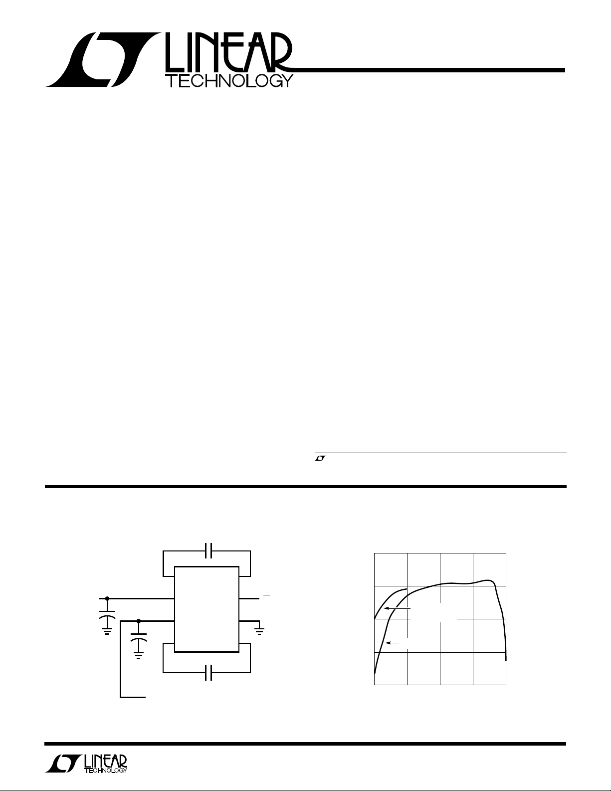
The LTC®1516 is a micropower charge pump DC/DC
converter that produces a regulated 5V output from a 2V
to 5V supply. Extremely low supply current (12µ A typical
with no load, <1µA in shutdown) and low external parts
count (two 0.22µ F flying capacitors and two 10µ F capacitors at VIN and V
) make the LTC1516 ideally suited for
OUT
small, light load battery-powered applications. Typical
efficiency (VIN = 3V) exceeds 70% with load currents
between 50µ A and 50mA. Modulating the SHDN pin keeps
the typical efficiency above 70% with load currents all the
way down to 10µA.
The LTC1516 operates as either a doubler or a tripler
depending on VIN and output load conditions to improve
overall efficiency. The part has thermal shutdown and can
survive a continuous short from V
to GND. In shut-
OUT
down the load is disconnected from VIN.
The LTC1516 is available in an 8-pin SO package in both
commercial and industrial temperature grades.
, LTC and LT are registered trademarks of Linear Technology Corporation.
TYPICAL APPLICATION
VIN = 2V TO 5V
Figure 1. Regulated 5V Output from a 2V to 5V Input
U
0.22µF
1
C1+
2
V
+
10µF
+
10µF
V
I
OUT
I
OUT
IN
LTC1516
3
V
OUT
4
+
C2
0.22µF
= 5V ±4%
OUT
= 0mA TO 20mA, VIN ≥ 2V
= 0mA TO 50mA, VIN ≥ 3V
C1–
SHDN
GND
C2
8
7
ON/OFF
6
5
–
1516 • F01
Efficiency vs Output Current
1
Page 2
LTC1516
WW
W
ABSOLUTE MAXIMUM RATINGS
U
U
W
PACKAGE/ORDER INFORMATION
(Note 1)
VIN to GND...................................................–0.3V to 6V
V
to GND ................................................–0.3V to 6V
OUT
SHDN to GND ..............................................–0.3V to 6V
V
Short-Circuit Duration............................. Indefinite
OUT
Operating Temperature Range
Commercial .............................................0°C to 70°C
Industrial ............................................ –40°C to 85°C
Storage Temperature Range................. –65°C to 150°C
Lead Temperature (Soldering, 10 sec)..................300°C
TOP VIEW
–
1
C1+
V
2
IN
V
3
OUT
+
C2
4
S8 PACKAGE
8-LEAD PLASTIC SO
T
= 125°C, θJA = 150°C/W
JMAX
Consult factory for Military grade parts.
C1
8
SHDN
7
GND
6
–
C2
5
ORDER PART
NUMBER
LTC1516CS8
LTC1516IS8
S8 PART MARKING
1516
1516I
ELECTRICAL CHARACTERISTICS
VIN = 2V to 5V, C1 = C2 = 0.22µF, CIN = C
SYMBOL PARAMETER CONDITIONS MIN TYP MAX UNITS
V
IN
V
OUT
I
CC
f
OSC
V
IH
V
IL
I
IH
I
IL
t
ON
The ● denotes specifications which apply over the full operating
temperature range.
Note 1: Absolute Maximum Ratings are those values beyond which the life
of the device may be impaired
Input Voltage ● 25V
Output Voltage 2V ≤ VIN ≤ 5V, I
Supply Current 2V ≤ VIN ≤ 5V, I
Output Ripple Full Load 100 mV
Efficiency VIN = 3V, I
Switching Frequency Full Load 600 kHz
SHDN Input Threshold ● (0.7)(VIN)V
SHDN Input Current V
V
Turn-On Time VIN = 3V, I
OUT
= 10µF, T
OUT
≤ V
≤ 3.6V, I
3V
IN
3.6V ≤ VIN ≤ 5V, I
2V ≤ VIN ≤ 5V, I
= V
SHDN
V
= 0V ● –1 1 µA
SHDN
to T
MIN
OUT
OUT
OUT
OUT
OUT
= 20mA 82 %
OUT
IN
= 0mA (Note 3) 500 µs
OUT
unless otherwise specified (Note 3).
MAX
≤ 20mA ● 4.8 5.2 V
≤ 50mA ● 4.8 5.2 V
≤ 50mA, TA = 25°C (Note 2) 4.8 5.2 V
= 0mA, SHDN = 0V ● 12 20 µA
= 0mA, SHDN = V
Note 2: At input voltages >3.6V and ambient temperatures >70°C,
continuous power dissipation must be derated to maintain junction
temperatures below 125°C. Derate 6mW/°C above 70°C in SO-8.
Note 3: The LTC1516 is tested with the capacitors shown in Figure 1.
IN
● 0.005 1 µA
● 0.4 V
● –1 1 µA
U
2
Page 3
W
U
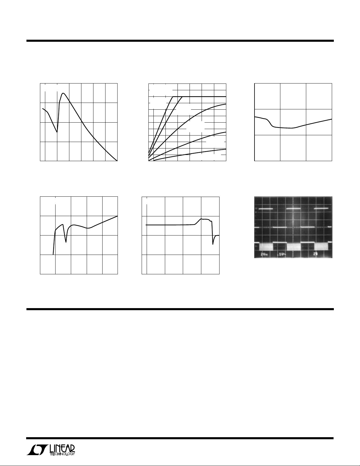
TYPICAL PERFORMANCE CHARACTERISTICS
Efficiency vs Input Voltage
90
= 10mA
I
OUT
80
Output Current vs Input Voltage
120
C
= 10µF
OUT
= 25°C
T
A
100
C1 = C2
80
= 0.22µF
C1 = C2
= 0.1µF
LTC1516
No Load Supply Current vs
Input Voltage
20
15
70
EFFICIENCY (%)
60
50
2.0 2.5 3.0 4.0 4.53.5
INPUT VOLTAGE (V)
Output Voltage vs Input Voltage
5.10
5.05
5.00
OUTPUT VOLTAGE (V)
4.95
4.90
= 20mA
I
OUT
2134
INPUT VOLTAGE (V)
1516 • G01
1516 • G04
5.0
5.10
5.05
5.00
OUTPUT VOLTAGE (V)
4.95
4.90
65
60
40
20
MAXIMUM OUTPUT CURRENT (mA)
0
234
C1 = C2
= 0.047µF
C1 = C2 = 0.01µF
INPUT VOLTAGE (V)
C1 = C2
= 0.022µF
Output Voltage vs Output Current
VIN = 3V
0.01 0.1 1 10 100
OUTPUT CURRENT (mA)
1516 • G05
1516 • G02
5
0mA TO 25mA,
10mA/DIV
AC COUPLED,
100mV/DIV
10
SUPPLY CURRENT (µA)
5
234
INPUT VOLTAGE (V)
Load Transient Response, VIN = 3V
I
,
OUT
V
,
OUT
1516 • G03
1516 • G04
5
UUU
PIN FUNCTIONS
C1+ (Pin 1): Flying Capacitor 1, Positive Terminal.
VIN (Pin 2): Input Supply Voltage.
V
(Pin 3): 5V Output Voltage (V
OUT
C2+ (Pin 4): Flying Capacitor 2, Positive Terminal.
C2– (Pin 5): Flying Capacitor 2, Negative Terminal.
= 0V in Shutdown).
OUT
GND (Pin 6): Ground.
SHDN (Pin 7): Active High CMOS Logic-Level Shutdown
Input.
C1– (Pin 8): Flying Capacitor 1, Negative Terminal.
3
Page 4

LTC1516
BLOCK DIAGRAM
V
IN
+
10µF
+
C2
0.22µF
–
C2
W
S1A
S1B
S2A
S2B
COMP1
SHDN
V
OUT
+
10µF
CLOCK 1
S1C
S2C
S1D
CHARGE PUMP
CLOCK 2
WUU
0.22µF
+
C1
–
C1
CHARGE PUMP SHOWN IN TRIPLER MODE, DISCHARGE CYCLE
U
APPLICATIONS IN FORMA TION
Operation
The LTC1516 uses a switched capacitor charge pump to
boost VIN from 2V to 5V to a regulated 5V ± 4% output
voltage. Regulation is achieved by sensing the output
voltage through an internal resistor divider and enabling
the charge pump when the output voltage droops below
the lower trip point of COMP2. When the charge pump is
enabled, a 2-phase, nonoverlapping clock controls the
charge pump switches. Clock 1 closes the S1 switches
which enable the flying capacitors, C1 and C2, to charge
up to the VIN voltage. Clock 2 closes the S2 switches which
stack C1 and C2 in series with VIN and connect the top
plate of C2 to the output capacitor at V
of charging and discharging continues at a free-running
frequency of 600kHz (typ) until the output has risen to the
upper trip point of COMP2 and the charge pump is
disabled. When the charge pump is disabled, the LTC1516
draws only 8µA (typ) from VIN which provides high
efficiency at low load conditions.
To achieve the highest efficiency over the entire VIN range,
the LTC1516 operates as either a doubler or a tripler
. This sequence
OUT
CONTROL
LOGIC
COMP2
COMP3
V
REF
V
OS
S3
LTC1516 • BD
depending on VIN and output load conditions. COMP1 and
COMP2 determine whether the charge pump is in doubler
mode or tripler mode. COMP1 forces the part into tripler
mode if VIN is <2.55V, regardless of output load. When V
IN
is >2.55V, the part will be in doubler mode using only C2
as a flying capacitor. In doubler mode, if the output droops
by 50mV under heavy loads, COMP3 will force the charge
pump into tripler mode until V
climbs above the upper
OUT
trip point of COMP3. Under these VIN and load conditions,
the nominal V
the no load nominal V
output load results in efficiency greater than 80% with V
will be approximately 50mV lower than
OUT
. This method of sensing VIN and
OUT
IN
between 2.5V and 3V.
In shutdown mode, all circuitry is turned off and the part
draws only leakage current (<1µA) from the VIN supply.
V
is also disconnected from VIN. The SHDN pin is a
OUT
CMOS input with a threshold of approximately VIN/2;
however, the SHDN pin can be driven by logic levels that
exceed the VIN voltage. The part enters shutdown mode
when a logic high is applied to the SHDN pin. The SHDN pin
cannot float; it must be driven with a logic high or low.
4
Page 5

LTC1516
U
WUU
APPLICATIONS IN FORMA TION
Short-Circuit/Thermal Protection
During short-circuit conditions, the LTC1516 will draw
between 200mA and 400mA from VIN causing a rise in
the junction temperature. On-chip thermal shutdown
circuitry disables the charge pump once the junction
temperature exceeds 135°C, and reenables the charge
pump once the junction temperature falls back to 115°C.
The LTC1516 will cycle in and out of thermal shutdown
indefinitely without latchup or damage until the V
is removed.
Capacitor Selection
For best performance, it is recommended that low ESR
capacitors be used for both CIN and C
and ripple. The CIN and C
capacitors should be either
OUT
to reduce noise
OUT
ceramic or tantalum and should be 10µ F or greater. If the
input source impedance is very low, CIN may not be
needed. Increasing the size of C
to 22µ F or greater will
OUT
reduce output voltage ripple.
Ceramic or tantalum capacitors are recommended for the
flying caps C1 and C2 with values in the range of 0.1µ F to
1µ F. Note that large value flying caps (>0.22µF) will
increase output ripple unless C
is also increased. For
OUT
very low load applications, C1 and C2 may be reduced to
0.01µF to 0.047µF. This will reduce output ripple at the
expense of efficiency and maximum output current.
Output Ripple
OUT
short
higher ripple due to higher output voltage dV/dt. High ESR
capacitors (ESR > 0.5Ω) on the output pin cause high
frequency voltage spikes on V
with every clock cycle.
OUT
There are several ways to reduce the output voltage ripple.
A larger C
the low and high frequency ripple due to the lower C
capacitor (22µ F or greater) will reduce both
OUT
OUT
charging and discharging dV/dt and the lower ESR typically found with higher value (larger case size) capacitors.
A low ESR ceramic output capacitor will minimize the high
frequency ripple, but will not reduce the low frequency
ripple unless a high capacitance value is chosen. A reasonable compromise is to use a 10µF to 22µF tantalum
capacitor in parallel with a 1µ F to 3.3µ F ceramic capacitor
on V
to reduce both the low and high frequency ripple.
OUT
An RC filter may also be used to reduce high frequency
voltage spikes (see Figure 2).
In low load or high VIN applications, smaller values for C1
and C2 may be used to reduce output ripple. The smaller
C1 and C2 flying capacitors (0.022µ F to 0.1µF) deliver less
charge per clock cycle to the output capacitor resulting in
lower output ripple. However, the smaller value flying caps
also reduce the maximum I
capability as well as
OUT
efficiency.
LTC1516
3
V
OUT
+
15µF
TANTALUM
1µF
CERAMIC
V
OUT
5V
Normal LTC1516 operation produces voltage ripple on the
V
pin. Output voltage ripple is required for the LTC1516
OUT
to regulate. Low frequency ripple exists due to the hysteresis in the sense comparator and propagation delays in the
charge pump enable/disable circuits. High frequency ripple
is also present mainly due to ESR (Equivalent Series
Resistance) in the output capacitor. Typical output ripple
under maximum load is 100mV
with a low ESR 10µF
P-P
output capacitor.
The magnitude of the ripple voltage depends on several
factors. High input voltages (VIN > 3.3V) increase the output
ripple since more charge is delivered to C
per clock
OUT
cycle. Large C1 and C2 flying capacitors (> 0.22µF) also
increase ripple for the same reason. Large output current
load and/or a small output capacitor (< 10µF) results in
LTC1516
Figure 2. Output Ripple Reduction Techniques
3
V
OUT
+
10µF
2Ω
V
OUT
+
5V
10µF
1516 F02
Inrush Currents
During normal operation, VIN will experience current transients in the 100mA to 200mA range whenever the charge
pump is enabled. During start-up, these inrush currents
may approach 500mA. For this reason, it is important to
minimize the source resistance between the input supply
and the VIN pin to prevent start-up problems and large
input voltage transients.
5
Page 6

LTC1516
OUTPUT CURRENT (µA)
1
10
100
1000
MAXIMUM SHDN OFF TIME (ms)
1000
1516 • F04b
1 10 100
SHDN ON PULSE WIDTH = 200µs
C
OUT
= 10µF
U
WUU
APPLICATIONS IN FORMA TION
Ultralow Quiescent Current (IQ < 5µA) Regulated
Supply
The LTC1516 contains an internal resistor divider (refer to
Block Diagram) which draws only 1.5µ A (typ) from V
During no-load conditions, the internal load causes a
droop rate of only 150mV per second on V
C
= 10µ F. Applying a 5Hz to 100Hz, 95% to 98% duty
OUT
OUT
cycle signal to the SHDN pin ensures that the circuit of
Figure 3 comes out of shutdown frequently enough to
maintain regulation during no-load or low-load conditions. Since the part spends nearly all of its time in
shutdown, the no-load quiescent current (see Figure 4a) is
approximately equal to (V
)(1.5µA)/(VIN)(Efficiency).
OUT
0.22µF
1
C1+
C1–
8
OUT
with
.
The LTC1516 must be out of shutdown for a minimum
duration of 200µ s to allow enough time to sense the output
and keep it in regulation. As the V
load current
OUT
increases, the frequency with which the part is taken out
of shutdown must also be increased to prevent V
OUT
from drooping below 4.8V during the OFF phase (see
Figure 4b). A 100Hz 98% duty cycle signal on the SHDN
pin ensures proper regulation with load currents as high
as 100µA. When load current greater than 100µA is
needed, the SHDN pin must be forced low as in normal
operation. The typical no-load supply current for this
circuit with VIN = 3V is only 3.2µA.
VIN = 2V TO 5V
Figure 4a. No Load ICC vs Input Voltage for Circuit in Figure 3
+
10µF
+
10µF
V
= 5V ±4%
OUT
6.0
4.0
2.0
SUPPLY CURRENT (µA)
0.0
2.0 3.0 4.0
INPUT VOLTAGE (V)
2
V
IN
LTC1516
3
V
OUT
4
+
C2
0.22µF
SHDN
GND
C2
7
FROM MPU
6
5
–
SHDN PIN WAVEFORMS:
LOW I
MODE (5Hz TO 100Hz, 95% TO 98% DUTY CYCLE)
Q
≤ 100µA
I
OUT
Figure 3. Ultralow Quiescent Current (<5µA) Regulated Supply
5.0
1516 • F04a
Figure 4b. Maximum SHDN OFF Time vs Output Load Current for
Ultralow IQ Operation
V
LOAD ENABLE MODE
OUT
= 100µA TO 50mA)
(I
OUT
1516 • F03
6
Page 7

LTC1516
C2
C
OUT
C
IN
V
OUT
V
IN
1516 • F06
LTC1516
18
27
36
45
SHDN
GND
+
+
C1
U
WUU
APPLICATIONS IN FORMA TION
Paralleling Devices
Two or more LTC1516’s may be connected in parallel to
provide higher output currents. The VIN, V
SHDN pins may be tied together, but the C1 and C2 pins
must be kept separate (see Figure 5). Separate CIN and
C
capacitors may be required to reduce output noise
OUT
and ripple if the paralleled devices cannot be kept close
together. Otherwise, single CIN and C
OUT
be used with each being 2× (or 3× if three parts are
paralleled, etc.) in value.
0.22µF
1
C1+
2
V
IN
LTC1516
3
V
OUT
4
+
C2
C1–
SHDN
GND
C2
, GND and
OUT
capacitors may
8
7
6
5
–
General Layout Considerations
Due to the high switching frequency and high transient
currents produced by the LTC1516, careful board layout is
a must. A clean board layout using a ground plane and
short connections to all capacitors will improve performance and ensure proper regulation under all conditions
(refer to Figure 6).
0.22µF
0.22µF
1
C1+
VIN = 2V
TO 5V
+
22µF
+
Figure 5. Paralleling Devices
2
V
IN
LTC1516
3
V
OUT
22µF
4
+
C2
0.22µF
V
= 5V ±4%
OUT
= 0mA TO 40mA, VIN ≥ 2V
I
OUT
= 0mA TO 100mA, VIN ≥ 3V
I
OUT
C1–
SHDN
GND
C2
Figure 6. Suggested Component Placement for LTC1516
8
7
6
5
–
ON/OFF
1516 • F05
Information furnished by Linear Technology Corporation is believed to be accurate and reliable.
However, no responsibility is assumed for its use. Linear Technology Corporation makes no representation that the interconnection of its circuits as described herein will not infringe on existing patent rights.
7
Page 8

LTC1516
0.1µF
ON/OFF
10µF
10µF
0.1µF 0.22µF
V
IN
2V TO 5V
CENTRAL SEMICONDUCTOR CMPSH-35 DUAL SCHOTTKY
OPTIONAL CIRCUITRY FOR MAINTAINING –V
OUT
AT LOW V
OUT
LOADS
Q1, Q2: 2N3904
*
**
+
2.2µF
8.2k
3.3k
*
**
1516 • TA03
240Ω
V
OUT
= 5V ±4%
I
OUT
= 20mA,VIN ≥ 2V
I
OUT
= 50mA, VIN ≥ 3V
–V
OUT
= –1.4V TO –3V
–I
OUT
= 5mA
1
7
2
4
8
3
6
5
C1
+
LTC1516
V
IN
SHDN
C2
+
C1
–
V
OUT
GND
C2
–
Q2Q1
+
U
TYPICAL APPLICATIONS N
Fault-Protected SIM Interface Supply for
GSM Cellular Phones
0.1µF
Generating 5V and a Negative Supply
3V
GSM
CONTROLLER
+
10µF
1
C1
2
V
7
SHDN
4
C2
+
V
IN
LTC1516
+
0.1µF
LEVEL SHIFT
C1
OUT
GND
C2
8
–
3
+
6
5
–
10µF
PACKAGE DESCRIPTION
0.010 – 0.020
(0.254 – 0.508)
0.008 – 0.010
(0.203 – 0.254)
*
DIMENSION DOES NOT INCLUDE MOLD FLASH. MOLD FLASH
SHALL NOT EXCEED 0.006" (0.152mm) PER SIDE
**
DIMENSION DOES NOT INCLUDE INTERLEAD FLASH. INTERLEAD
FLASH SHALL NOT EXCEED 0.010" (0.254mm) PER SIDE
× 45°
0°– 8° TYP
0.016 – 0.050
0.406 – 1.270
V
= 5V ±4%
OUT
= 40mA
I
OUT
V
CC
RST
CLK
SIM CARD
I/O
GND
1516 • TA02
U
Dimensions in inches (millimeters) unless otherwise noted.
S8 Package
8-Lead Plastic Small Outline (Narrow 0.150)
(LTC DWG # 05-08-1610)
0.189 – 0.197*
(4.801 – 5.004)
0.053 – 0.069
(1.346 – 1.752)
0.014 – 0.019
(0.355 – 0.483)
0.004 – 0.010
(0.101 – 0.254)
0.050
(1.270)
BSC
0.228 – 0.244
(5.791 – 6.197)
8
1
7
2
5
6
0.150 – 0.157**
(3.810 – 3.988)
SO8 0695
3
4
RELATED PARTS
PART NUMBER DESCRIPTION COMMENTS
LT®1054 100mA Switched Capacitor Converter Includes Reference and Amplifier for Regulation
LTC1144 20mA Switched Capacitor Converter for Up to 20V Inputs Includes Micropower Shutdown (8µA)
LTC1261 Positive to Negative Regulated Switched Capacitor Converter Low Noise (5mV) Output for Up to 10mA Loads
LTC1262 5V to 12V Regulated Switched Capacitor Converter Up to 30mA at Regulated Output
LTC1550/51 Low Noise Switched Capacitor Regulated Converter Provides –4.1V at 20mA with <1mV Ripple
Linear Technology Corporation
8
1630 McCarthy Blvd., Milpitas, CA 95035-7417
(408) 432-1 900
●
FAX
: (408) 434-0507
●
TELEX
: 499-3977
LT/GP 0796 7K • PRINTED IN USA
LINE AR TECHNOLO GY CORP O RATION 1 996
 Loading...