

Page 1
FEATURES
LTC1515 Series
Step-Up/Step-Down
Switched Capacitor DC/DC
Converters with Reset
U
DESCRIPTION
■
Adjustable/Selectable 3V, 3.3V or 5V
Output Voltages
■
2V to 10V Input Voltage Range
■
Up to 50mA Output Current
■
Only Three External Capacitors Required
■
Soft Start Limits Inrush Current at Turn-On
■
Low Operating Current: 60µA
■
Very Low Shutdown Current: < 1µA
■
Shutdown Disconnects Load from V
■
V
Programmable to 3V/5V or 3.3V/5V
OUT
■
Short-Circuit and Overtemperature Protected
■
650kHz Switching Frequency
■
Open-Drain Power-On Reset Output
■
Available in SO-8 Package
Daisy-Chained Control Outputs
IN
U
APPLICATIONS
■
SIM Interface in GSM Cellular Telephones
■
Smart Card Readers
■
Local Power Supplies
■
Portable Equipment
The LTC®1515, LTC1515-3/5 and LTC1515-3.3/5 are
micropower switched capacitor DC/DC converters that
produce a regulated output voltage by either stepping up
or stepping down the input voltage. Output voltage is
adjustable using an external resistor divider (LTC1515) or
programmable to either 3V/5V (LTC1515-3/5) or 3.3V/5V
(LTC1515-3.3/5) using a logic pin.
A unique architecture allows the parts to accommodate a
wide input voltage range (2V to 10V) while maintaining
± 4% regulation. Additional circuitry prevents excessive
inrush current and output voltage ripple when large VIN to
V
differentials are present.
OUT
An internal power-on reset circuit forces the POR pin low
on initial power-up. The POR output remains low until
200ms (typ) after V
is in regulation.
OUT
The parts are short-circuit and overtemperature protected.
Battery life is maximized by very low operating currents
(ICC = 60µ A typ, ICC < 1µ A in shutdown). All three parts are
available in an SO-8 package.
, LTC and LT are registered trademarks of Linear Technology Corporation.
U
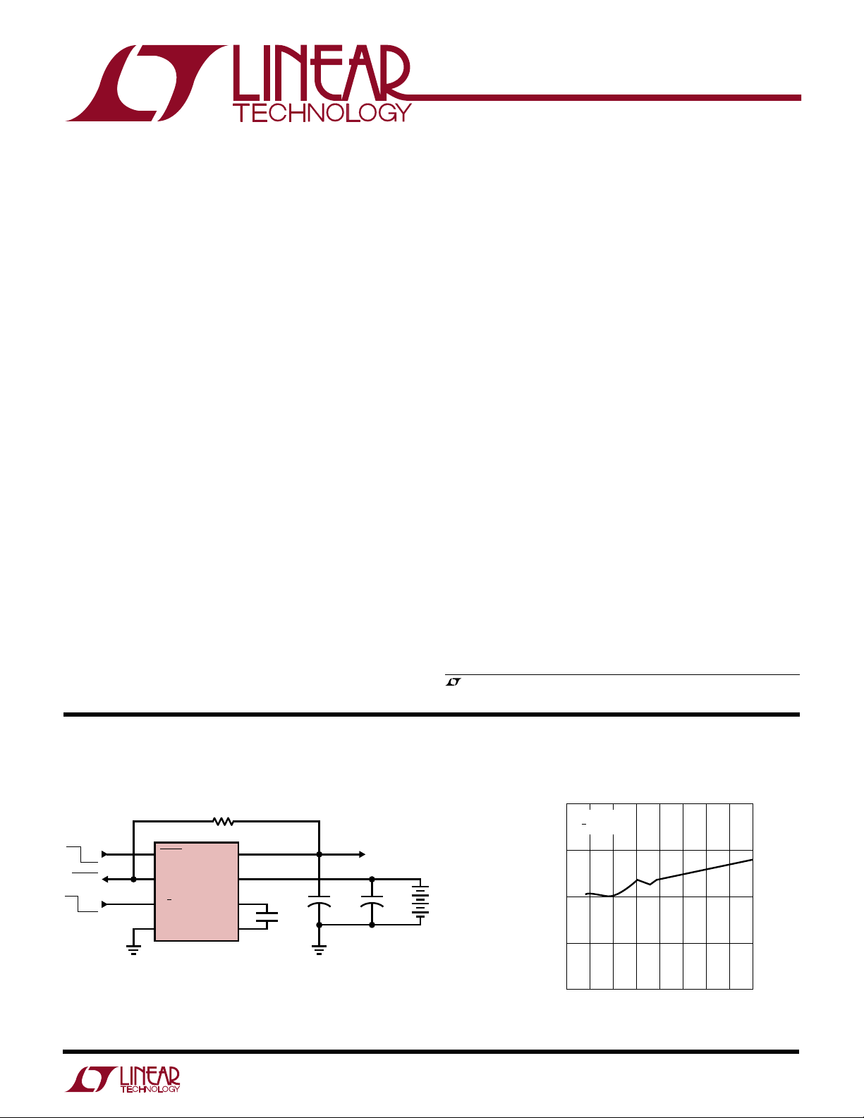
TYPICAL APPLICATION
Programmable 3.3V/5V Power Supply with Power-On Reset
100k
ON OFF
RESET
5V 3.3V
1
SHDN
2
POR
LTC1515-3.3/5
3
5/3
4
GND
8
V
OUT
7
V
IN
6
+
C1
–
C1
0.22µF
5
10µF 10µF
V
OUT
I
OUT
++
= 3.3V OR 5V
= 50mA
LTC1515 • TA01
V
IN
4-CELL
NiCd
LTC1515-X 5V Output vs Input Voltage
5.2
I
= 10mA
OUT
5/3 = 3V
5.1
5.0
OUTPUT VOLTAGE (V)
4.9
4.8
2
4
3
INPUT VOLTAGE (V)
5
6
8
7
9
LT1515 • TA02
10
1
Page 2
LTC1515 Series
WW
W
U
ABSOLUTE MAXIMUM RATINGS
(Note 1)
VIN to GND................................................ –0.3V to 12V
V
to GND ............................................. – 0.3V to 12V
OUT
SHDN, 5/3, FB to GND.............................. – 0.3V to 12V
V
Short-Circuit Duration............................. Indefinite
OUT
/
PACKAGE
SHDN
POR
FB
GND
T
JMAX
Consult factory for Military grade parts.
O
RDER I FOR ATIO
TOP VIEW
1
2
3
4
S8 PACKAGE
8-LEAD PLASTIC SO
= 125°C, θJA = 110°C/W
V
8
OUT
VIN
7
+
C1
6
–
C1
5
WU
ORDER PART
NUMBER
LTC1515CS8
LTC1515IS8
S8 PART MARKING
1515
1515I
U
Operating Temperature Range
Commercial .............................................0°C to 70°C
Industrial ............................................ –40°C to 85°C
Storage Temperature Range ................ –65°C to 150°C
Lead Temperature (Soldering, 10 sec)................. 300°C
ORDER PART NUMBER
LTC1515CS8-3/5
LTC1515CS8-3.3/5
LTC1515IS8-3/5
LTC1515IS8-3.3/5
S8 PART MARKING
151535
515335
515I35
15I335
1
SHDN
POR
2
5/3
3
GND
4
8-LEAD PLASTIC SO
T
= 125°C, θJA = 110°C/W
JMAX
TOP VIEW
S8 PACKAGE
V
8
OUT
VIN
7
+
C1
6
–
C1
5
ELECTRICAL CHARACTERISTICS
VIN = 2V to 10V, SHDN = 3V, C1 = 0.22µF, CIN = C
PARAMETER CONDITIONS MIN TYP MAX UNITS
Operating Voltage V
V
IN
= 3V (LTC1515-3/5) 2V ≤ VIN ≤ 8V, I
V
OUT
= 3.3V (LTC1515-3.3/5) 2V ≤ VIN ≤ 8V, I
V
OUT
= 5V (LTC1515-3/5, LTC1515-3.3/5) 2.7V ≤ VIN ≤ 10V, I
V
OUT
VFB Feedback Voltage LTC1515, VFB Ramping Negative ● 1.190 1.232 1.275 V
VFB Feedback Hysteresis LTC1515 1 %
Effective Output Resistance LTC1515, VIN = 3V, Step-Up Mode ● 30 Ω
Operating Current VIN ≤ 5V, I
V
IN
Shutdown Current SHDN = 0V, VIN ≤ 5V ● 1 µA
V
IN
Output Ripple Full Load (Note 2) 100 mV
Switching Frequency Full Load ● 500 650 800 kHz
5/3, SHDN Input Threshold V
5/3, SHDN Input Current 5/3, SHDN = V
FB Input Current FB = 1.232V ● –50 50 nA
POR Output Low Voltage I
= 10µF unless otherwise noted (Note 2).
OUT
= 5V ● 2.7 10 V
OUT
= 3V/3.3V ● 2.0 8 V
V
OUT
V
= ADJ ● 2.0 10 V
OUT
≤ 15mA ● 2.88 3.0 3.12 V
3V ≤ VIN ≤ 8V, I
3V ≤ VIN ≤ 8V, I
3.3V ≤ VIN ≤ 10V, I
VIN > 5V, I
SHDN = 0V, VIN > 5V 25 µA
IL
V
IH
5/3, SHDN = 0V ● –1 1 µA
= 100µA, VIN = 3V ● 0.05 0.4 V
SINK
OUT
≤ 50mA ● 2.88 3.0 3.12 V
OUT
≤ 15mA ● 3.17 3.3 3.43 V
OUT
≤ 50mA ● 3.17 3.3 3.43 V
OUT
≤ 15mA ● 4.8 5.0 5.2 V
OUT
≤ 50mA ● 4.8 5.0 5.2 V
OUT
= 0, SHDN = 3V ● 60 100 µA
OUT
= 0, SHDN = 3V ● 75 135 µA
OUT
● 0.4 1.0 V
● 1.0 1.6 V
IN
● –1 1 µA
P-P
2
Page 3
LTC1515 Series
INPUT VOLTAGE (V)
0
OPERATING CURRENT (µA)
120
100
80
60
40
20
8
1515 G06
2
4
6
10
85°C
–40°C
25°C
V
OUT
= 5V
I
OUT
= 0mA
INPUT VOLTAGE (V)
0
OUTPUT VOLTAGE RIPPLE (mV
P-P
)
250
200
150
100
50
0
8
1515 G03
2
4
6
10
V
OUT
= 3.3V
I
OUT
= 10mA
T
A
= 25°C
C
OUT
= 10µF
C
OUT
= 22µF
C
OUT
= 47µF
ELECTRICAL CHARACTERISTICS
VIN = 2V to 10V, SHDN = 3V, C1 = 0.22µF, CIN = C
PARAMETER CONDITIONS MIN TYP MAX UNITS
POR Leakage Current V
POR Trip Point (With Respect to V
POR Trip Point Hysteresis 1%
I
Short-Circuit Current V
OUT
t
ON
POR Delay After V
The
● denotes specifications which apply over the full operating
temperature range.
Note 1: Absolute Maximum Ratings are those values beyond which the life
of the device may be impaired.
)V
OUT
= 10µF unless otherwise noted (Note 2).
OUT
= 5V ● –1 1 µA
POR
Ramping Negative ● –10 –7.5 –5 %
OUT
= 0V ● 12 40 mA
OUT
Soft Start Turn-On Time 4 ms
Above POR Threshold ● 140 200 280 ms
OUT
Note 2: For V
≥ 8V, C
IN
OUT
= 22µF.
UW
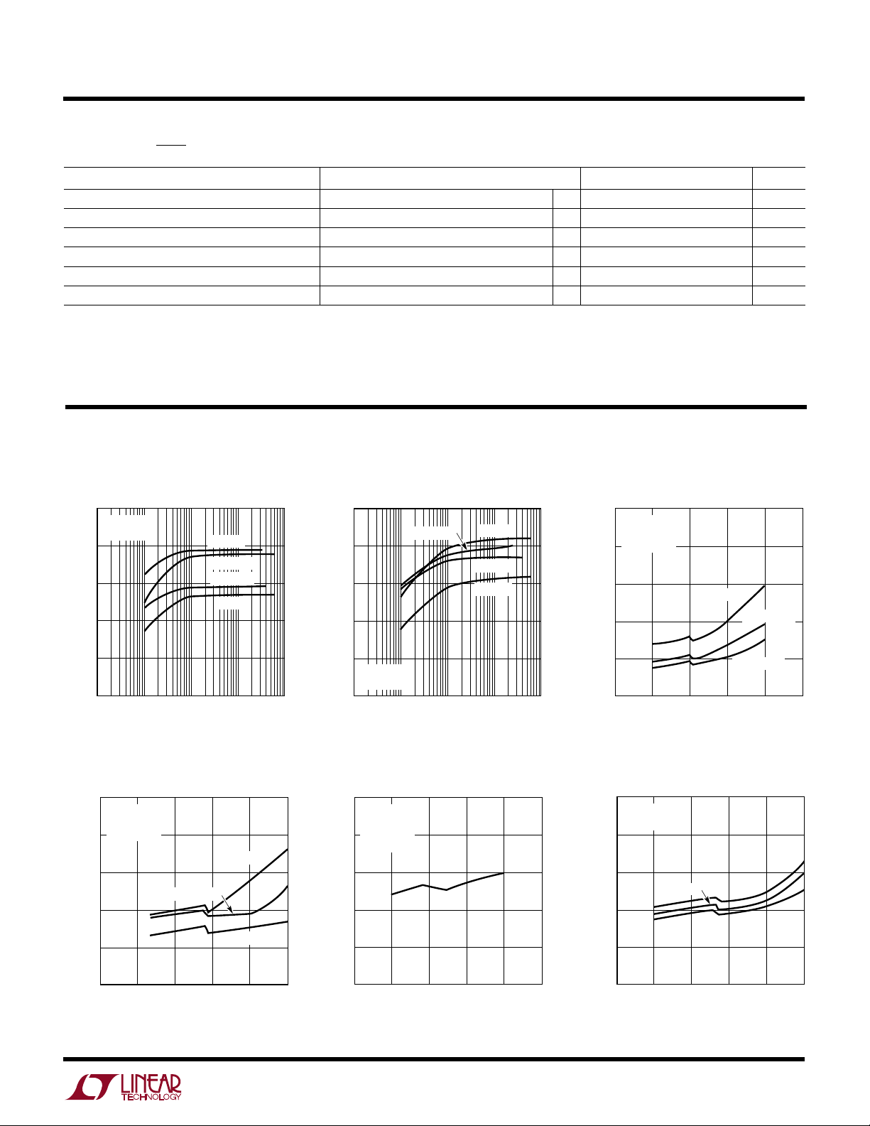
TYPICAL PERFORMANCE CHARACTERISTICS
LTC1515-X
3.3V Efficiency vs Output Current
100
V
= 3.3V
OUT
= 25°C
T
A
80
60
40
EFFICIENCY (%)
20
0
0.01 1 10
LTC1515-X 5V Output Voltage
Ripple vs Input Voltage
250
V
OUT
)
I
OUT
P-P
OUTPUT VOLTAGE RIPPLE (mV
200
150
100
= 25°C
T
A
50
0
0
VIN = 2V
VIN = 4.4V
VIN = 2.7V
VIN = 6V
0.1 100
OUTPUT CURRENT (mA)
= 5V
= 10mA
C
= 10µF
OUT
C
= 22µF
OUT
C
= 47µF
OUT
2
INPUT VOLTAGE (V)
4
6
8
1515 G01
1515 G04
LTC1515-X
5V Efficiency vs Output Current
100
80
60
40
EFFICIENCY (%)
20
V
OUT
= 25°C
T
A
0
0.01 1 10
VIN = 2.7V
= 5V
0.1 100
OUTPUT CURRENT (mA)
VIN = 6V
VIN = 3.3V
VIN = 8V
1515 G02
LTC1515-X 3.3V Output Voltage
vs Input Voltage
3.45
V
= 3.3V
OUT
= 10mA
I
OUT
= 10µF
C
3.40
OUT
= 25°C
T
A
3.35
3.30
OUTPUT VOLTAGE (V)
3.25
10
3.20
2
0
INPUT VOLTAGE (V)
6
8
4
10
1515 G05
LTC1515-X 3.3V Output Voltage
Ripple vs Input Voltage
LTC1515-X Operating Current
vs Input Voltage
3
Page 4

LTC1515 Series
INPUT VOLTAGE (V)
2
EFFICIENCY (%)
100
80
60
40
20
10
1515 G08
4
6
8
12
V
OUT
= 5V
I
OUT
= 10mA
TA = 25°C
UW
TYPICAL PERFORMANCE CHARACTERISTICS
LTC1515-X
3V Efficiency vs Input Voltage
100
80
60
EFFICIENCY (%)
40
20
2
0
4
INPUT VOLTAGE (V)
LTC1515-X Shutdown Supply
Current vs Input Voltage
25
SHDN = 0V
20
15
10
5
POSITIVE SUPPLY CURRENT (µA)
0
2
0
4
INPUT VOLTAGE (V)
6
–40°C
6
V
I
T
OUT
OUT
A
= 3V
= 10mA
= 25°C
8
25°C
8
1515 G09
85°C
1515 G12
10
AC COUPLED
10
100
80
60
EFFICIENCY (%)
40
20
V
OUT
100mV/DIV
I
OUT
50mA/DIV
LTC1515-X
3.3V Efficiency vs Input Voltage
V
= 3.3V
OUT
= 10mA
I
OUT
TA = 25°C
2
0
INPUT VOLTAGE (V)
6
4
8
1515 G07
LTC1515-X Step-Down Mode
5V Load Transient Response
VIN = 8V, V
OUT
= 5V, C
= 10µF, TA = 25°C
OUT
1515 G10
10
50mA
0mA
V
OUT
AC COUPLED
100mV/DIV
I
OUT
50mA/DIV
LTC1515-X
5V Efficiency vs Input Voltage
LTC1515-X Step-Up Mode
5V Load Transient Response
VIN = 3.3V, V
OUT
= 5V, C
= 10µF, TA = 25°C
OUT
1515 G11
PIN FUNCTIONS
SHDN (Pin 1): Shutdown Input. A logic low on the SHDN
pin puts the part into shutdown mode. A logic high (V
≥ 1.6V) enables the part. At high VIN voltages, the SHDN
pin may still be controlled with 3V logic without causing a
large rise in VIN quiescent current. The SHDN pin may not
float; connect to VIN if unused.
POR (Pin 2): Open-Drain Power-On Reset Output. This pin
will pull low upon initial power-up, during shutdown or
until V
more than 200ms typ.
5/3 (LTC1515-X) (Pin 3): Output Voltage Select. A logic
high on the 5/3 pin will force V
4
OUT
UUU
SHDN
has been within 6.5% of its regulated value for
to regulate to 5V. A logic
OUT
low will force V
to 3V (LTC1515-3/5) or 3.3V (LTC1515-
OUT
3.3/5). As with the SHDN pin, the 5/3 pin may be driven with
3V logic over the entire VIN range. The 5/3 pin may not float.
FB (LTC1515) (Pin 3): Feedback Input. The voltage on this
pin is compared to the internal reference voltage (1.232V)
to keep the output in regulation. An external resistor divider
is required between V
and FB to adjust the output
OUT
voltage. Total divider resistance should not exceed 2M.
GND (Pin 4): Ground. Should be tied to a ground plane for
best performance.
C1– (Pin 5): Charge Pump Flying Capacitor, Negative
Terminal.
Page 5

UUU
PIN FUNCTIONS
LTC1515 Series
C1+ (Pin 6): Charge Pump Flying Capacitor, Positive
Terminal.
VIN (Pin 7): Charge Pump Input Voltage. May be between
2V and 10V. VIN should be bypassed with a ≥ 10µF low
ESR capacitor as close as possible to the pin for best
performance.
WW
SI PLIFIED
BLOCK DIGRAM
V
IN
SHDN
650kHz
OSCILLATOR
POR
RESET
COUNTER
C1
STEP-UP/STEP-DOWN
EN
EN
V
(Pin 8): Regulated Output Voltage. Pin selectable to
OUT
either 3V/5V, 3.3V/5V or adjustable using an external
resistor divider (LTC1515). V
should be bypassed with
OUT
a ≥ 10µF low ESR capacitor as close as possible to the pin
for best performance.
–
CHARGE PUMP
+
C1
V
(LTC1515-X)
(LTC1515-X)
–
+
–
V
OS
+
1.232V
V
REF
OUT
FB
(LTC1515)
5/3
(LTC1515-X)
U
WUU
APPLICATIONS INFORMATION
Regulator Operation
The regulator section of the LTC1515, LTC1515-3/5 and
LTC1515-3.3/5 consists of a charge pump, reference,
comparator and some logic. The divided down output
voltage is compared to the internal reference voltage.
When the divided output drops below the reference voltage, the charge pump is enabled, which boosts the output
back into regulation. Hysteresis in the comparator forces
the regulator to burst on and off and causes approximately
100mV of peak-to-peak ripple to appear at the output. By
enabling the charge pump only when needed, the parts
achieve high efficiencies with low output load currents.
LTC1515 • BD
GND
Each part’s charge pump has a unique architecture that
allows the input voltage to be either stepped up or stepped
down to produce a regulated output. Internal circuitry
senses the VIN to V
differential voltage and controls the
OUT
charge pump operating mode. In addition, the effective
output impedance of the charge pump is internally
adjusted to prevent large inrush currents and allow for a
wide input voltage range. When the input voltage is lower
than the output voltage, the charge pump operates as a
step-up voltage doubler. When the input voltage is greater
than the output, the charge pump operates as a step-down
gated switch.
5
Page 6

LTC1515 Series
+
–
+
–
I
OUT
C
OUT
2V
IN
R
OUT
V
OUT
LT1515 • F02
U
WUU
APPLICATIONS INFORMATION
Output Voltage Selection
The LTC1515-X versions have internal resistor networks
which set the output voltage. The 5/3 pin controls an
internal switch that shorts out a portion of the resistor
network to change the output voltage. A logic high on this
pin produces a 5V output and a low produces either a 3V
output or a 3.3V output.
The output voltage of the LTC1515 is selected using an
external resistor divider (see Figure 1). The output voltage
is determined using the following formula:
V
= (1.232V)[1 + (R1/R2)]
OUT
The total resistance of R1 and R2 should not exceed 2M,
otherwise excess ripple may appear at V
Figure 1. LTC1515 Output Voltage Selection
Maximum V
OUT
R1
R2
and I
1
SHDN
2
POR
3
FB
4
GND
Calculations for the LTC1515
OUT
LTC1515
V
OUT
V
IN
C1
C1
LTC1515 • F01
+
–
The maximum output voltage and current available with
the LTC1515 can be calculated based on the effective
output resistance of the charge pump and the open circuit
output voltage. In step-up mode, the open circuit output
voltage is approximately 2VIN (see Figure 2). In step-down
mode, the open circuit output voltage equals VIN. The
relationship between R
and VIN in step-up mode is shown
OUT
in Figure 3.
The following formulas can be used to find the maximum
output voltage that may be programmed using the LTC1515
for a given minimum input voltage and output current
load.
.
OUT
8
7
6
5
Figure 2. Step-Up Mode Equivalent Circuit
40
OUTPUT RESISTANCE (Ω)
Figure 3. Step-Up Mode R
down mode, R
30
20
10
0
OUT
1
I
= 20mA
OUT
I
= 50mA
OUT
2
3
INPUT VOLTAGE (V)
4
LT1515 • F03
vs Input Voltage
OUT
5
is internally adjusted to ensure that the
maximum output current rating can be met.
Capacitor Selection
For best performance, low ESR capacitors are recommended for both CIN and C
The CIN and C
capacitors should be either ceramic or
OUT
to reduce noise and ripple.
OUT
tantalum and should be 10µ F or greater. If the input source
impedance is very low (< 0.5Ω) CIN may not be needed.
Increasing the size of C
to 22µ F or greater will reduce
OUT
output voltage ripple —particularly with high VIN voltages
(8V or greater). A ceramic capacitor is recommended for
the flying capacitor C1 with a value of 0.1µF or 0.22µF.
Smaller values may be used in low output current
applications.
Output Ripple
Step-Up Mode: Max V
Step-Down Mode: Max V
When VIN – (I
V
, the part will automatically switch from step-down
OUT
mode to step-up mode. In both step-up mode and step-
6
OUT
)(R
= (2)(Min VIN) – (I
OUT
= (Min VIN) – (I
OUT
) is less than the programmed
OUT
OUT
OUT
)(R
)(R
OUT
OUT
Normal LTC1515 series operation produces voltage ripple
)
on the V
)
parts to regulate. Low frequency ripple exists due to the
pin. Output voltage ripple is required for the
OUT
hysteresis in the sense comparator and propagation delays in the charge pump enable/disable circuits. High
frequency ripple is also present mainly from the ESR
Page 7

LTC1515 Series
U
WUU
APPLICATIONS INFORMATION
(equivalent series resistance) in the output capacitor.
Typical output ripple (V
100mV peak-to-peak with a low ESR, 10µ F output capacitor. For applications requiring VIN to exceed 8V, a 22µ F or
larger C
capacitor is recommended to maintain maxi-
OUT
mum ripple in the 100mV range.
The magnitude of the ripple voltage depends on several
factors. High input voltages increase the output ripple
since more charge is delivered to C
A large C1 flying capacitor (> 0.22µ F) also increases ripple
in step-up mode for the same reason. Large output
current load and/or a small output capacitor (<10µF)
results in higher ripple due to higher output voltage dV/dt.
High ESR capacitors (ESR > 0.5Ω) on the output pin cause
high frequency voltage spikes on V
cycle.
There are several ways to reduce the output voltage ripple.
A large C
capacitor (22µF or greater) will reduce both
OUT
the low and high frequency ripple due to the lower C
charging and discharging dV/dt and the lower ESR typically found with higher value (larger case size) capacitors.
A low ESR (<0.5Ω) ceramic output capacitor will minimize the high frequency ripple, but will not reduce the low
frequency ripple unless a high capacitance value is chosen. A reasonable compromise is to use a 10µF to 22µF
tantalum capacitor in parallel with a 1µ F to 3.3µF ceramic
capacitor on V
to reduce both the low and high
OUT
frequency ripple. An RC or LC filter may also be used to
reduce high frequency voltage spikes (see Figure 4).
LTC1515/
LTC1515-X
8
V
OUT
LTC1515/
LTC1515-X
8
V
OUT
Figure 4. Output Ripple Reduction Techniques
Inrush Currents
A common problem with switched capacitor regulators is
inrush current—particularly during power-up and com-
< 8V) under maximum load is
IN
per charging cycle.
OUT
with every clock
OUT
V
+
15µF
TANTALUM
2Ω
+ +
10µF
TANTALUM
OUT
1µF
CERAMIC
V
OUT
10µF
TANTALUM
LT1515 • F04
OUT
ing out of shutdown mode. Whenever large V
VIN) to V
voltage differentials are present, most charge
OUT
(or boosted
IN
pumps will pull large current spikes from the input supply.
Only the effective charge pump output impedance limits
the current while the charge pump is enabled. This may
disrupt input supply regulation, especially if the input
supply is a low power DC/DC converter or linear regulator.
The LTC1515 family minimizes inrush currents both at
start-up and under high VIN to V
Internal soft start circuitry controls the rate at which V
operation.
OUT
OUT
may be charged from 0V to its final regulated value. The
typical start-up time from V
corresponds to an effective V
= 0V to 5V is 4ms. This
OUT
charging current of only
OUT
12.5mA for a 10µF output capacitor (27.5mA for 22µF,
etc.). Note that any output current load present during
start-up will add directly to the charging currents mentioned above. The soft start circuitry limits start-up current both at initial power-up and when coming out of
shutdown.
As the VIN (or boosted VIN) to V
voltage differential
OUT
grows, the effective output impedance of the charge pump
is automatically increased by internal voltage sensing
circuitry. This feature minimizes the current spikes pulled
from VIN whenever the charge pump is enabled and helps
to reduce both input and output ripple.
Power-On Reset
The POR pin is an open-drain output that pulls low when
the output voltage is out of regulation. When the V
OUT
rises to within 6.5% of regulation, an internal timer is
started which releases POR after 200ms (typ). In shutdown, the POR output is pulled low. In normal operation,
an external pull-up resistor is generally used between the
POR pin and V
OUT
.
Protection Features
All of the parts contain thermal shutdown and shortcircuit protection features. The parts will shut down when
the junction temperature reaches approximately 150°C
and will resume operation once the junction temperature
has dropped back to approximately 140°C. The parts will
limit output current to 12mA (typ) when a short circuit
condition (V
< 100mV) exists. The parts can survive an
OUT
indefinite short to GND.
Information furnished by Linear Technology Corporation is believed to be accurate and reliable.
However, no responsibility is assumed for its use. Linear Technology Corporation makes no representation that the interconnection of its circuits as described herein will not infringe on existing patent rights.
7
Page 8

LTC1515 Series
SHDN
POR
GND
FB
V
OUT
V
IN
C1
–
C1
+
LTC1515
1
2
3
4
8
7
6
5
0.22µF
10µF
22µF
1.4M
V
IN
= 3V TO 10V
ON OFF
RESET
LTC1515 • TA03
402k
470k
LT1121-5
IN
GND
OUT
10µF
8
3
1
V
OUT
= 5V
I
OUT
= 20mA
V
RIPPLE
< 1mV
P-P
5.5V
+ +
2Ω
10µF
+
+
U
TYPICAL APPLICATIONS
Programmable 3V/5V GSM SIM Card Power Supply
ON OFF
5V 3V
1
SHDN
2
POR
NC
LTC1515-3/5
3
5/3
4
GND
8
V
OUT
7
V
IN
6
+
C1
5
–
C1
ON OFF
V
* CENTRAL SEMICONDUCTOR
CMPSH-35 DUAL SCHOTTKY
** OPTIONAL CIRCUITRY FOR MAINTAINING
–V
OUT
Q1, Q2: 2N3904
0.1µF
NC
IN
WITH LOW V
+ +
1
SHDN
2
POR
3
5/3
4
GND
OUT
V
OUT
I
OUT
10µF 10µF
V
OUT
LTC1515-3/5
V
C1
C1
LOADS
Low Power, Low Noise Step-Up/Step-Down 5V Supply with Reset
= 3V OR 5V
= 15mA
Li-Ion
LTC1515 • TA04
Positive and Negative Supply
V
8
7
IN
6
+
5
–
0.22µF
0.22µF
+ +
10µF
*
10µF
470Ω
8.2k
Q1
**
Q2
2.4k
10µF
+
= 5V
OUT
= 15mA, 2.7V ≤ VIN ≤ 4.4V
I
OUT
= 50mA, 3.3V ≤ VIN ≤ 4.4V
I
OUT
V
= 2.7V TO 4.4V
IN
V
= –1V TO –3.5V
OUT
= 5mA
I
OUT
LTC1515 • TA05
U
PACKAGE DESCRIPTION
0.010 – 0.020
(0.254 – 0.508)
0.008 – 0.010
(0.203 – 0.254)
*
DIMENSION DOES NOT INCLUDE MOLD FLASH. MOLD FLASH
SHALL NOT EXCEED 0.006" (0.152mm) PER SIDE
**
DIMENSION DOES NOT INCLUDE INTERLEAD FLASH. INTERLEAD
FLASH SHALL NOT EXCEED 0.010" (0.254mm) PER SIDE
× 45°
0.016 – 0.050
0.406 – 1.270
Dimensions in inches (millimeters) unless otherwise noted.
S8 Package
8-Lead Plastic Small Outline (Narrow 0.150)
(LTC DWG # 05-08-1610)
0.053 – 0.069
0°– 8° TYP
(1.346 – 1.752)
0.014 – 0.019
(0.355 – 0.483)
0.050
(1.270)
TYP
0.004 – 0.010
(0.101 – 0.254)
0.228 – 0.244
(5.791 – 6.197)
0.189 – 0.197*
(4.801 – 5.004)
8
1
7
2
5
6
0.150 – 0.157**
(3.810 – 3.988)
3
4
SO8 0996
RELATED PARTS
PART NUMBER DESCRIPTION COMMENTS
LTC1514 Series Step-Up/Step-Down Switched Capacitor DC/DC Converters VIN 2V to 10V, 3.3V and 5V Versions, I
LTC1516 Micropower, Regulated 5V Charge Pump DC/DC Converter I
LTC1517-5 Micropower, Regulated 5V Charge Pump DC/DC Converter LTC1522 Without Shutdown and Packaged in SOT-23
LTC1522 Micropower, Regulated 5V Charge Pump DC/DC Converter Available in 8-Pin MSOP, 6µA Quiescent Current, I
LTC1555/LTC1556 SIM Power Supply and Level Translators Step-Up/Step-Down SIM Power Supply and Level Translators
LTC660 100mA CMOS Voltage Converter 5V to – 5V Conversion with Low Voltage Loss
Linear Technology Corporation
8
1630 McCarthy Blvd., Milpitas, CA 95035-7417 ● (408) 432-1900
FAX: (408) 434-0507
●
TELEX: 499-3977 ● www.linear-tech.com
= 20mA (VIN ≥ 2V), I
OUT
= 50mA (VIN ≥ 3V)
OUT
LINE AR TE CHNO LOGY C O RPORATIO N 1997
to 50mA
OUT
= 20mA
OUT
1515f LT/TP 0298 4K • PRINTED IN USA
 Loading...