

Page 1
FEATURES
Final Electrical Specifications
LTC1504
500mA Low Voltage
Step-Down Synchronous
Switching Regulator
U
DESCRIPTION
■
500mA Output Current at 3.3V Output
■
Up to 92% Peak Efficiency
■
Internal Reference Trimmed to 1%
■
Output Can Source or Sink Current
■
Requires as Few as Four External Components
■
Input Voltage Range: 4V to 10V
■
Adjustable Current Limit
■
Small SO-8 Package
■
200kHz Switching Frequency Can be
Synchronized Up to 500kHz
U
APPLICATIONS
■
Small Portable Digital Systems
■
Active Termination
■
Auxiliary Output Voltage Supplies
■
Minimum Part Count/Size Switchers
Daisy-Chained Control Outputs
U
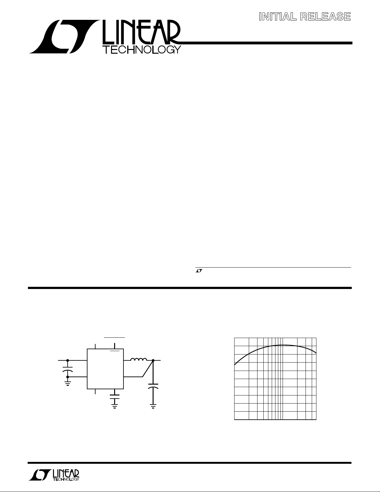
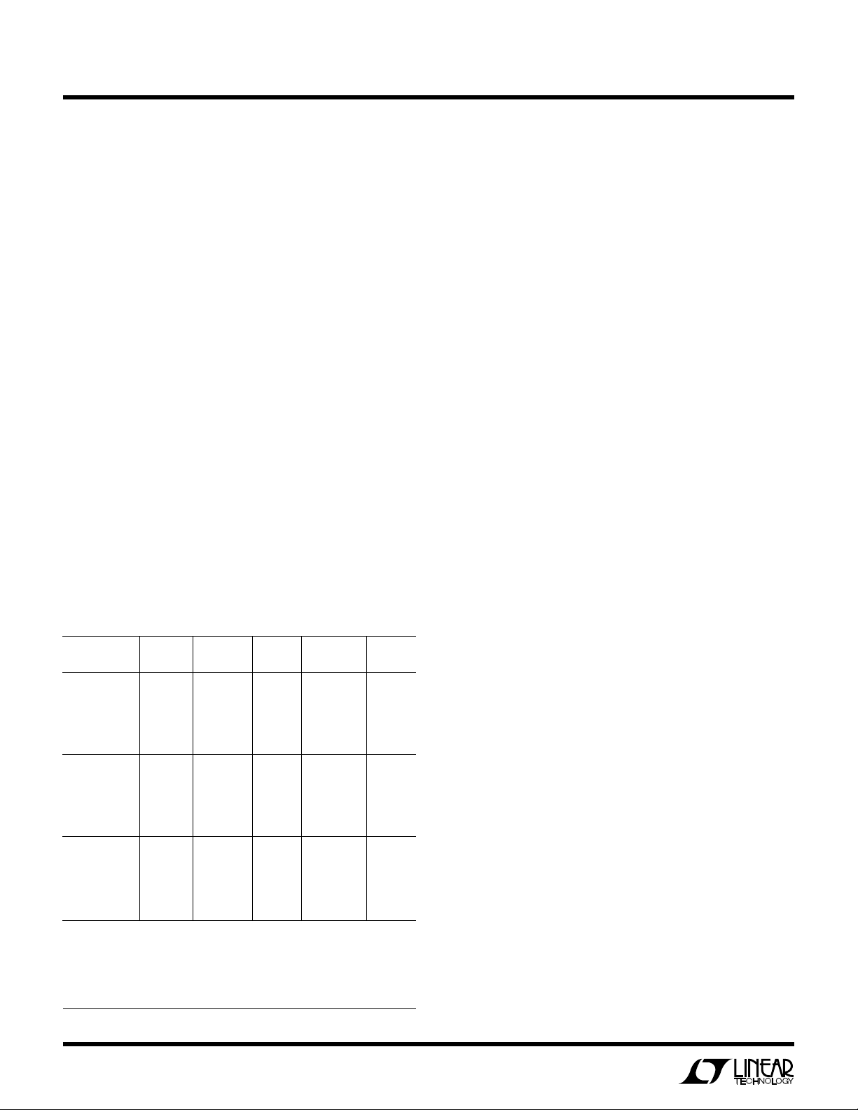
TYPICAL APPLICATION
The LTC®1504 is a self-contained, high efficiency synchronous buck switching regulator. It includes a pair of
on-chip 1.5Ω power switches, enabling it to supply up to
500mA of load current. Efficiency peaks at 92%, minimizing heat and wasted power. The synchronous buck architecture allows the output to source or sink current as
required to keep the output voltage in regulation.
The LTC1504 is available in adjustable and fixed 3.3V
output versions. An adjustable current limit circuit provides protection from overloads. The internal 1% reference combined with a sophisticated voltage feedback loop
provides optimum output voltage accuracy and fast load
transient response. The LTC1504 is specified to operate
with input voltages between 4V and 10V. Contact the LTC
factory for guaranteed specifications at 2.7V supply.
The LTC1504 is available in a plastic SO-8 package.
, LTC and LT are registered trademarks of Linear Technology Corporation.
Minimum Part Count 5V to 3.3V Regulator 5V to 3.3V Efficiency
5V
+
C
CIN: AVX TPSC226M016R0375
: AVX TAJC476M010
C
OUT
: COILTRONICS CTX50-1P
L
EXT
IN
SHUTDOWNNC
I
MAX
V
CC
LTC1504-3.3
GND
SS COMP
NC
100
90
SHDN
SENSE
Information furnished by Linear Technology Corporation is believed to be accurate and reliable.
However, no responsibility is assumed for its use. Linear Technology Corporation makes no representation that the interconnection of its circuits as described herein will not infringe on existing patent rights.
SW
1000pF
L
EXT
3.3V AT 500mA
+
C
OUT
1504 • TA01
80
70
60
50
40
EFFICIENCY (%)
30
20
10
0
10
LOAD CURRENT (mA)
100 500
1504 • TA02
1
Page 2
LTC1504
WU
U
PACKAGE
/
O
RDER I FOR ATIO
WW
W
U
ABSOLUTE MAXIMUM RATINGS
(Note 1)
Supply Voltage (VCC to GND)................................... 10V
Peak Output Current (SW) .......................................±1A
Input Voltage (All Other Pins) ......... –0.3V to VCC + 0.3V
Operating Temperature Range ..................... 0°C to 70°C
Storage Temperature Range ................. –65°C to 150°C
I
MAX
V
SW
GND
Lead Temperature (Soldering, 10 sec).................. 300°C
*FB FOR LTC1504CS8, SENSE FOR LTC1504CS8-3.3
Consult factory for Industrial and Military grade parts.
ELECTRICAL CHARACTERISTICS
SYMBOL PARAMETER CONDITIONS MIN TYP MAX UNITS
V
CC
V
FB
∆V
FB
V
SENSE
∆V
SENSE
I
CC
f
OSC
R
SW
V
IH
V
IL
I
IN
V
OH
V
OL
IOH, I
g
mV
A
V
g
mI
I
MAX
ISSSoft Start Source Current VSS = 0V ● –8 –12 –16 µA
tr, t
f
DC
MAX
Minimum Supply Voltage (Note 7) ● 4V
Feedback Voltage LTC1504CS8 ● 1.25 1.265 1.28 V
Feedback Voltage PSRR Figure 1, 4V ≤ VCC ≤ 10V, LTC1504CS8 ● 1.1 1.6 %
Sense Pin Voltage LTC1504CS8-3.3 ● 3.20 3.30 3.40 V
Sense Voltage PSRR Figure 1, 4V ≤ VCC ≤ 10V, LTC1504CS8-3.3 ● 1.2 1.8 %
Supply Current Figure 1, V
Figure 1, V
= 0V ● 1.0 20 µA
V
SHDN
Internal Oscillator Frequency ● 150 200 250 kHz
Internal Switch Resistance ● 1.3 2.0 Ω
SHDN Input High Voltage ● 2.4 V
SHDN Input Low Voltage ● 0.8 V
SHDN Input Current ● ±0.1 ±1 µA
Error Amplifier Positive Swing Figure 2 ● 4.5 4.95 V
Error Amplifier Negative Swing Figure 2 ● 0.05 0.5 V
Error Amplifier Output Current Figure 2 ● ±50 ±100 ±200 µA
OL
Error Amplifier Transconductance (Note 5) ● 350 600 1100 µmho
Error Amplifier DC Gain (Note 5) ● 40 48 dB
I
Amplifier Transconductance (Note 6) 1000 2000 3000 µmho
LIM
I
Sink Current V
MAX
Output Switch Rise/Fall Time ● 550 ns
Maximum Duty Cycle V
IMAX
COMP
= V
= V
VCC = 5V, TA = 25°C unless otherwise specified. (Note 2)
SHDN
SHDN
CC
CC
= VCC, I
= VCC, I
= 0 (Note 4) 3 mA
OUT
= 0, VFB/V
OUT
SENSE
TOP VIEW
1
2
CC
3
4
S8 PACKAGE
8-LEAD PLASTIC SO
T
= 115°C, θJA = 90°C/W
JMAX
= VCC (Note 4) ● 0.3 0.6 mA
COMP
8
SS
7
SHDN
6
FB/SENSE*
5
● 81216 µA
● 84 90 %
ORDER PART
NUMBER
LTC1504CS8
LTC1504CS8-3.3
S8 PART MARKING
1504
15043
2
Page 3
ELECTRICAL CHARACTERISTICS
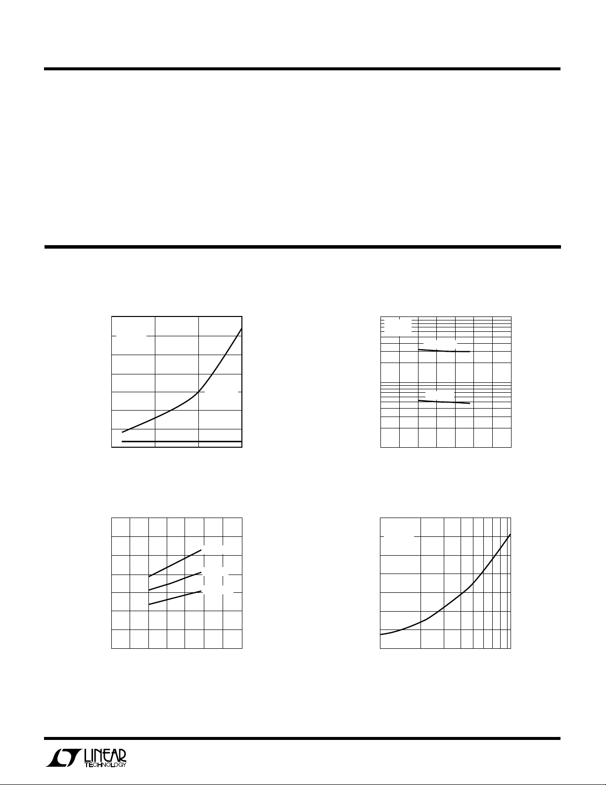
R
IMAX
(Ω)
10k
CURRENT LIMIT THRESHOLD (mA)
700
600
500
400
300
200
100
0
100k
1504 • TPC04
TA = 25°C
V
CC
= 5V
TEMPERATURE (°C)
–50 –25 0 25 50 75 100 125
SUPPLY CURRENT (mA)
10
1
0.1
1504 • TPC02
VFB = V
OUT
VFB = V
CC
VCC = 5V
I
OUT
= 0
LTC1504
The ● denotes specifications which apply over the full operating
temperature range.
Note 1: Absolute Maximum Ratings are those values beyond which the life
of the device may be impaired.
Note 2: All currents into device pins are positive; all currents out of device
pins are negative. All voltages are referenced to ground unless otherwise
specified.
Note 3: This parameter is guaranteed by correlation and is not tested
the output stage will stop switching and the static quiescent current can be
observed. With FB or SENSE hooked up normally, the output stage will be
switching and total dynamic supply current can be measured.
Note 5: Fixed output parts will appear to have g
lower than the specified values, due to the internal divider resistors.
Note 6: The I
(not current limited) operation, the I
Note 7: Contact factory for guaranteed specifications at 2.7V supply.
directly.
Note 4: LTC1504 quiescent current is dominated by the gate drive current
drawn by the onboard power switches. With FB or SENSE pulled to V
W
U
CC
TYPICAL PERFORMANCE CHARACTERISTICS
Supply Current vs Supply Voltage
14
TA = 25°C
= 0
I
OUT
12
10
8
6
VFB = V
OUT
and AV values 2.6 times
mV
amplifier can sink but not source current. Under normal
LIM
output current will be zero.
LIM
Supply Current vs Temperature
SUPPLY CURRENT (mA)
3.5
3.0
2.5
2.0
1.5
1.0
SWITCH ON-RESISTANCE (Ω)
0.5
4
2
0
2.5
VFB = V
CC
5
SUPPLY VOLTAGE (V)
Switch On-Resistance vs
Temperature
0
–50
–25 0
TEMPERATURE (°C)
50 100 125
25 75
7.5 10
1504 • TPC01
VCC = 3.3V
VCC = 5V
VCC = 10V
1504 • TPC03
Current Limit Threshold vs R
IMAX
3
Page 4
LTC1504
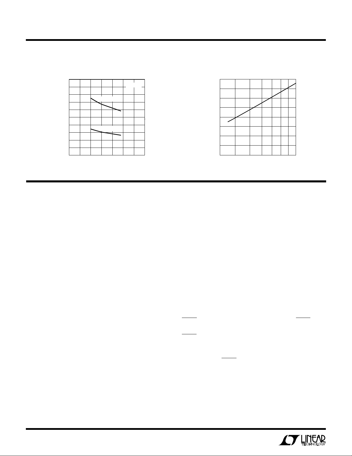
SUPPLY VOLTAGE (V)
357
SHUTDOWN PIN THRESHOLD (V)
4.0
3.5
3.0
2.5
2.0
1.5
1.0
0.5
0
10
1504 • TPC07
W
U
TYPICAL PERFORMANCE CHARACTERISTICS
Current Limit Threshold vs
Temperature
500
450
400
350
300
250
200
150
100
CURRENT LIMIT THRESHOLD (mA)
50
0
–50
PIN FUNCTIONS
I
(Pin 1): Current Limit Set. Connect a resistor from
MAX
VCC to I
12µA current source from I
drop across this resistor. This voltage is compared to the
voltage drop across the internal high-side switch (Q1)
while it is turned on. See the Applications Information
section for more information. To disable current limit,
leave I
VCC (Pin 2): Power Supply Input. Connect to a power
supply voltage between 4V and 10V. VCC requires a low
impedance bypass capacitor to ground, located as close
as possible to the LTC1504. See the Applications Information section for details on capacitor selection and
placement.
SW (Pin 3): Power Switch Output. This is the switched
node of the buck circuit. Connect SW to one end of the
external inductor. The other end of the inductor should be
connected to C
voltage. Avoid shorting SW to GND or VCC.
GND (Pin 4): Ground. Connect to a low impedance ground.
The input and output bypass capacitors and the feedback
resistor divider (adjustable parts only) should be grounded
as close to this pin as possible. Pin 4 acts as a heat sink
in the LTC1504 S0-8 package and should be connected to
4
to set the current limit threshold. An internal
MAX
floating.
MAX
OUT
VCC = 5V
R
= 47k
IMAX
R
= 22k
IMAX
–25 0 25 50 75
TEMPERATURE (°C)
100
1504 • TPC05
125
UUU
to GND sets the voltage
MAX
and becomes the regulated output
Shutdown Threshold vs
Supply Voltage
as large a copper area as possible to improve thermal
dissipation. See the Thermal Considerations section for
more information.
FB (LTC1504CS8) (Pin 5): Feedback. Connect FB to a
resistor divider from V
to GND to set the regulated
OUT
output voltage. The LTC1504CS8 feedback loop will servo
the FB pin to 1.265V.
SENSE (LTC1504CS8-3.3) (Pin 5): Output Voltage Sense.
Connect directly to the output voltage node. The
LTC1504CS8-3.3 feedback loop will servo SENSE to 3.3V.
SENSE is connected to an internal resistor divider which
will load any external dividers. For output voltages other
than 3.3V, use the LTC1504CS8.
SHDN (Pin 6): Shutdown, Active Low. When SHDN is at a
logic High, the LTC1504 will operate normally. When
SHDN is Low, the LTC1504 ceases all internal operation
and supply current drops below 1µ A. In shutdown, the SW
pin is pulled low. This ensures that the output is actively
shut off when SHDN is asserted, but it prevents other
supplies from providing power to the output when the
LTC1504 is inactive. See the Applications Information
section for more details.
SS (Pin 7): Soft Start. Connect an external capacitor
(usually 0.1µ F) from SS to GND to limit the output rise time
Page 5

UUU
PIN FUNCTIONS
LTC1504
during power-up. CSS also compensates the current limit
loop, allowing the LTC1504 to enter and exit current limit
cleanly. See the Applications Information section for more
details.
W
BLOCK DIAGRAM
SHDN
COMP
SAW
12V
SS
I
LIM
–+
TO INTERNAL BLOCKS
–
+
FB
+–
PWM
MIN
+–
COMP (Pin 8): External Compensation. An external RC
network should be connected to COMP to compensate the
feedback loop. COMP is connected to the output of the
internal error amplifier.
V
CC
Q1
SW
Q2
MAX
+–
I
MAX
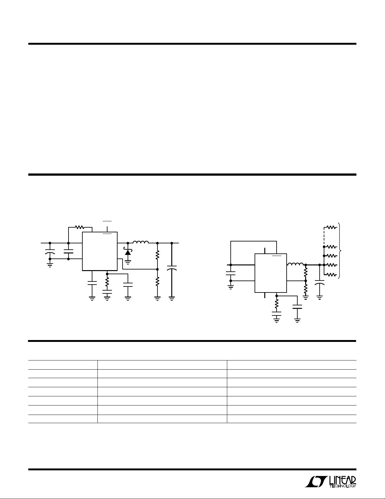
TEST CIRCUITS
V
CC
+
C
IN
CIN: AVX TPSE107M016R0125
: SANYO 16CV220GX
C
OUT
: COILCRAFT D03316-473
L
EXT
1µF
12V
NC
I
SHDN
MAX
V
CC
LTC1504
GNDSWFB/SENSE
SS COMP
0.1µF
Figure 1
7.5k
0.01µF
FB
20.4k
12.6k
(ADJ ONLY)
SENSE
(–3.3V ONLY)
1504 • BD
–
+
40mV
V
REF
+
–
1.265V
+
40mV
–
Figure 3. Block Diagram
V
REF
A: TEST V
B: TEST V
LTC1504
–
+
, IOL
OL
, I
OH
OH
COMP
1504 • TC02
L
EXT
+
220pF
V
OUT
C
OUT
1504 • TC01
A
FB/SENSE
B
Figure 2
5
Page 6

LTC1504
U
WUU
APPLICATIONS INFORMATION
OVERVIEW
The LTC1504 is a complete synchronous switching regulator controller (see Block Diagram). It includes two
on-chip 1.5Ω power MOSFETs, eliminating the need for
external power devices and minimizing external parts
count. The internal switches are set up as a synchronous
buck converter with a P-channel device (Q1) from the
input supply to the switching node and an N-channel
device (Q2) as the synchronous rectifier device from the
switching node to ground. An external inductor, input and
output bypass capacitors and the compensation network
complete the control loop. The LTC1504 adjustable output
parts require an additional pair of resistors to set the
output voltage. The LTC1504-3.3 parts include an onboard
resistor divider preset to a 3.3V output voltage. A functional 3.3V output regulator can be constructed with an
LTC1504-3.3 and as few as four external components.
The LTC1504 feedback loop includes a precision reference
trimmed to 1% (V
feedback amplifier (FB) and an onboard PWM generator
(SAW and PWM). Two additional feedback comparators
(MIN and MAX) monitor the feedback voltage and override
the primary feedback amplifier when the regulated out falls
outside a ±3% window, improving transient response.
The internal sawtooth oscillator typically runs at 200kHz.
Q1 and Q2 are capable of carrying peak currents in excess
of 500mA, with the continuous output power level limited
primarily by the thermal dissipation of the SO-8 package.
With a 5V input and a 3.3V output, the LTC1504 can supply
500mA of continuous output current with an appropriate
layout. An on-chip current limit circuit, set with a single
external resistor, can be used to help limit power dissipation. See the Thermal Considerations section for more
information.
Theory of Operation
The LTC1504 primary feedback loop consists of the main
error amplifier FB, the PWM generator, the output drive
logic and the power switches. The loop is closed with the
external inductor and the output bypass capacitor. The
feedback amplifier senses the output voltage directly at the
SENSE pin for fixed output versions or through an external
), a wide bandwidth transconductance
REF
resistor divider in the adjustable output version. This
feedback voltage is compared to the 1.265V internal
reference voltage by FB and an error signal is generated at
the COMP pin. COMP is a high impedance node that is
brought out to an external pin for optimizing the loop
compensation.
COMP is compared to a 200kHz sawtooth wave by comparator PWM. This raw pulse-width modulated signal is
logically combined with the outputs of the transient comparators MIN and MAX before reaching the output stage.
The output stage generates nonoverlapping drive for the
onboard P- and N-channel power MOSFETs, which drive
the SW pin with a low impedance image of the PWM
waveform. Typical open-loop output impedance at SW is
between 1Ω and 3Ω, depending on supply voltage. This
high power pulse train is filtered by the external inductor
and capacitor, providing a steady DC value at the output
node. This node returns to FB or SENSE, closing the loop.
The MIN and MAX comparators in the feedback loop
provide high speed fault correction in situations where the
FB amplifier may not respond quickly enough. MIN compares the feedback signal to a voltage 40mV (3%) below
the internal reference. At this point, MIN overrides the FB
amplifier and forces the loop to full duty cycle. Similarly,
MAX monitors the output voltage at 3% above the internal
reference and forces the output to 0% duty cycle when
tripped. These two comparators prevent extreme output
perturbations with fast output transients, while allowing
the main feedback loop to be optimally compensated for
stability.
The LTC1504 includes yet another feedback loop that
controls operation in current limit. The I
monitors the voltage at the SW pin while Q1 is on. It
compares this voltage to the voltage at the I
peak current through Q1 rises, the voltage drop across it
due to its RON increases proportionally. When SW drops
below I
creased beyond the desired value, I
controlled amount of current out of SS, the external soft
start pin. As SS falls, it pulls COMP down with it, limiting
the duty cycle and reducing the output voltage to control
the current. The speed at which the current limit circuit
reacts is set by the value of the external soft start capacitor.
, indicating the current through Q1 has in-
MAX
LIM
amplifier
LIM
pin. As the
MAX
starts pulling a
6
Page 7

LTC1504
U
WUU
APPLICATIONS INFORMATION
EXTERNAL COMPONENT SELECTION
External components required by the LTC1504 fall into
three categories: input bypass, output filtering and compensation. Additional components to set up soft start and
current limit are usually included as well. A minimum
LTC1504 circuit can be constructed with as few as four
external components; a circuit that utilizes all of the
LTC1504s functionality usually includes eight or nine
external components, with two additional feedback resistors required for adjustable parts. See the Typical Applications section for examples of external component hookup.
Input Bypass
The input bypass capacitor is critical to proper LTC1504
operation. The LTC1504 includes a precision reference
and a pair of high power switches feeding from the same
VCC pin. If VCC does not have adequate bypassing, the
switch pulses introduce enough ripple at VCC to corrupt
the reference voltage and the LTC1504 will not regulate
accurately. Symptoms of inadequate bypassing include
poor load regulation and/or erratic waveforms at the SW
pin. If an oscilloscope won’t trigger cleanly when looking
at the SW pin, there isn’t adequate input bypass.
Ideally, the LTC1504 requires a low impedance bypass
right at the chip and a larger reservoir capacitor that can be
located somewhat farther away. This requirement usually
can be met with a ceramic capacitor right next to the
LTC1504 and an electrolytic capacitor (usually 10µF to
100µF, depending on expected load current) located some-
where nearby. In certain cases, the bulk capacitance
requirement can be met by the output bypass of the input
supply. Applications running at very high load currents or
at input supply voltages greater than 6V may require the
local ceramic capacitor to be 1µF or greater. In some
cases, both the low impedance and bulk capacitance
requirements can be met by a single capacitor, mounted
very close to the LTC1504. Low ESR organic semiconductor (OS-CON) electrolytic capacitors or surge tested surface mount tantalum capacitors can have low enough
impedance to keep the LTC1504 happy in some circuits.
Often the RMS current capacity of the input bypass capacitors is more important to capacitor selection than value.
Buck converters like the LTC1504 are hard on input
capacitors, since the current flow alternates between the
full load current and near zero during every clock cycle. In
the worst case (50% duty cycle or V
= 0.5VIN) the RMS
OUT
current flow in the input capacitor is half of the total load
current plus half the ripple current in the inductor—
perhaps 300mA in a typical 500mA load current application. This current flows through the ESR of the input
bypass capacitor, heating it up and shortening its life,
sometimes dramatically. Many ordinary electrolytic capacitors that look OK at fist glance are not rated to
withstand such currents—check the RMS current rating
before you specify a device! If the RMS current rating isn’t
specified, it should not be used as an input bypass
capacitor. Again, low ESR electrolytic and surge tested
tantalums usually do well in LTC1504 applications and
have high RMS current ratings. The local ceramic bypass
capacitor usually has negligible ESR allowing it to withstand large RMS currents without trouble. Table 1 shows
typical surface mount capacitors that make acceptable
input bypass capacitors in LTC1504 applications.
Table 1. Representative Surface Mount Input Bypass Capacitors
PART VALUE ESR MAX RMS TYPE HEIGHT
AVX
TPSC226M016R0375 22µF 0.38Ω 0.54A Tantalum 2.6mm
TPSD476M016R0150 47µF 0.15Ω 0.86A Tantalum 2.9mm
TPSE107M016R0125 100µF 0.13Ω 1.15A Tantalum 4.1mm
1206YC105M 1µF Low >1A X7R Ceramic 1.5mm
1210YG106Z 10µF Low >1A Y5V Ceramic 1.7mm
Sanyo
16SN33M 33µF 0.15Ω 1.24A OS-CON 7mm
16SN68M 68µF 0.1Ω 1.65A OS-CON 7mm
16CV100GX 100µF 0.44Ω 0.23A* Electrolytic 6mm
16CV220GX 220µF 0.34Ω 0.28A* Electrolytic 7.7mm
Sprague
593D476X0016D2W 47µF 0.17Ω 0.93A Tantalum 2.8mm
593D107X0016E2W 100µ 0.15Ω 1.05A Tantalum 4mm
*Note: Use multiple devices in parallel or limit output current to prevent capacitor overload.
Inductor
The LTC1504 requires an external inductor to be connected from the switching node SW to the output node
where the load is connected. Inductor requirements are
fairly straightforward; it must be rated to handle continuous DC current equal to the maximum load current plus
7
Page 8
LTC1504
U
WUU
APPLICATIONS INFORMATION
half the ripple current and its value should be chosen
based on the desired ripple current and/or the output
current transient requirements. Large value inductors
lower ripple current and decrease the required output
capacitance, but limit the speed that the LTC1504 can
change the output current, limiting output transient response. Small value inductors result in higher ripple
currents and increase the demands on the output capacitor, but allow faster output current slew rates and are often
smaller and cheaper for the same DC current rating. A
typical inductor used in an LTC1504 application might
have a maximum current rating between 500mA and 1A
and an inductance between 33µH and 220µH.
Different core materials and shapes will change the size/
current and price/current relationship of an inductor. Toroid
or shielded pot cores in ferrite or permalloy materials are
small and don’t radiate much energy, but generally cost more
than powdered iron rod core inductors with similar electrical
characteristics. The choice of which style inductor to use
often depends more on the price vs size requirements and any
radiated field/EMI requirements than on what the LTC1504
requires to operate. Table 2 shows some typical surface
mount inductors that work well in LTC1504 applications.
Table 2. Representative Surface Mount Inductors
CORE CORE
PART VALUE MAX DC TYPE MATERIAL HEIGHT
CoilCraft
DT3316-473 47µH 1A Shielded Ferrite 5.1mm
DT3316-104 100µH 0.8A Shielded Ferrite 5.1mm
DO1608-473 47µH 0.5A Open Ferrite 3.2mm
DO3316-224 220µH 0.8A Open Ferrite 5.5mm
Coiltronics
CTX50-1 50µH 0.65A Toroid KoolMµ
CTX100-2 100µH 0.63A Toroid KoolMµ 6mm
CTX50-1P 50µH 0.66A Toroid Type 52 4.2mm
CTX100-2P 100µH 0.55A Toroid Type 52 6mm
Sumida
CDRH62-470 47µH 0.54A Shielded Ferrite 3mm
CDRH73-101 100µH 0.50A Shielded Ferrite 3.4mm
CD43-470 47µH 0.54A Open Ferrite 3.2mm
CD54-101 100µH 0.52A Open Ferrite 4.5mm
Output Capacitor
The output capacitor affects the performance of the
LTC1504 in a couple of ways: it provides the first line of
Kool Mµ is a registered trademark of Magnetics, Inc..
®
4.2mm
defense during a transient load step and it has a large effect
on the compensation required to keep the LTC1504 feedback loop stable. Transient load response of an LTC1504
circuit is controlled almost entirely by the output capacitor
and the inductor. In steady load operation, the average
current in the inductor will match the load current. When
the load current changes suddenly, the inductor is suddenly carrying the wrong current and requires a finite
amount of time to correct itself—at least several switch
cycles with typical LTC1504 inductor values. Even if the
LTC1504 had psychic abilities and could instantly assume
the correct duty cycle, the rate of change of current in the
inductor is still related to its value and will not change
instantaneously.
Until the inductor current adjusts to match the load current, the output capacitor has to make up the difference.
Applications that require exceptional transient response
(2% or better for instantaneous full-load steps) will require relatively large value, low ESR output capacitors.
Applications with more moderate transient load requirements can often get away with traditional standard ESR
electrolytic capacitors at the output and can use larger
valued inductors to minimize the required output capacitor value. Note that the RMS current in the output capacitor
is slightly more than half of the inductor ripple current—
much smaller than the RMS current in the input bypass
capacitor. Output capacitor lifetime is usually not a factor
in typical LTC1504 applications.
Large value ceramic capacitors used as output bypass
capacitors provide excellent ESR characteristics but can
cause loop compensation difficulties. See the Loop Compensation section.
Loop Compensation
Loop compensation is strongly affected by the output
capacitor. From a loop stability point of view, the output
inductor and capacitor form a series RLC resonant circuit,
with the L set by the inductor value, the C by the value of
the output capacitor and the R dominated by the output
capacitor’s ESR. The amplitude response and phase shift
due to these components is compensated by a network of
Rs and Cs at the COMP pin to (hopefully) close the
feedback loop in a stable manner. Qualitatively, the L and
8
Page 9

LTC1504
U
WUU
APPLICATIONS INFORMATION
C of the output stage form a 2nd order roll-off with 180° of
phase shift; the R due to ESR forms a single zero at a
somewhat higher frequency that reduces the roll-off to
first order and reduces the phase shift to 90°.
If the output capacitor has a relatively high ESR, the zero
comes in well before the initial phase shift gets all the way
to 180° and the loop only requires a single small capacitor
from COMP to GND to remain stable (Figure 4a). If, on the
other hand, the output capacitor is a low ESR type to
maximize transient response, the ESR zero can increase in
frequency by a decade or more and the output stage phase
shift can get awfully close to 180° before it turns around
and comes back to 90°. Large value ceramic, OS-CON
electrolytic and low impedance tantalum capacitors fall
into this category. These loops require an additional zero
to be inserted at the COMP pin; a series RC in parallel with
a smaller C to ground will usually ensure stability. Figure
4b shows a typical compensation network which will
optimize transient response with most output capacitors.
Adjustable output parts can add a feedforward capacitor
across the feedback resistor divider to further improve
phase margin. The typical applications in this data sheet
V
OUT
R
*
LTC1504
Figure 4a. Minimum Compensation Network
LTC1504
R
Figure 4b. Optimum Compensation Network
FB
COMP
C
C
*ADJUSTABLE PARTS ONLY
FB
COMP
C
C
C
C
FB1
R
*
FB2
1504 • F04a
V
OUT
R
*
FB1
R
FB2
F
*ADJUSTABLE PARTS ONLY
CFF*
*
1504 • F04b
show compensation values that work with several combinations of external components—use them as a starting
point. For complex cases or stubborn oscillations, contact
the LTC Applications Department.
External Schottky Diode
An external Schottky diode can be included across the
internal N-channel switch (Q2) to improve efficiency at
heavy loads. The diode carries the inductor current during
the nonoverlap time while the LTC1504 turns Q1 off and
Q2 on and prevents current from flowing in the intrinsic
body diode in parallel with Q2. This diode will improve
efficiency by a percentage point or two as output current
approaches 500mA and can help minimize erratic behavior at very high peak current levels caused by excessive
parasitic current flow through Q2. A Motorola MBRS0530L
is usually adequate, with the cathode connected to SW and
the anode connected to GND. Note that this diode is not
required for normal operation and has a negligible effect
on efficiency at low (< 250mA) output currents.
Soft Start and Current Limit
Soft start and current limit are linked in the LTC1504. Soft
start works in a straightforward manner. An internal 12µ A
current source connected to the SS pin will pull up an
external capacitor connected from SS to GND at a rate
determined by the capacitor value. COMP is clamped to a
voltage one diode drop above SS; as SS rises, COMP will
rise at the same rate. When COMP reaches roughly 2V
below VCC, the duty cycle will slowly begin to increase until
the output comes into regulation. As SS continues to rise,
the feedback amplifier takes over at COMP, the clamp
releases and SS rises to VCC. During a soft start cycle, the
MIN feedback comparator is disabled to prevent it from
overriding the COMP pin and forcing the output to maximum duty cycle.
Current limit operates by pulling down on the soft start pin
when it senses an overload condition at the output. The
current limit amplifier (I
) compares the voltage drop
LIM
across the internal P-channel switch (Q1) during its on
time to the voltage at the I
MAX
pin. I
includes an internal
MAX
12µA pull-down, allowing the voltage to be set by a single
resistor between VCC and I
. When the IR drop across
MAX
9
Page 10
LTC1504
U
WUU
APPLICATIONS INFORMATION
Q1 exceeds the drop across the I
current out of the external soft start capacitor, reducing the
voltage at SS. A soft start capacitor should always be used
if current limit is enabled. SS, in turn, pulls down on COMP,
limiting the output duty cycle and controlling the output
current. When the current overload is removed, the I
amplifier lets go of SS and allows it to rise again as if it were
completing a soft start cycle. The size of the external soft
start capacitor controls both how fast the current limit
responds once an overload is detected and how fast the
output recovers once the overload is removed. The soft
start capacitor also compensates the feedback loop created by the I
feedback loop, the additional phase shift due to the output
inductor and capacitor do not come into play and the loop
can be adequately compensated with a single capacitor.
Usually a 0.1µF ceramic capacitor from SS to GND pro-
vides adequate soft start behavior and acceptable current
limit response.
This type of current limit circuit works well with mild
current overloads and eliminates the need for an external
current sensing resistor, making it attractive for LTC1504
applications. These same features also handicap the current limit circuit under severe short circuits when the
output voltage is very close to ground. Under this condition, the LTC1504 must run at extremely narrow duty
cycles (<5%) to keep the current under control. When the
on-time falls below the time required to sense the current
in Q1, the LTC1504 responds by reducing the oscillator
frequency, increasing the off-time to decrease the duty
cycle and allow it to maintain some control of the output
current. The oscillator frequency may drop by as much as
a factor of 10 under severe current overloads.
Under extreme short circuits (e.g., screwdriver to ground)
the on-time will reduce to the point where the LTC1504 will
lose control of the output current. At this point, output
current will rise until the inductor saturates, and the
current will be limited by the parasitic ESL of the inductor
and the RON of Q2 inside the LTC1504. This current is
usually nondestructive and dissipates a limited amount of
power since the output voltage is very low. A typical
LTC1504 circuit can withstand such a short for many
seconds without damage. The test circuit in Figure 1 will
amplifier. Because the I
LIM
resistor, I
MAX
LIM
pulls
LIM
LIM
loop is a current
typically withstand a direct output short for more than 30
seconds without damage to the LTC1504. Eventually,
however, a continuous short may cause the die temperature to rise to destructive levels.
Note that the current limit is primarily designed to protect
the LTC1504 from damage and is not intended to be used
to generate an accurate constant-current output. As the
die temperature varies in a current limited condition, the
RON of the internal switches will change and the current
limit threshold will move around. RON will also vary from
part-to-part due to manufacturing tolerance. The external
I
resistor should be chosen to allow enough room to
MAX
account for these variations without allowing the current
limit to engage at the maximum expected load current. A
current limit setting roughly double the expected load is
often a good compromise, eliminating unintended current
limit operation while preventing circuit destruction under
actual fault conditions. If desired, current limit can be
disabled by floating the I
will pull I
Shutdown
The LTC1504 includes a micropower shutdown mode
controlled by the logic level at SHDN. A logic High at SHDN
allows the part to operate normally. A logic Low at SHDN
stops all internal switching, pulls COMP, SS and SW to
GND and drops quiescent current below 1µA typically.
Note that the internal N-channel power MOSFET from SW
to GND turns on when SHDN is asserted. This ensures that
the output voltage drops to zero when the LTC1504 is shut
down, but prevents other devices from powering the
output when the LTC1504 is disabled.
External Clock Synchronization
The LTC1504 SHDN pin can double as an external clock
input for applications that require a synchronized clock or
a faster switching speed. The SHDN pin terminates the
internal sawtooth wave and resets the oscillator immediately when it goes low, but waits 50µs before shutting
down the rest of the internal circuitry. A clock signal
applied directly to the SHDN pin will force the LTC1504
internal oscillator to lock to its frequency as long as the
external clock runs faster than the internal oscillator
to GND and the I
MAX
pin; the internal current source
MAX
amplifier will be disabled.
LIM
10
Page 11

LTC1504
U
WUU
APPLICATIONS INFORMATION
frequency. Attempting to synchronize to a frequency
lower than the 250kHz maximum internal frequency may
result in inconsistent pulse widths and is not recommended.
Because the sawtooth waveform rises at a fixed rate
internally, terminating it early by synchronizing to a fast
external clock will reduce the amplitude of the sawtooth
wave that the PWM comparator sees, effectively raising
the gain from COMP to SW. 500kHz is the maximum
recommended synchronization frequency; higher frequencies will reduce the sawtooth amplitude to the point that
the LTC1504 may run erratically.
THERMAL CONSIDERATIONS
Each of the LTC1504 internal power switches has approximately 1.5Ω of resistance at room temperature and will
happily carry more than the rated maximum current if the
current limit is set very high or is not connected. Since the
inductor current is always flowing through one or the
other of the internal switches, a typical application supplying 500mA of load current will cause a continuous dissipation of approximately 375mW. The SO-8 package has a
thermal resistance of approximately 90°C/W, meaning
that the die will begin to rise toward 34°C above ambient
at this power level. The RON of the internal power switches
increases as the die temperature rises, increasing the
power dissipation as the feedback loop continues to keep
the output current at 500mA. At high ambient temperatures, this cycle may continue until the chip melts, since
the LTC1504 does not include any form of thermal shutdown. Applications can safely draw peak currents above
the 500mA level, but the average power dissipation should
be carefully calculated so that the maximum 115°C die
temperature is not exceeded.
The LTC1504 dissipates the majority of its heat through its
pins, especially GND (Pin 4). Thermal resistance to ambient can be optimized by connecting GND to a large copper
region on the PCB, which will serve as a heat sink.
Applications which will operate the LTC1504 near maximum power levels or which must withstand short circuits
of extended duration should maximize the copper area at
all pins and ensure that there is some airflow over the part
to carry away excess heat. For layout assistance in situa-
tions where power dissipation may be a concern, contact
the LTC Applications Department.
The current limit circuit can be used to limit the power
under mild overloads to a safe level, but severe overloads
where the output is shorted to ground may still cause the die
temperature to rise dangerously. For more information on
current limit behavior, see the Current Limit section.
LAYOUT CONSIDERATIONS
Like all precision switching regulators, the LTC1504
requires special care in layout to ensure optimum performance. The large peak currents coupled with significant
DC current flow will conspire to keep the output from
regulating properly if the layout is not carefully planned. A
poorly laid out op amp or data converter circuit will fail to
give the desired performance, but will usually still act like
an op amp or data converter. A poorly laid out LTC1504
circuit may look nothing at all like a regulator.
or plug-in prototyping boards are not useful for breadboarding LTC1504 circuits!
Perhaps most critical to proper LTC1504 performance is
the layout of the ground node and the location of the input
and output capacitors. The negative terminals of both the
input and output bypass capacitors should come together
at the same point, as close as possible to the LTC1504
ground pin. The compensation network and soft start
capacitor can be connected together on their own trace,
which should come directly back to this same common
ground point. The input supply ground and the load return
should also connect to this common point. Each ground
line should come to a star connection with Pin 4 at the
center of the star. This node should be a fairly large copper
region to act as a heat sink if required.
Second in importance is the proximity of the low ESR (usually
ceramic) input bypass capacitor. It should be located as close
to the LTC1504 VCC and GND pins as physically possible.
Ideally, the capacitor should be located right next to the
package, straddling the SW pin. High peak current applications or applications with VCC greater than 6V may require a
1µ F or larger ceramic capacitor in this position.
One node that isn’t quite so critical is SW. Extra lead length
or narrow traces at this pin will only add parasitic induc-
Wire-wrap
11
Page 12
LTC1504
U
WUU
APPLICATIONS INFORMATION
tance in series with the external inductor, slightly raising
its value. The SW trace need only be wide enough to
support the maximum peak current under short circuit
conditions—perhaps 1A. If a trace needs to be compromised to make the layout work, this is the one. Note that
long traces at the SW node may aggravate EMI considerations—don’t get carried away. If a Schottky diode is used
at the SW node, it should be located at the LTC1504 end
of the trace, close to the device pins.
The LTC Applications Department has constructed literally hundreds of layouts for the LTC1504 and related
U
TYPICAL APPLICATIONS
High Efficiency 5V to 2.5V Converter with Current Limit
R
*
IMAX
V
CC
5V
+
CIN: AVX TPSE107M016R0125
: SANYO 16CV220GX
C
OUT
: COILCRAFT DO3316-473
L
EXT
*SELECT R
IMAX
1µF
C
IN
0.1µF
VALUE USING CURRENT LIMIT THRESHOLD GRAPH ON PAGE 3
I
MAX
V
CC
LTC1504
GND
SS COMP
SHDN
SHDN
SW
FB
7.5k
0.01µF
L
EXT
MBRS0530L
220pF
11.8k
12.1k
V
OUT
2.5V
+
C
OUT
1504 • TA03
parts, many of which worked and some of which are now
archived in the Bad Layout Hall of Fame. If you need layout
assistance or you think you have a candidate layout for the
Hall of Fame, give Applications a call at (408) 954-8400.
Demo boards with properly designed layouts are available
and specialized layouts can be designed if required. The
applications team is also experienced in external component selection for a wide variety of applications, and they
have a never-ending selection of tall tales to tell as well.
When in doubt, give them a call.
SCSI-2 Active Terminator
110Ω
•
•
•
110Ω
110Ω
110Ω
110Ω
C
OUT
1504 • TA04
18
TO
27
LINES
TERMPWR
C
: AVX TPSC107M006R0150
OUT
: SUMIDA CD54-470
L
EXT
4.7µF
CERAMIC
NC
I
MAX
V
CC
LTC1504
GND
SS COMP
NC
SHDN
SW
FB
7.5k
0.01µF
L
EXT
15k
+
12k
220pF
RELATED PARTS
PART NUMBER DESCRIPTION COMMENTS
LTC1174 600mA, High Efficiency Step-Down Converter Nonsynchronous, Better Low Load Efficiency
LT®1307 Single Cell 600kHz DC/DC Converter Boost Mode, Micropower
LT1372 1.5A, 500kHz Step-Up Switching Regulator Boost Mode, High Power
LT1376 1.5A, 500kHz Step-Down Switching Regulator Nonsynchronous, 1.5A Max Current
LTC1433/LTC1434 450mA, Low Noise Current Mode Step-Down Converters Nonsynchronous, Better Low Load Efficiency
LT1507 1.5A, 500kHz Monolithic Buck Regulator Nonsynchronous, 1.5A Max Current
1504i LT/TP 0897 4K • PRINTED IN USA
LINEAR TECHNOLOGY CORPORATION 1997
12
Linear Technology Corporation
1630 McCarthy Blvd., Milpitas, CA 95035-7417 ● (408) 432-1900
FAX: (408) 434-0507
●
TELEX: 499-3977 ● www.linear-tech.com
 Loading...