

Page 1
1
LTC1503-1.8/LTC1503-2
High Efficiency Inductorless
Step-Down DC/DC Converters
■
Input Voltage Range: 2.4V to 6V
■
Fixed Output Voltages: 1.8V ±4%, 2V ±4%
■
Output Current: Up to 100mA
■
No Inductors
■
Typical Efficiency 25% Higher than LDOs
■
Low Operating Current: 25µA
■
Low Shutdown Current: 5µA
■
600kHz Switching Frequency
■
Shutdown Disconnects Load from V
IN
■
Soft-Start Limits Inrush Current at Turn-On
■
Short-Circuit and Overtemperature Protected
■
Available in 8-Pin MSOP and SO Packages
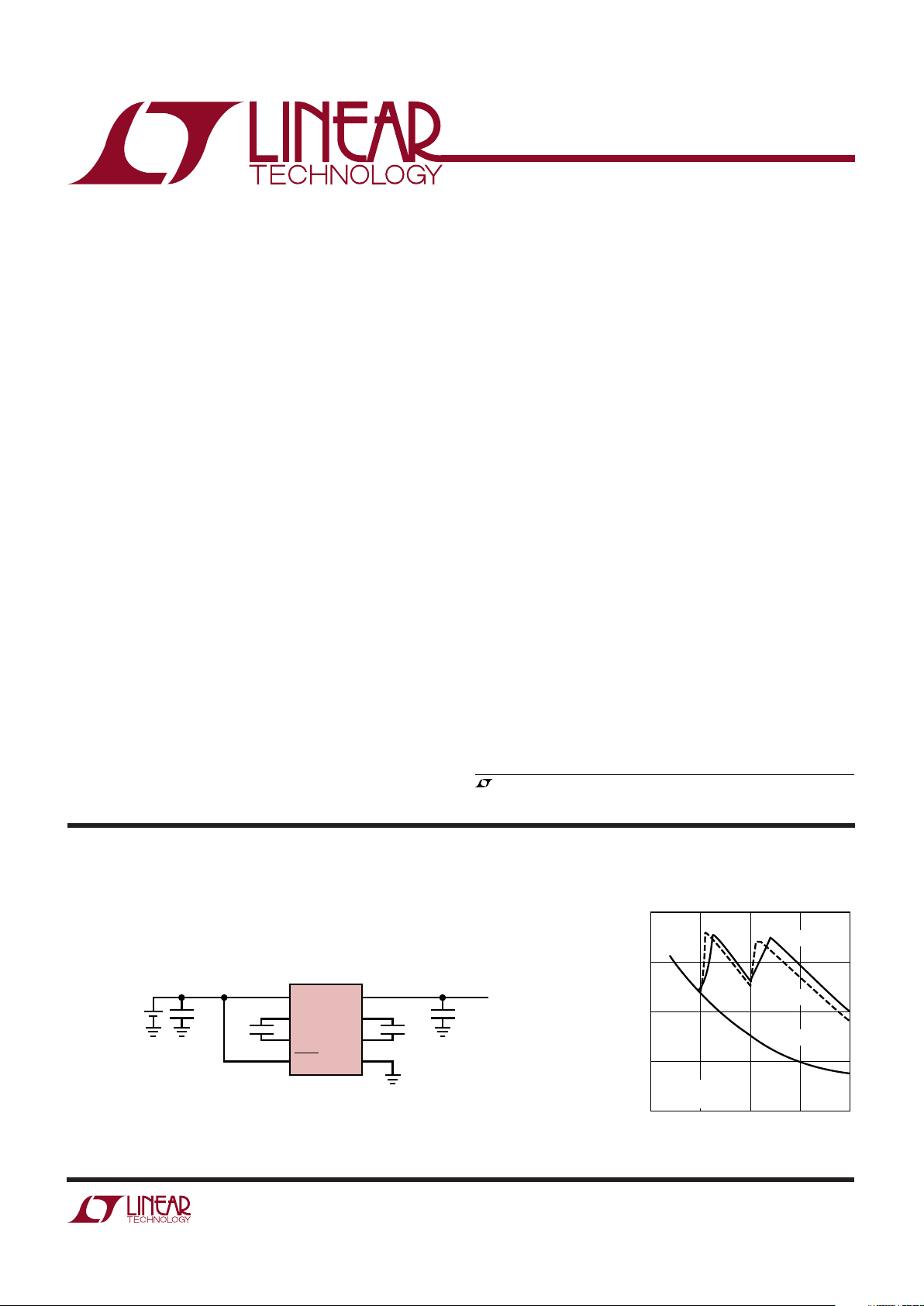
The LTC®1503-1.8/LTC1503-2 are switched capacitor
step-down DC/DC converters that produce a regulated
output from a 2.4V to 6V input. The parts use switched
capacitor fractional conversion to achieve high efficiency
over the entire input range. No inductors are required.
Internal circuitry controls the step-down conversion ratio
to optimize efficiency as the input voltage and load conditions vary. Typical efficiency is 25% higher than that of a
low dropout (LDO) linear regulator.
Regulation is achieved by sensing the output voltage and
enabling the internal switching network as needed to
maintain a fixed output voltage. This method of regulation
enables the parts to achieve high efficiency at extremely
light loads. Low operating current (25µA with no load, 5µA
in shutdown) and low external parts count (two 1µF flying
capacitors and two 10µF bypass capacitors) make the
LTC1503-1.8/LTC1503-2
ideally suited for space constrained battery-powered applications. The parts are fully
short-circuit and overtemperature protected.
The
LTC1503-1.8/
LTC1503-2 are available in 8-pin MSOP
and SO packages.
, LTC and LT are registered trademarks of Linear Technology Corporation.
■
Cellular Phones
■
Handheld Computers
■
Smart Card Readers
■
Low Power DSP Supplies
■
Portable Electronic Equipment
■
Handheld Medical Instruments
Efficiency vs Input Voltage
Single Li-Ion to 2V DC/DC Converter
FEATURES
DESCRIPTIO
U
APPLICATIO S
U
TYPICAL APPLICATIO
U
4
2
3
5
1
8
6
7
V
IN
C1
–
C1
+
SHDN/SS
V
OUT
C2
–
C2
+
GND
LTC1503-2
1µF
1503-1.8/2 TA01
1µF
10µF
1-CELL Li-Ion OR
3-CELL NiMH
10µF
V
OUT
= 2V
I
OUT
= 100mA
INPUT VOLTAGE (V)
2
EFFICIENCY (%)
60
80
6
1503-1.8/2 TA02
40
20
3
4
5
100
LTC1503-2
V
OUT
= 2V
I
OUT
= 100mA
I
OUT
= 1mA
“IDEAL” LDO
Page 2
2
LTC1503-1.8/LTC1503-2
Industrial Temperature Range ............... –40°C to 85°C
Specified Temperature Range (Note 2)... – 40°C to 85°C
Storage Temperature Range ................ –65°C to 150°C
Lead Temperature (Soldering, 10 sec)................. 300°C
(Note 1)
PARAMETER CONDITIONS MIN TYP MAX UNITS
VIN Operating Voltage ● 2.4 6 V
V
OUT
LTC1503-1.8, 0mA < I
OUT
< 100mA ● 1.728 1.8 1.872 V
LTC1503-2, 0mA < I
OUT
< 100mA ● 1.920 2.0 2.080 V
VIN Operating Current I
OUT
= 0mA ● 25 50 µA
VIN Shutdown Current SHDN/SS = 0V ● 510 µA
Output Ripple Voltage LTC1503-X, VIN = 3.6V, I
OUT
= 100mA 25 mV
P-P
Efficiency LTC1503-2, VIN = 3.6V, I
OUT
= 100mA 82.9 %
Switching Frequency Oscillator Free Running 600 kHz
SHDN/SS Input Threshold ● 0.2 0.35 0.5 V
SHDN/SS Input Current V
SHDN/SS
= 0V (Note 3) ● –3.5 –2 –1 µA
V
SHDN/SS
= V
IN
● –1 1 µA
V
OUT
Short-Circuit Current V
OUT
= 0V (Note 4) ● 82250 mA
V
OUT
Turn-On Time CSS = 0nF, VIN = 3.6V, C
OUT
= 10µF 0.1 ms
C
SS
= 10nF 8 ms
Note 1: Absolute Maximum Ratings are those values beyond which the life
of a device may be impaired.
Note 2: The LTC1503C is guaranteed to meet specified performance from
0°C to 70°C and is designed, characterized and expected to meet these
extended temperature limits, but are not tested at –40°C and 85°C. The
LTC1503I is guaranteed to meet the extended temperature limits.
Note 3: Currents flowing into the device are positive polarity. Currents
flowing out of the device are negative polarity.
Note 4: When V
OUT
is less than 150mV, I
OUT
is limited to much less than
the maximum rated output current to prevent damage to the output
devices.
ORDER PART
NUMBER
LTC1503CMS8-1.8
LTC1503CMS8-2
MS8 PART MARKING
LTFX
LTHN
ORDER PART
NUMBER
LTC1503CS8-1.8
LTC1503CS8-2
LTC1503IS8-1.8
LTC1503IS8-2
S8 PART MARKING
150318
15032
Consult factory for Military grade parts.
T
JMAX
= 125°C, θJA = 200°C/W
1
2
3
4
V
OUT
C1
–
C1
+
V
IN
8
7
6
5
C2
–
GND
C2
+
SHDN/SS
TOP VIEW
MS8 PACKAGE
8-LEAD PLASTIC MSOP
T
JMAX
= 125°C, θJA = 150°C/W
1
2
3
4
8
7
6
5
TOP VIEW
S8 PACKAGE
8-LEAD PLASTIC SO
V
OUT
C1
–
C1
+
V
IN
C2
–
GND
C2
+
SHDN/SS
VIN, C1+, C1–, C2+, C2– to GND............... –0.3V to 6.5V
SHDN/SS to GND......................... –0.3V to (VIN + 0.3V)
V
OUT
Short-Circuit Duration............................. Indefinite
Commercial Temperature Range ............ –40°C to 85°C
The ● denotes specifications which apply over the full operating temperature range, otherwise specifications are at TA = 25°C.
VIN = V
IN(MIN)
to V
IN(MAX)
, C1 = C2 = 1µF, CIN = C
OUT
= 10µF unless otherwise noted.
503I18
1503I2
ABSOLUTE AXI U RATI GS
WWWU
PACKAGE/ORDER I FOR ATIO
UU
W
ELECTRICAL CHARACTERISTICS
Page 3
3
LTC1503-1.8/LTC1503-2
LTC1503-X Input Operating
Current vs Input Voltage
INPUT VOLTAGE (V)
2
INPUT CURRENT (µA)
30
T
A
= 25°C
40
6
1503 G01
20
10
3
4
5
50
I
OUT
= 0mA
TA = –40°C
T
A
= 85°C
LTC1503-1.8
Output Voltage vs Input Voltage
LTC1503-2
Output Voltage vs Input Voltage
LTC1503-1.8
Efficiency vs Input Voltage
INPUT VOLTAGE (V)
2
OUTPUT VOLTAGE (V)
2.00
2.05
6
1503 G03
1.95
1.90
3
4
5
2.10
I
OUT
= 50mA
TA = –40°C
T
A
= 85°C
T
A
= 25°C
INPUT VOLTAGE (V)
2
EFFICIENCY (%)
60
80
6
1503-1.8/2 G05
40
20
3
4
5
100
“IDEAL”
LDO
TA = 25°C
I
OUT
= 100mA
I
OUT
= 1mA
LTC1503-1.8
Efficiency vs Output Current
LTC1503-X Input Shutdown
Current vs Input Voltage
INPUT VOLTAGE (V)
2
INPUT SHUTDOWN CURRENT (µA)
5
7.5
6
1503-1.8/2 TA02
2.5
0
3
4
5
10
V
OUT
= 0V
V
SHDN
/SS = 0V
TA = –40°C
T
A
= 85°C
T
A
= 25°C
INPUT VOLTAGE (V)
2
OUTPUT VOLTAGE (V)
1.80
1.85
6
1503-1.8/2 G03
1.75
1.70
3
4
5
1.90
I
OUT
= 50mA
TA = –40°C
T
A
= 85°C
TA = 25°C
OUTPUT CURRENT (mA)
0.01
EFFICIENCY (%)
60
80
100
100
1503-1.8/2 G06
40
20
0
0.1
1
10
1000
VIN = 5V
V
IN
= 4.4V
V
IN
= 3.6V
V
IN
= 3V
V
IN
= 2.4V
TA = 25°C
LTC1503-2
Efficiency vs Output Current
OUTPUT CURRENT (mA)
0.01
EFFICIENCY (%)
60
80
100
100
1503-1.8/2 G07
40
20
0
0.1
1
10
1000
VIN = 5V
V
IN
= 4.4V
V
IN
= 3.6V
V
IN
= 3V
V
IN
= 2.4V
TA = 25°C
LTC1503-1.8
Output Voltage vs Output Current
OUTPUT CURRENT (mA)
0.01
OUTPUT VOLTAGE (V)
1.80
1.82
1.84
100
1503-1.8/2 G08
1.78
1.76
1.74
0.1
1
10
1000
VIN = 3.3V
TA = –40°C
TA = 85°C
T
A
= 25°C
LTC1503-2
Output Voltage vs Output Current
OUTPUT CURRENT (mA)
0.01
OUTPUT VOLTAGE (V)
2.00
2.02
2.04
100
1503-1.8/2 G09
1.98
1.96
1.94
0.1
1
10
1000
VIN = 3.3V
TA = –40°C
TA = 85°C
T
A
= 25°C
TYPICAL PERFOR A CE CHARACTERISTICS
UW
Page 4
4
LTC1503-1.8/LTC1503-2
TYPICAL PERFOR A CE CHARACTERISTICS
UW
LTC1503-X Output Short-Circuit
Current vs Input Voltage
LTC1503-X Start-Up Time
vs Soft-Start Capacitor
INPUT VOLTAGE (V)
2
OUTPUT CURRENT (mA)
20
30
6
1503-1.8/2 G10
10
0
3
4
5
40
V
OUT
SHORTED TO GND
TA = –40°C
TA = 85°C
T
A
= 25°C
SOFT-START CAPACITOR (nF)
0.01
START-UP TIME (ms)
1
10
100
1503-1.8/2 G10
0.1
0.01
0.1
1
10
100
VIN = 3.6V
TA = –40°C
TA = 25°C
TA = 85°C
Output Load Transient Response
(LTC1503-1.8,1mA to 100mA Step)
I
OUT
50mA/DIV
V
OUT
50mV/DIV
AC COUPLED
100mA
1mA
1ms/DIV
1503-1.8/2 G12
Output Ripple, C
OUT
= 10µF
V
OUT
10mV/DIV
AC COUPLED
5µs/DIV
1503-1.8/2 G13
VIN = 3.6V
V
OUT
= 2V
I
OUT
= 100mA
C
OUT
= 10µF CERAMIC
Output Ripple, C
OUT
= 22µF
V
OUT
10mV/DIV
AC COUPLED
5µs/DIV
1503-1.8/2 G14
VIN = 3.6V
V
OUT
= 2V
I
OUT
= 100mA
C
OUT
= 22µF CERAMIC
V
OUT
(Pin 1): Regulated Output Voltage. V
OUT
is discon-
nected from VIN during shutdown. Bypass V
OUT
to ground
with a ≥10µF low ESR capacitor.
C1– (Pin 2): Flying Capacitor One Negative Terminal.
C1+ (Pin 3): Flying Capacitor One Positive Terminal.
VIN (Pin 4): Input Voltage. VIN may be between 2.4V and
6V. Bypass VIN to ground with a ≥10µF low ESR capacitor.
SHDN/SS (Pin 5): Shutdown/Soft-Start Control. The pin
is designed to be driven with an external open-drain
output. Holding the SHDN/SS pin below 0.25V will force
the part into shutdown mode. An internal pull-up current
of 2µA will force the SHDN/SS voltage to climb to VIN once
the device driving the pin is forced into a Hi-Z state. To
limit inrush current on start-up, connect a capacitor
between the SHDN/SS pin and ground. Capacitance on
the SHDN/SS pin will limit the dV/dt of the pin during turnon which, in turn, will limit the dV/dt of V
OUT
. By selecting
an appropriate soft-start capacitor for a known output
capacitor, the user can control the inrush current during
UU
U
PI FU CTIO S
Page 5

5
LTC1503-1.8/LTC1503-2
C1
+
V
IN
C1
–
C2
+
C2
–
150mV
800k
680k
330k
990k
1.2M
1.2V
V
REF
C
OUT
C
IN
V
OUT
GND
1503-1.8/2 BD
SHDN/SS
–
+
–
+
–
+
+
350mV
+
+
10mVCOMP2
MODE SKIP
REG ENABLE
SOFT-START
LTC1503-2
SHORT CIRCUIT
V
OUT
–
+
COMP1
350mV
V
IN
SHDN
2µA
+
V
REF
RAMP
–
+
–
+
STEP-DOWN
CHARGE
PUMP
MODE
CONTROL
600kHz
OSCILLATOR
–
+
turn-on (see Applications Information). If neither of the
two functions are desired, the pin may be floated or tied
to VIN.
C2+ (Pin 6): Flying Capacitor Two Positive Terminal.
GND (Pin 7): Ground. Connect to a ground plane for best
performance.
C2– (Pin 8): Flying Capacitor Two Negative Terminal.
UU
U
PI FU CTIO S
BLOCK DIAGRA
W
Page 6

6
LTC1503-1.8/LTC1503-2
General Operation
The two most common methods for providing regulated
step-down DC/DC conversion are linear DC/DC conversion
(used by LDOs) and inductor-based DC/DC conversion.
Linear regulation provides low cost and low complexity, but
the conversion efficiency is poor since all of the load current must come directly from VIN. Inductor-based stepdown conversion provides the highest efficiency, but the
solution cost and circuit complexity are much higher. The
LTC1503-X provides the efficiency advantages associated
with inductor-based circuits as well as the cost and simplicity advantages of an inductorless converter.
The LTC1503-X is a switched capacitor step-down DC/DC
converter. The part uses an internal switch network and
fractional conversion ratios to achieve high efficiency over
widely varying VIN and output load conditions. Internal
control circuitry selects the appropriate step-down conversion ratio based on VIN, V
OUT
and load conditions to
optimize efficiency. The part has three possible step-down
modes: 2-to-1, 3-to-2 or 1-to-1 (gated switch) step-down
mode. Only two external flying caps are needed to operate
in all three modes. 2-to-1 mode is chosen when VIN is
greater than two times the desired V
OUT
. 3-to-2 mode is
chosen when VIN is greater than 1.5 times V
OUT
but less
than 2 times V
OUT
. 1-to-1 mode is chosen when VIN falls
below 1.5 times V
OUT
. An internal mode skip function will
switch the step-down ratio as needed to maintain output
regulation under heavy load conditions.
Regulation is achieved by sensing the divided down output
voltage and enabling the charge pump as needed to boost
the output back into regulation. This method of regulation
allows the LTC1503-X to achieve high efficiency at very
light loads. The part has shutdown capability as well as
user controlled inrush current limiting. In addition, the
part can withstand an indefinite short-circuit condition on
V
OUT
and is also overtemperature protected.
Step-Down Charge Pump Operation
Figure 1a shows the charge pump switch configuration
that is used for 2-to-1 step down. When the charge pump
is enabled in this mode, a two phase nonoverlapping clock
generates the switch control signals. On phase one of the
clock, flying capacitor C1 is connected through switches
Figure 1a. Step-Down Charge Pump in 2-to-1 Mode
S1 and S2 across V
OUT
. If the voltage on C1 is greater than
the voltage on C
OUT
, charge is transferred from C1 onto
C
OUT
. On phase two, the top plate of C1 is connected to V
IN
and the bottom plate is connected to V
OUT
. If the voltage
across C1 is less than VIN/2 during phase two, charge will
be transferred from C1 onto C
OUT
thereby boosting the
voltage on C
OUT
and raising the voltage across C1. Thus,
in 2-to-1 mode, charge transfer from C1 onto C
OUT
occurs
on both phases of the clock, and the voltage on C
OUT
is
driven towards 1/2VIN until the output is back in regulation. Since charge current is sourced from ground on
phase one of the clock, current multiplication is realized
with respect to VIN, i.e., I
VOUT
equals approximately 2 •
I
VIN
. This results in significant efficiency improvement
relative to a linear regulator.
The 3-to-2 conversion mode also uses a nonoverlapping
clock for switch control but requires two flying capacitors
and a total of seven switches (see Figure 1b). On phase
one, C1 and C2 are connected in series across V
OUT
. If the
sum of the voltages across C1 and C2 is greater than V
OUT
,
charge is transferred from the flying caps onto C
OUT
thereby reducing the average voltage on the flying caps
and raising the voltage on the output capacitor. On phase
two, the two flying capacitors are connected on parallel
between VIN and V
OUT
. Since the average voltage across
the two capacitors during phase one is V
OUT
/2, charge will
be transferred from VIN to V
OUT
through the two flying
caps if VIN minus V
OUT
/2 is greater than V
OUT
. In this
manner, charge is again transferred from the flying caps
to the output on both phases of the clock, and the voltage
on C
OUT
is driven towards (2/3)VIN until the part is back in
regulation. As in 2-to-1 mode, charge current is sourced
from ground on phase one of the clock which results in
increased power efficiency. I
VOUT
in 3-to-2 mode equals
approximately (3/2)I
VIN
.
S4
φ2
S1
φ1
S3
φ2
S2
φ1
C1
(EXTERNAL)
C1
+
C1
–
1503-1.8/2 F01a
V
IN
V
OUT
APPLICATIO S I FOR ATIO
WUUU
Page 7

7
LTC1503-1.8/LTC1503-2
maintain regulation. This will only occur as VIN/V
OUT
nears
a 3-to-2 or 1-to-1 transition point. For example, under light
load conditions, the LTC1503-X can operate in 2-to-1
mode when VIN equals 4.1V with greater than 90% efficiency. However, when the load is increased, the part can
no longer supply enough output current in 2-to-1 mode to
maintain regulation. This causes V
OUT
to droop below the
regulation point until COMP2 trips and forces the part to
skip from 2-to-1 mode to 3-to-2 mode. The COMP2
threshold is about 17mV (V
OUT
referred) below the main
comparator regulation point. Hysteresis in COMP2 will
force the part to transition in and out of mode skipping.
This will result in a slight V
OUT
decrease of approximately
20mV under mode skipping conditions.
Shutdown/Soft-Start Operation
The SHDN/SS pin is used to implement both low current
shutdown and soft-start. The soft-start feature limits
inrush currents when the regulator is initially powered up
or taken out of shutdown. Forcing a voltage lower than
0.35V (typ) will put the part into shutdown mode. Shutdown mode disables all control circuitry and forces the
charge pump V
OUT
into a high impedance state. A 2µA pull-
up current on the SHDN/SS pin will force the part into
active mode if the pin is left floating or is driven with an
open-drain output that is in a high impedance state. If the
pin is not driven with an open-drain device, it must be
forced to a logic high voltage of 2.2V (min) to ensure
proper V
OUT
regulation. The SHDN/SS pin should not be
driven to a voltage higher than VIN.
To implement soft-start, the SHDN/SS pin must be driven
with an open-drain device and a capacitor must be
connected from the SHDN/SS pin to GND. Once the opendrain device is turned off, a 2µA pull-up current will begin
charging the external SS capacitor and force the voltage
on the pin to ramp towards VIN. As soon as the SHDN
threshold is reached (0.35V typ), the internal reference
voltage which controls the V
OUT
regulation point will
follow the ramp voltage on the SHDN/SS pin (minus a
0.35V offset to account for the SHDN threshold) until the
reference reaches its final band gap voltage. This occurs
when the voltage on the SHDN/SS pin reaches
Figure 1b. Step-Down Charge Pump in 3-to-2 Mode
In 1-to-1 mode, switch S1 and S2 are connected in series
between VIN and V
OUT
as needed to boost V
OUT
back into
regulation (see Figure 1c). The REG ENABLE signal from
the main comparator (COMP1) controls switches S1 and
S2 directly. Since all of the V
OUT
current is sourced from
VIN, the efficiency in 1-to-1 mode is approximately equal
to that of a linear regulator.
Figure 1c. Step-Down Charge Pump in 1-to-1 Mode
Mode Selection and Mode Skipping
The optimal step-down conversion mode is chosen based
on VIN to V
OUT
differential voltage and output load conditions. Two internal comparators are used to select the
default step-down mode based on the VIN and V
OUT
voltage. A separate comparator (COMP2) is used to sense
a droop on V
OUT
due to a heavy output load and force the
charge pump to skip to a higher output current mode to
S1
φ1
S5
φ2
S7
φ2
S4
φ2
S2
φ1
C1
(EXTERNAL)
C2
(EXTERNAL)
C1
+
C1
–
C2
–
GND
C2
+
1503-1.8/2 F01b
V
IN
V
OUT
S3
φ1
S6
φ2
S2 S1
C1
(EXTERNAL)
C1
+
C1
–
1503-1.8/2 F01c
V
IN
V
OUT
APPLICATIO S I FOR ATIO
WUUU
Page 8

8
LTC1503-1.8/LTC1503-2
2ms/DIV 1503-1.8/2 F02bLTC1503-2
C
SS
= 0nF
C
OUT
= 10µF
R
LOAD
= 50Ω
Capacitor Selection
For best performance, it is recommended that low ESR
capacitors be used for CIN and C
OUT
to reduce noise and
ripple. If the ESR of the output capacitor is too high
(>0.5Ω), both efficiency and output load regulation may
be degraded. The CIN and C
OUT
capacitors should be either
ceramic or tantalum and should be 10µF or greater. If the
input source impedance is very low (<0.5Ω), CIN may not
be needed. Ceramic capacitors are recommended for the
flying caps C1 and C2 with values of 0.47µF to 2.2µF.
Smaller values may be used in low output current applications (e.g., I
OUT
< 10mA). For best performance choose
the same capacitance value for both C1 and C2.
Output Ripple
Normal LTC1503-X operation produces voltage ripple on
the V
OUT
pin. Output voltage ripple is required for the parts
to regulate. Low frequency ripple exists due to the hysteresis in the sense comparator and propagation delays in the
charge pump enable/disable circuits. High frequency ripple
is also present mainly from the ESR (equivalent series
resistance) in the output capacitor. Typical output ripple
(VIN = 3.6V) under maximum load is 25mV peak-to-peak
with a low ESR 10µF output capacitor.
The magnitude of ripple voltage depends on several factors. High input voltages increase the output ripple since
more charge is delivered to C
OUT
per charging cycle. Large
output current load and/or a small output capacitor (< 10µF)
results in higher ripple due to higher output voltage dV/dt.
High ESR capacitors (ESR > 0.5Ω) on the output pin cause
high frequency voltage spikes on V
OUT
with every clock
cycle.
There are several ways to reduce the output voltage ripple
(see Figure 3). A larger C
OUT
capacitor (22µF or greater)
will reduce both the low and high frequency ripple due to
the lower C
OUT
charging and discharging dV/dt and the
lower ESR typically found with higher value (larger case
size) capacitors. A low ESR ceramic output capacitor will
minimize the high frequency ripple, but will not reduce the
low frequency ripple unless a high capacitance value is
chosen. A reasonable compromise is to use a 10µF to 22µF
tantalum capacitor in parallel with a 1µF to 3.3µF ceramic
approximately 1.9V. Since the ramp rate on the SHDN/SS
pin controls the ramp rate on V
OUT
, the average inrush
current can be controlled through selection of CSS and
C
OUT
. For example, a 4.7nF capacitor on SHDN/SS results
in a 4ms ramp time from 0.35V to 1.9V on the pin. If C
OUT
is 10µF, the 4ms V
REF
ramp time results in an average
C
OUT
charge current of only 5mA (see Figure 2c).
5
1
R
LOAD
C
SS
1503-1.8/2 F02a
V
CTRL
ON OFF
SHDN/SS
V
OUT
LTC1503-X
(a)
V
CTRL
2V/DIV
V
OUT
1V/DIV
(b)
2ms/DIV 1503-1.8/2 F02bLTC1503-2
C
SS
= 4.7nF
C
OUT
= 10µF
R
LOAD
= 50Ω
V
CTRL
2V/DIV
V
OUT
1V/DIV
(c)
Figure 2. Shutdown/Soft-Start Operation
APPLICATIO S I FOR ATIO
WUUU
Page 9

9
LTC1503-1.8/LTC1503-2
Figure 3. Output Ripple Reduction Techniques
+
V
OUT
LTC1503-X
LTC1503-X
V
OUT
10µF
TANTALUM
0.5Ω
1µF
CERAMIC
+
V
OUT
V
OUT
1503-1.8/2 F03
10µF
TANTALUM
+
10µF
TANTALUM
capacitor on V
OUT
to reduce both the low and high frequency ripple. An RC filter may also be used to reduce high
frequency voltage spikes.
Protection Features
The LTC1503-X contains both thermal shutdown and
short-circuit protection features. The charge pump will
shut down when the junction temperature reaches approximately 150°C and will resume operation once the
junction temperature has dropped back to 125°C. The part
will limit output current to 20mA (typ) when a short-circuit
condition (V
OUT
< 150mV) exists to prevent damage to the
internal switches. During start-up, the 20mA current limit
is disabled once V
OUT
reaches 0.7V (typ). The part can
survive an indefinite short from V
OUT
to GND.
Layout Considerations
For best regulation and noise performance, careful board
layout is required. Improper bypassing and grounding
may lead to poor load regulation and output ripple performance. All capacitors, especially CIN and C
OUT
, must be as
close as possible to the VIN and V
OUT
pins. Connecting the
GND pin and all bypass capacitors to an uninterrupted
ground plane is also advised. See Figure 4 for recommended component placement and grounding.
C2
LTC1503-X
GNDC1
V
IN
C
IN
C
OUT
1503-1.8/2 F04
SHDN/SS
V
OUT
Figure 4. Recommended Component Placement and Grounding
APPLICATIO S I FOR ATIO
WUUU
Page 10

10
LTC1503-1.8/LTC1503-2
Dimensions in inches (millimeters) unless otherwise noted.
MS8 Package
8-Lead Plastic MSOP
(LTC DWG # 05-08-1660)
MSOP (MS8) 1098
* DIMENSION DOES NOT INCLUDE MOLD FLASH, PROTRUSIONS OR GATE BURRS. MOLD FLASH,
PROTRUSIONS OR GATE BURRS SHALL NOT EXCEED 0.006" (0.152mm) PER SIDE
** DIMENSION DOES NOT INCLUDE INTERLEAD FLASH OR PROTRUSIONS.
INTERLEAD FLASH OR PROTRUSIONS SHALL NOT EXCEED 0.006" (0.152mm) PER SIDE
0.021
± 0.006
(0.53 ± 0.015)
0
° – 6° TYP
SEATING
PLANE
0.007
(0.18)
0.040
± 0.006
(1.02 ± 0.15)
0.012
(0.30)
REF
0.006 ± 0.004
(0.15 ± 0.102)
0.034 ± 0.004
(0.86 ± 0.102)
0.0256
(0.65)
BSC
12
3
4
0.193 ± 0.006
(4.90 ± 0.15)
8
7
6
5
0.118 ± 0.004*
(3.00 ± 0.102)
0.118 ± 0.004**
(3.00 ± 0.102)
U
PACKAGE DESCRIPTIO
Page 11

11
LTC1503-1.8/LTC1503-2
S8 Package
8-Lead Plastic Small Outline (Narrow 0.150)
(LTC DWG # 05-08-1610)
Dimensions in inches (millimeters) unless otherwise noted.
0.016 – 0.050
(0.406 – 1.270)
0.010 – 0.020
(0.254 – 0.508)
×
45
°
0°– 8° TYP
0.008 – 0.010
(0.203 – 0.254)
SO8 1298
0.053 – 0.069
(1.346 – 1.752)
0.014 – 0.019
(0.355 – 0.483)
TYP
0.004 – 0.010
(0.101 – 0.254)
0.050
(1.270)
BSC
1
2
3
4
0.150 – 0.157**
(3.810 – 3.988)
8
7
6
5
0.189 – 0.197*
(4.801 – 5.004)
0.228 – 0.244
(5.791 – 6.197)
DIMENSION DOES NOT INCLUDE MOLD FLASH. MOLD FLASH
SHALL NOT EXCEED 0.006" (0.152mm) PER SIDE
DIMENSION DOES NOT INCLUDE INTERLEAD FLASH. INTERLEAD
FLASH SHALL NOT EXCEED 0.010" (0.254mm) PER SIDE
*
**
Information furnished by Linear Technology Corporation is believed to be accurate and reliable.
However, no responsibility is assumed for its use. Linear Technology Corporation makes no representation that the interconnection of its circuits as described herein will not infringe on existing patent rights.
U
PACKAGE DESCRIPTIO
Page 12

12
LTC1503-1.8/LTC1503-2
LINEAR TECHNOLOGY CORPORATION 1999
150312f LT/TP 0200 4K • PRINTED IN USA
Linear Technology Corporation
1630 McCarthy Blvd., Milpitas, CA 95035-7417
(408) 432-1900 ● FAX: (408) 434-0507
●
www.linear-tech.com
PART NUMBER DESCRIPTION COMMENTS
LTC1474/LTC1475 Low Quiescent Current Step-Down DC/DC Converter I
OUT
to 250mA, IQ = 10µA; 8-Lead MSOP
LTC1502-3.3 Single Cell to 3.3V Quadrupler Charge Pump VIN = 0.9V to 1.8V, I
OUT
= 10mA; IQ = 40µA
LTC1514/LTC1515 Micropower, Regulated 5V Step-Up/Step-Down 2V to 10V Input Range; Up to 50mA Output Current: Short-Circuit
Charge Pump DC/DC Converters and Overtemperature Protected
LTC1555/LTC1556 SIM Power Supply and Level Translator Step-Up/Step-Down Charge Pump Generates 5V or 3V
LTC1627 Monolithic Synchronous Buck Step-Down 2.65V to 8.5V Input Range; V
OUT
from 0.8V, I
OUT
to 500mA;
Switching Regulator Low Dropout Operation; 100% Duty Cycle
LTC1754-3.3 3.3V Charge Pump with Shutdown in SOT-23 50mA Output Current, ICC = 13µA
LTC1754-5 5V Charge Pump with Shutdown in SOT-23 50mA Output Current, ICC = 13µA
RELATED PARTS
DC/DC Converter with Shutdown and Soft-Start
4
2
3
5
1
8
6
7
LTC1503-1.8
1µF
10nF2N7002ON OFF
1503-1.8/2 TA03
1µF
10µF
1-CELL Li-Ion OR
3-CELL NiMH
10µF
V
OUT
= 1.8V
I
OUT
= 100mA
V
OUT
C2
–
C2
+
GND
V
IN
C1
–
C1
+
SHDN/SS
TYPICAL APPLICATIO
U
 Loading...