

Page 1
FEATURES
■
Input Voltage Range: 0.9V to 1.8V
■
0.9V Guaranteed Start-Up Voltage
■
Regulated Output Voltage: 3.3V ±4%
■
Output Current: 10mA (VIN ≥ 1V)
■
No Inductors
■
Shutdown Disconnects Load from V
■
Low Operating Current: 40µA
■
Low Shutdown Current: 5µA
■
Short-Circuit and Overtemperature Protected
■
Application Circuit Fits in <0.125in2 PCB Area
■
Available in 8-Pin MSOP and SO Packages
IN
U
APPLICATIO S
■
Pagers
■
Battery Backup Supplies
■
Portable Electronic Equipment
■
Handheld Medical Instruments
■
Glucose Meters
LTC1502-3.3
Single Cell to 3.3V
Regulated Charge Pump
DC/DC Converter
U
DESCRIPTIO
The LTC®1502-3.3 is a quadrupler charge pump DC/DC
converter that produces a regulated 3.3V output from a
single alkaline cell input. It requires only five small external
capacitors—no inductors are required. Low supply current (40µA typical, 5µA in shutdown) and minimal external
components make the LTC1502-3.3 ideal for space and
power conscious single-cell applications. The total printed
circuit board area of the circuit shown below is less than
0.125in2.
Forcing the C1–/SHDN pin low through an external resis-
tive pull-down puts the part into shutdown mode. During
shutdown, the internal oscillator is stopped and the load is
disconnected from VIN. An internal pull-up current on the
C1–/SHDN pin forces the part back into normal operation
once the pull-down resistance is removed.
The LTC1502-3.3 is short-circuit protected and survives
an indefinite V
available in 8-pin MSOP and SO packages.
, LTC and LT are registered trademarks of Linear Technology Corporation.
short to ground. The LTC1502-3.3 is
OUT
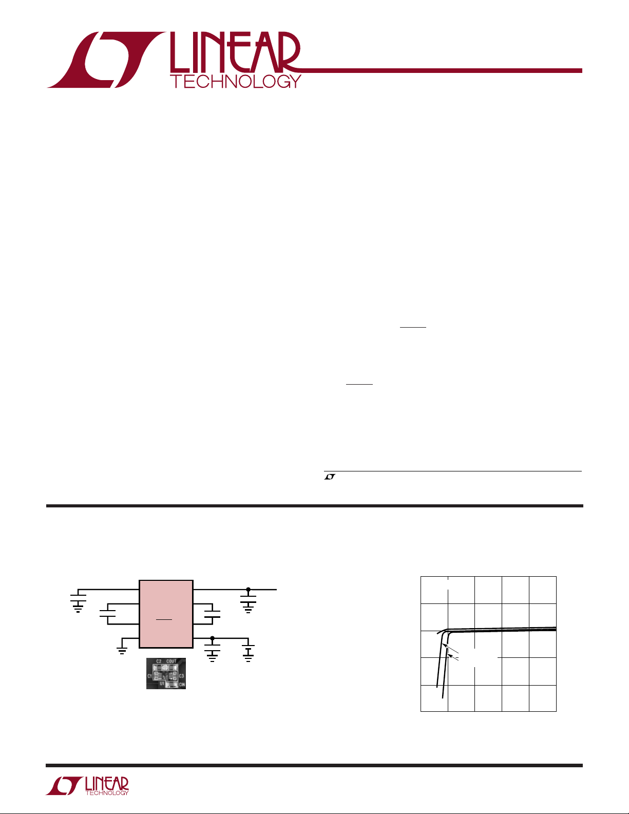
TYPICAL APPLICATIO
Single Cell to 3.3V DC/DC Converter
10µF
1
C2
2
C1
1µF
3
C1–/SHDN
4
GND
PCB LAYOUT FITS IN <0.125IN
V
+
LTC1502-3.3
OUT
C3
C3
+
–
V
IN
U
Output Voltage vs Input Voltage
3.5
8
7
1µF
6
5
10µF
2
V
OUT
I
OUT
10µF
V
IN
SINGLE CELL
NiCd or
ALKALINE
= 3.3V
= 10mA
1502-3.3 TA01
TA = 25°C
3.4
3.3
3.2
OUTPUT VOLTAGE (V)
3.1
3.0
0.8
1.0
I
= 10mA
OUT
= 15mA
I
OUT
1.4
1.2
INPUT VOLTAGE (V)
1.6
1502-3.3 TA02
1.8
1
Page 2
LTC1502-3.3
1
2
3
4
8
7
6
5
TOP VIEW
V
OUT
C3
+
C3
–
V
IN
C2
C1
+
C1–/SHDN
GND
S8 PACKAGE
8-LEAD PLASTIC SO
WW
W
ABSOLUTE MAXIMUM RATINGS
U
(Note 1)
VIN to GND.................................................. –0.3V to 2V
V
to GND ............................................... – 0.3V to 5V
OUT
All Other Pins to GND ................................. –0.3V to 5V
V
Short-Circuit Duration............................ Indefinite
OUT
Storage Temperature Range ................ –65°C to 150°C
U
W
PACKAGE/ORDER INFORMATION
ORDER PART
TOP VIEW
C2
+
C1
C1–/SHDN
GND
8-LEAD PLASTIC MSOP
T
JMAX
1
2
3
4
MS8 PACKAGE
= 125°C, θJA = 250°C/ W
8
V
OUT
+
7
C3
–
6
C3
5
V
IN
Consult factory for Military grade parts.
NUMBER
LTC1502CMS8-3.3
MS8 PART MARKING
LTEC
Operating Temperature Range
Commercial ............................................ 0°C to 70°C
Extended Commercial (Note 4).......... –40°C to 85°C
Industrial ........................................... –40°C to 85°C
Lead Temperature (Soldering, 10 sec)................. 300°C
U
ORDER PART
NUMBER
LTC1502CS8-3.3
LTC1502IS8-3.3
S8 PART MARKING
150233
T
= 125°C, θJA = 150°C/ W
JMAX
502I33
ELECTRICAL CHARACTERISTICS
The ● denotes the specifications which apply over the full operating temperature range, otherwise specifications are at TA = 25°C.
VIN = 0.9V to 1.8V, C1 = C3 = 1µF, CIN = C2 = C
PARAMETER CONDITIONS MIN TYP MAX UNITS
VIN Operating Voltage ● 0.9 1.8 V
Minimum VIN Start-Up Voltage TA = 0°C to 70°C (Note 2) ● 0.75 0.9 V
V
Voltage I
OUT
VIN Operating Current I
VIN Shutdown Current C1–/SHDN = 0V ● 515 µA
Output Ripple I
Efficiency VIN = 1V, I
Switching Frequency Oscillator Free-Running 500 kHz
C1–/SHDN Shutdown Input Threshold C1–/SHDN in Hi-Z Sampling State ● 0.20 0.55 0.85 V
C1–/SHDN Shutdown Input Current C1–/SHDN = 0V (Note 3) ● –0.5 –2.5 – 8 µA
V
Turn-On Time VIN = 1V, I
OUT
V
Short-Circuit Current VIN = 1.5V, V
OUT
Note 1: Absolute Maximum Ratings are those values beyond which the life
of the device may be impaired.
Note 2: Start-up testing is done with a 100kΩ equivalent load on V
Note 3: Currents flowing into the device are positive polarity. Currents
flowing out of the device are negative polarity.
2
= 10µF unless otherwise specified.
OUT
T
= –40°C to 85°C (Note 2) ● 1.1 V
A
≤ 3.5mA, 0.9V ≤ VIN ≤ 1.8V ● 3.17 3.3 3.43 V
OUT
≤ 10mA, 1V ≤ VIN ≤ 1.8V ● 3.17 3.3 3.43 V
I
OUT
= 0mA ● 40 90 µA
OUT
= 10mA, VIN = 1.25V 50 mV
OUT
= 10mA 77 %
OUT
= 0mA 5 ms
OUT
Forced to 0V 20 mA
OUT
Note 4: Commercial grade specifications are guaranteed over the 0°C to
70°C operating temperature range. In addition, commercial grade
OUT
.
specifications are assured over the –40°C to 85°C operating temperature
range by design, characterization and correlation with statistical process
controls. Industrial grade specifications are guaranteed and tested over the
–40°C to 85°C operating temperature range.
P-P
Page 3
UW
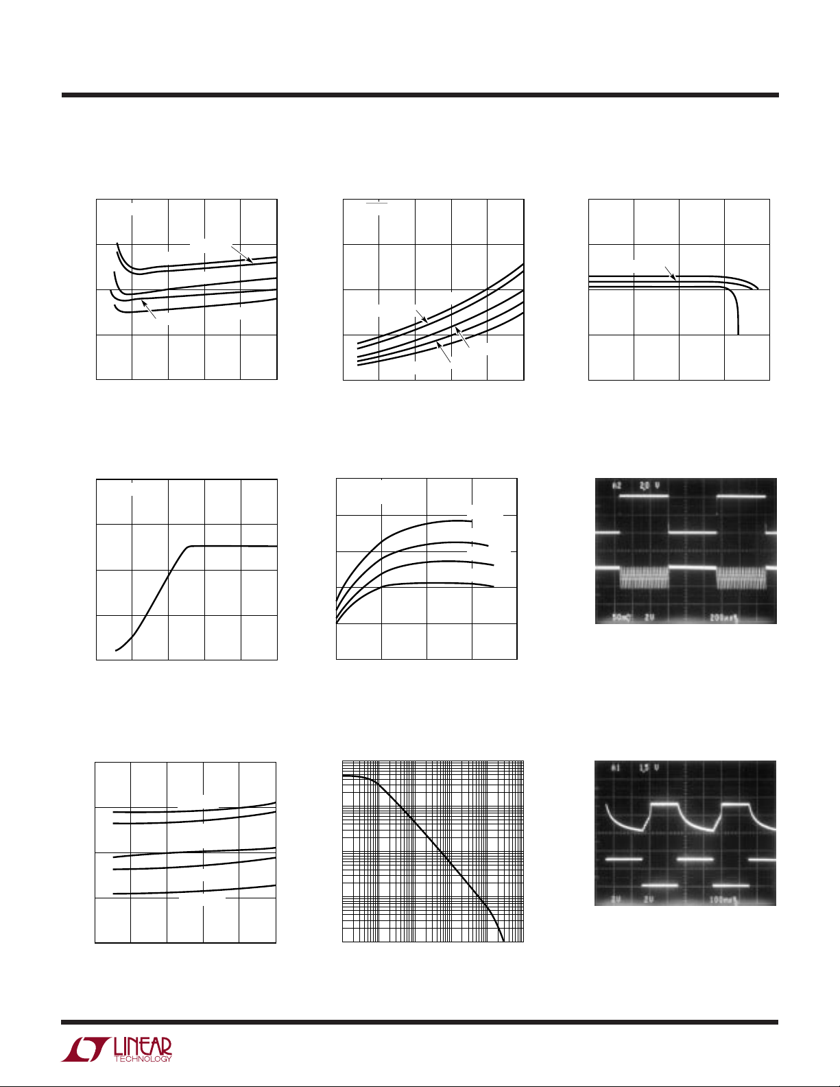
TYPICAL PERFOR A CE CHARACTERISTICS
LTC1502-3.3
No Load Input Current
vs Input Voltage
80
I
= 0mA
OUT
60
40
INPUT CURRENT (µA)
20
0
0.8
TA = 85°C
TA = 0°C
1.0
INPUT VOLTAGE (V)
1.2
= 70°C
T
A
TA = 25°C
T
1.4
Maximum Start-Up Load Current
vs Input Voltage
16
TA = 25°C
12
8
LOAD CURRENT (mA)
4
0
0.8
1.0
INPUT VOLTAGE (V)
1.2
1.4
= –40°C
A
1.6
1.6
1502-3.3 G01
1502-3.3 G04
1.8
1.8
Shutdown Input Current
vs Input Voltage
16
–
/SHDN = 0V
C1
12
8
TA = 70°C
INPUT CURRENT (µA)
4
0
1.0
0.8
T
T
= – 40°C
A
1.2
INPUT VOLTAGE (V)
Efficiency vs Output Current
100
TA = 25°C
= 3.3V
V
OUT
80
60
40
EFFICIENCY (%)
20
0
0.01
0.1
OUTPUT CURRENT (mA)
1
= 85°C
A
1.4
T
A
TA = 25°C
= 0°C
1.6
= 1V
V
IN
VIN = 1.25V
VIN = 1.5V
VIN = 1.8V
10
1502-3.3 G05
1502-3.3 G02
100
1.8
Output Voltage vs Output Current
3.40
3.35
3.30
OUTPUT VOLTAGE (V)
3.25
3.20
0.01
I
OUT
0mA to 10mA
5mA/DIV
V
OUT
AC COUPLED
50mV/DIV
= 25°C
T
A
VIN = 1.5V
V
= 1V
IN
0.1
OUTPUT CURRENT (mA)
= 1.8V
V
IN
1
10
Load Transient Response
VIN = 1.25V
T
= 25°C
A
200µs/DIV
100
1502-3.3 G03
1502-3.3 G06
Oscillator Frequency
vs Input Voltage
700
600
500
400
OSCILLATOR FREQUENCY (kHz)
300
0.8
1.0
TA = 85°C
TA = – 40°C
1.2
INPUT VOLTAGE (V)
TA = 70°C
TA = 25°C
TA = 0°C
1.4
1.6
1502-3.3 G07
1.8
Calculated Battery Life,
Battery = 2400mA • Hr AA Cell
100k
10k
1k
BATTERY LIFE (HOURS)
100
10
0.001
0.1 1 100.01 100
AVERAGE LOAD CURRENT (mA)
1502-3.3 G08
Shutdown Waveforms
(See Figure 1)
V
OUT
2V/DIV
OFF
V
CTRL
ON
V
= 1.25V
IN
R
= 10k
LOAD
= 25°C
T
A
100µs/DIV
1502-3.3 G09
3
Page 4

LTC1502-3.3
UUU
PIN FUNCTIONS
C2 (Pin 1): Charge Pump 1 (CP1) Output. This pin also
serves as the input supply for charge pump 2 (CP2). To
ensure proper start-up, the C2 pin must not be externally
loaded. Bypass the C2 pin with a ≥10µF low ESR capacitor
to ground.
C1+ (Pin 2): Charge Pump 1 Flying Capacitor Positive
Terminal.
C1–/SHDN (Pin 3): Charge Pump 1 Flying Capacitor Negative Terminal and Shutdown Input. Pulling this pin to
ground through a ≈100Ω resistor will put the part into
shutdown mode. With a high resistance pull-down FET,
the series resistor may be eliminated. The external pulldown device must be high impedance for normal operation (see Applications Information). Peak voltage present
on this pin is approximately equal to VIN.
W
BLOCK DIAGRAM
GND (Pin 4): Ground. Connect to a ground plane for best
performance.
VIN (Pin 5): Input Supply Voltage. Bypass VIN with a ≥10µF
low ESR capacitor to ground.
C3– (Pin 6): Charge Pump 2 (CP2) Flying Capacitor
Negative Terminal.
C3+ (Pin 7): Charge Pump 2 Flying Capacitor Positive
Terminal.
V
(Pin 8): 3.3V Regulated Output Voltage. V
OUT
disconnected from VIN during shutdown. Bypass V
OUT
is
OUT
with a ≥10µF low ESR capacitor to ground.
C3
HIZ2
C3C1
–
CP2
+
C3
8
2.1M
V
OUT
C
OUT
–
1.2M
C2
SHUTDOWN
–
C1
/SHDN
32
V
IN
5
C
IN
U2
2.5µA
–
+
+
0.55V
HIZ1
CLK1/CLK2
SHDN OSCEN
TIMING
CONTROL
CP1
+
C1
400k
V
IN
C2
1 6 7
–
+
1M
U3
COMP2COMP3
U4
+
C2
V
OUT
BIAS
CONTROL
INTERNAL
V
CC
COMP1
1.2V
REF
4
GND
1502-3.3 BD
4
Page 5

TEST CIRCUIT
LTC1502-3.3
1
1µF
C2
2
C1
LTC1502-3.3
3
C1–/SHDN
4
GND
+
SWITCH
CLOSED FOR
SHUTDOWN
U
10µF
100Ω
100pF
WUU
APPLICATIONS INFORMATION
Regulator Operation
The LTC1502-3.3 uses a quadrupler charge pump DC/DC
converter to produce a boosted output voltage. The
quadrupler charge pump consists of two voltage doubler
charge pumps (CP1 and CP2 on the Block Diagram)
cascaded in series. CP1 doubles the input voltage VIN and
the CP1 output voltage is stored on external capacitor C2.
The C2 pin also serves as the input for doubler CP2 whose
output is stored on the output capacitor C
doubler is controlled by a two-phase clock which is
generated in the Timing Control circuit. On phase one of
the clock, the flying capacitors C1 and C3 are charged to
their respective input voltages. On phase two each charged
flying capacitor is stacked on top of the input voltage and
discharged through an internal switch onto its respective
output. This sequence of charging and discharging the
CP1 and CP2 flying capacitors continues at the free
running oscillator frequency (500kHz typ) until the output
is in regulation.
Regulation is achieved by comparing the divided down
output voltage to a fixed voltage reference. The charge
pump clocks are disabled when the output voltage is
above the desired regulation point set by COMP1. When
the output has dropped below the lower trip point of
COMP1, the charge pump clocks are turned back on until
V
is boosted back into regulation.
OUT
Enhanced Start-Up
Enhanced start-up capability is provided by the COMP2
circuitry. COMP2 compares the divided down C2 voltage
to the input voltage VIN. The COMP2 output disables the
output charge pump CP2 whenever the divided C2 voltage
OUT
. Each
8
V
OUT
7
+
C3
1µF
6
–
C3
5
V
IN
10µF
10µF
V
IN
I
1502-3.3 TC
OUT
is lower than VIN. The CP2 output is thereby forced into a
high impedance state until the voltage on C2 has been
raised above VIN (the C2 pin should not be loaded for
proper start-up). This allows a higher internal gate drive
voltage to be generated (from the C2 pin) before the output
(V
) is connected to a load. Hysteresis in COMP2 forces
OUT
CP2 to be turned ON and OFF while C
is charging up to
OUT
prevent a lockup condition if C2 droops too low during
start-up. By the time the output nears the regulation point,
the C2 voltage is well above the lower trip point of COMP2
and CP2 will remain enabled. This method of disabling the
output charge pump while an internal boosted gate drive
supply is developed allows the part to start up at low
voltages with a larger output current load than would
otherwise be possible.
Shutdown
Shutdown is implemented using an external pull-down
device on the C1–/SHDN pin. The recommended external
pull-down device is an open-drain FET with resistive current limiting (see Figure 1). The pull-down device must sink
up to 300µA and pull down below 0.2V to ensure proper
shutdown operation, however, the actual series resistance
is not critical. The pull-down device must also go into a HiZ state for the LTC1502-3.3 to become active.
The timing control circuitry forces the CP1 switches into
a high impedance state every 16 clock cycles. The Hi-Z
duration is equal to one clock cycle. At the end of the
Hi-Z time interval, the voltage on the C1–/SHDN pin is
sampled. If the C1–/SHDN pin has been pulled to a logic
low state, the part will go into shutdown mode. When the
pull-down device is disabled, an internal pull-up current
5
Page 6

LTC1502-3.3
U
WUU
APPLICATIONS INFORMATION
1
C2
2
+
C1
LTC1502-3.3
3
C1–/SHDN
4
100Ω
ON OFF
V
CTRL
Figure 1. Pull-Down Circuitry for Shutdown
GND
will force a logic high on the C1–/SHDN pin and put the part
back into active mode. If no external pull-down is present
during the Hi-Z interval, the internal pull-up current will
maintain a logic high on the C1–/SHDN pin thereby keeping the part in active mode.
The shutdown feature can be used to prevent charge pump
switching during noise sensitive intervals. Since the charge
pump oscillator is disabled during shutdown, output switching noise can be eliminated while the external pull-down is
active. The LTC1502-3.3 takes between 20µs and 50µs to
switch from shutdown to active mode once the pull-down
device has been turned off (assuming a 100pF external
capacitance to GND on the C1–/SHDN pin). A 100k pull-up
resistor from VIN to C1–/SHDN will speed up this transition
by a factor of five at the expense of 10µA or so of additional
shutdown current. To maintain regulation, a sufficiently
large output capacitor must be used to prevent excessive
V
droop while the charge pump is in shutdown. Also,
OUT
there must be adequate time for the charge pump to
recharge the output capacitor while the part is active. In
other words, the average load current must be low enough
for the LTC1502-3.3 to maintain a 3.3V output while the
part is active.
Capacitor Selection
For best performance, it is recommended that low ESR
capacitors be used for CIN, C2 and C
and ripple. The CIN, C2 and C
capacitors should be
OUT
either ceramic or tantalum and should be 10µF or greater.
If the input source impedance is very low (<0.5Ω), C
may not be needed. Ceramic capacitors are recommended
for the flying capacitors C1 and C3 with values of 0.47µF
to 2.2µF. Smaller values may be used in low output current
applications (e.g., I
< 1mA).
OUT
8
V
OUT
7
+
C3
6
–
C3
5
V
IN
to reduce noise
OUT
10µF
1502-3.3 F01
IN
Output Ripple
Normal LTC1502-3.3 operation produces voltage ripple
on the V
pin. Output voltage ripple is required for
OUT
regulation. Low frequency ripple exists due to the hysteresis in the sense comparator and propagation
delays in the charge pump enable/disable circuits. High
frequency ripple is also present mainly from the ESR
(equivalent series resistance) in the output capacitor. Typical output ripple (VIN = 1.25V) under maximum load is
50mV peak-to-peak with a low ESR 10µF output capacitor.
The magnitude of the ripple voltage depends on several
factors. High input voltages increase the output ripple
since more charge is delivered to C
per charging cycle.
OUT
Large output current load and/or a small output capacitor
(<10µF) results in higher ripple due to higher output
voltage dV/dt. High ESR capacitors (ESR > 0.5Ω) on the
output pin cause high frequency voltage spikes on V
OUT
with every clock cycle.
There are several ways to reduce the output voltage ripple.
A larger C
the low and high frequency ripple due to the lower C
capacitor (22µF or greater) will reduce both
OUT
OUT
charging and discharging dV/dt and the lower ESR typically found with higher value (larger case size) capacitors.
A low ESR ceramic output capacitor will minimize the high
frequency ripple, but will not reduce the low frequency
ripple unless a high capacitance value is chosen. A reasonable compromise is to use a 10µF to 22µF tantalum
capacitor in parallel with a 1µF to 3.3µF ceramic capacitor
on V
to reduce both the low and high frequency ripple.
OUT
An RC filter may also be used to reduce high frequency
voltage spikes (see Figure 2).
8
V
OUT
+
LTC1502-3.3
V
OUT
LTC1502-3.3
Figure 2. Output Ripple Reduction Techniques
10µF
TANTALUM
8
+ +
2Ω
10µF10µF
1µF
CERAMIC
V
OUT
V
OUT
1502-3.3 F02
6
Page 7

LTC1502-3.3
U
WUU
APPLICATIONS INFORMATION
Short-Circuit Protection
When the output is shorted to ground, the LTC1502-3.3
will continuously charge the C2 capacitor up to approximately 1.4 times VIN, and then discharge C2 into the
shorted output. Since the discharging of C2 into V
OUT
will
bring the C2 voltage below the COMP2 start-up comparator trip voltage, the output charge pump will be forced
Hi-Z while C2 charges up again. Hence, the internal charge
U
PACKAGE DESCRIPTION
0.007
(0.18)
0.021
± 0.006
(0.53 ± 0.015)
* DIMENSION DOES NOT INCLUDE MOLD FLASH, PROTRUSIONS OR GATE BURRS. MOLD FLASH,
PROTRUSIONS OR GATE BURRS SHALL NOT EXCEED 0.006" (0.152mm) PER SIDE
** DIMENSION DOES NOT INCLUDE INTERLEAD FLASH OR PROTRUSIONS.
INTERLEAD FLASH OR PROTRUSIONS SHALL NOT EXCEED 0.006" (0.152mm) PER SIDE
° – 6° TYP
0
Dimensions in inches (millimeters) unless otherwise noted.
MS8 Package
8-Lead Plastic MSOP
(LTC DWG # 05-08-1660)
0.040
± 0.006
(1.02 ± 0.15)
SEATING
PLANE
0.012
(0.30)
0.0256
REF
(0.65)
BSC
pump gate drive voltage is limited to (1.4)(V
IN(MAX)
C2 pin, and no continuous current is supplied to V
) on the
. The
OUT
resulting output short-circuit current is limited to under
20mA (typ) thereby allowing the LTC1502-3.3 to endure
an indefinite output short circuit without damage. When
the short is removed, the part will start up, and operate
normally.
0.118 ± 0.004*
0.034 ± 0.004
(0.86 ± 0.102)
0.006 ± 0.004
(0.15 ± 0.102)
(3.00 ± 0.102)
0.193 ± 0.006
(4.90 ± 0.15)
8
7
12
6
5
0.118 ± 0.004**
4
3
(3.00 ± 0.102)
MSOP (MS8) 1098
0.010 – 0.020
(0.254 – 0.508)
0.008 – 0.010
(0.203 – 0.254)
*
DIMENSION DOES NOT INCLUDE MOLD FLASH. MOLD FLASH
SHALL NOT EXCEED 0.006" (0.152mm) PER SIDE
**
DIMENSION DOES NOT INCLUDE INTERLEAD FLASH. INTERLEAD
FLASH SHALL NOT EXCEED 0.010" (0.254mm) PER SIDE
× 45°
0.016 – 0.050
(0.406 – 1.270)
(1.346 – 1.752)
0°– 8° TYP
Information furnished by Linear Technology Corporation is believed to be accurate and reliable.
However, no responsibility is assumed for its use. Linear Technology Corporation makes no representation that the interconnection of its circuits as described herein will not infringe on existing patent rights.
S8 Package
8-Lead Plastic Small Outline (Narrow 0.150)
(LTC DWG # 05-08-1610)
0.053 – 0.069
0.004 – 0.010
(0.101 – 0.254)
0.014 – 0.019
(0.355 – 0.483)
TYP
0.050
(1.270)
BSC
0.228 – 0.244
(5.791 – 6.197)
0.189 – 0.197*
(4.801 – 5.004)
7
8
1
2
5
6
0.150 – 0.157**
(3.810 – 3.988)
SO8 1298
3
4
7
Page 8

LTC1502-3.3
U
TYPICAL APPLICATIONS
Single Cell to 3.3V DC/DC Converter with Shutdown
SHDN
µCONTROLLER
10µF
100Ω
1µF
1
C2
2
C1
3
C1–/SHDN
4
GND
+
LTC1502-3.3
8
V
OUT
7
+
C3
1µF
6
–
C3
5
V
IN
10µF
V
OUT
I
OUT
10µF
SINGLE CELL
NiCd OR
ALKALINE
= 10mA
1502-3.3 TA03
Single Cell Battery Backup Supply with Autoswitchover and No Reverse Current
MAIN
SUPPLY
5V
TRICKLE
CHARGE
150k
1 CELL
NiCd
10µF
10µF
31
LT1521-3.3
1µF
1µF
1
7
6
5
C2
+
C3
LTC1502-3.3
–
C1–/SHDN
C3
V
IN
2
8
V
OUT
2
+
C1
3
4
GND
1µF
100Ω
= 3.3V
V
= 3.3V
OUT
= 300mA
I
OUT
= 10mA
(I
OUT
IN BACKUP MODE)
10µF
1.1M
470k
*REFERRED TO MAIN SUPPLY
3.9V V
TRIP
*
3
4
5
6
LTC1540
+
–
21
7
8
Q1
2N7002
LOGIC LOW =
BACKUP MODE
1502-3.3 TA04
RELATED PARTS
PART NUMBER DESCRIPTION COMMENTS
LT1307/LT1307B 750mA Single Cell Micropower 600kHz PWM DC/DC Converter 3.3V at 75mA from 1 Cell, MSOP Package
LT1308A/LT1308B 2A Single Cell Micropower 600kHz PWM DC/DC Converter 3.3V at 300mA from 1 Cell, SO-8 Package
LTC1517-3.3 Micropower Regulated 3.3V Charge Pump DC/DC Converter I
LTC1558/LTC1559 Backup Battery Controller with Programmable Output Uses Single NiCd Cell, 100mW Output (Min)
LT1610 Single Cell Micropower 1.7MHz PWM DC/DC Converter 30µA IQ, MSOP Package
LT1611 1.4MHz Inverting Switching Regulator 5V to – 5V at 150mA, Low Output Noise, SOT-23 package
LT1613 1.4MHz Boost Switching Regulator 5V at 200mA from 3.3V Input, SOT-23 Package
LT1615 Micropower Boost Switching Regulator 30µA IQ, V
LTC1682 Low Noise Doubler Charge Pump 60µV
= 15mA (VIN ≥ 2.5V)
OUT
Up to 34V, SOT-23 Package
OUT
Noise, I
RMS
Up to 50mA, MSOP
OUT
8
Linear Technology Corporation
1630 McCarthy Blvd., Milpitas, CA 95035-7417
(408) 432-1900 ● FAX: (408) 434-0507
●
www.linear-tech.com
15023f LT/TP 0899 4K • PRINTED IN USA
LINEAR TECHNOLOGY CORPORATION 1999
 Loading...