

Page 1
FEATURES
LTC1482
Low Power RS485 Transceiver
with Carrier Detect and
Receiver Fail-Safe
U
DESCRIPTIO
■
No Damage or Latchup to ±15kV (Human Body
Model), IEC1000-4-2 Level 4 (±8kV) Contact and
Level 3 (±8kV) Air Discharge
■
Active Low Carrier Detect Output
■
Guaranteed High Receiver Output State for
Floating, Shorted or Terminated Inputs with
No Signal Present
■
Drives Low Cost Residential Telephone Wires
■
Low Power: ICC = 700µA Max with Driver Disabled
■
ICC = 900µA Max in Driver Mode Without Load
■
20µA Max Quiescent Current in Shutdown Mode
■
Single 5V Supply
■
–7V to 12V Common Mode Range Permits ±7V
Ground Difference Between Devices on the Data Line
■
Maximum Data Rate of 4Mbps
■
Power Up/Down Glitch-Free Driver Outputs
■
Up to 32 Transceivers on the Bus
■
Available in 8-Lead MSOP, PDIP and SO Packages
U
APPLICATIO S
■
Battery-Powered RS485/RS422 Applications
■
Low Power RS485/RS422 Transceiver
■
Level Translator
, LTC and LT are registered trademarks of Linear Technology Corporation.
The LTC®1482 is a low power RS485 compatible transceiver that offers an active low carrier detect output. The
open-drain carrier detect pin allows several transceivers
to share the same carrier detect line and can be used to
detect the insertion or removal of a driven RS485/RS422
cable.
Enhanced ESD protection allows the LTC1482 to withstand ±15kV (human body model), IEC-1000-4-2 level 4
(±8kV) contact and level 3 (±8kV) air discharge ESD
without latchup or damage.
The LTC1482 receiver stays alive at all times except in
shutdown. The supply current is a maximum of 700µA
and 900µA when the driver is disabled and enabled
respectively. In shutdown, the quiescent current of the
LTC1482 drops to a maximum of 20µA.
When the driver is disabled or the LTC1482 is in shutdown, the driver outputs are three-stated and remain in
a high impedance state over the RS485 common mode
range.
Excessive power dissipation caused by bus contention or
faults is prevented by a thermal shutdown circuit, which
forces the driver outputs into a high impedance state.
The LTC1482 is fully specified over the commercial and
industrial temperature ranges and is available in 8-lead
MSOP, PDIP and SO packages.
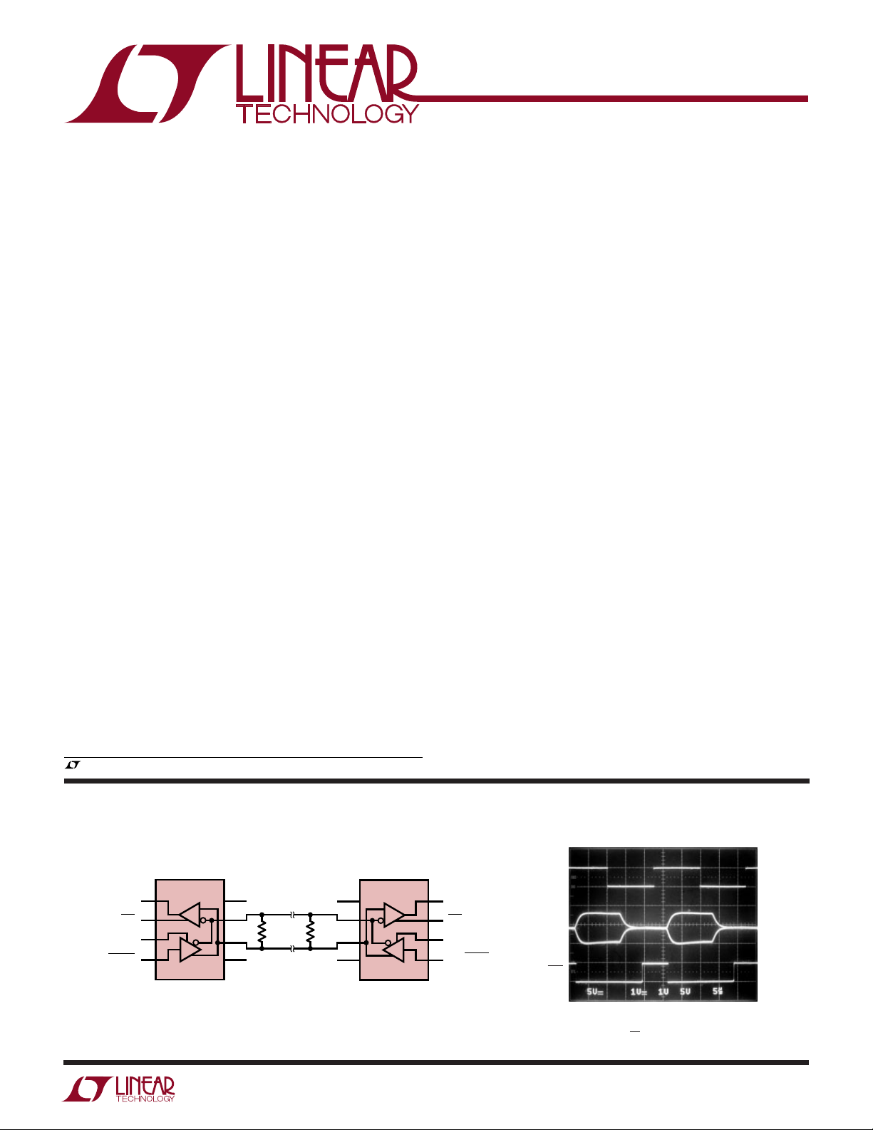
TYPICAL APPLICATIO
RS485 Interface
RO1
CD1
DE1
DI1/SHDN1
LTC1482
R
D
B1
A1
V
CC1
120Ω 120Ω
GND1
U
V
CC2
GND2
Carrier Detect Output (2000 Foot STP Cable)
LTC1482
B2
A2
R
D
RO2
CD2
DE2
DI2/SHDN2
1482 TA01
DE1
A2
B2
CD2
DE1 ↑↓ Dl1 = V
DE2 = 0 Dl2 = V
1k PULL-UP AT CD
CC
CC
1482 TA01a
1
Page 2
LTC1482
WW
W
U
ABSOLUTE MAXIMUM RATINGS
(Note 1)
Supply Voltage (VCC)............................................... 6.5V
Control Input Voltages ................. –0.3V to (VCC + 0.3V)
Carrier Detect Voltage ................................. –0.3V to 8V
Driver Input Voltage ..................... –0.3V to (VCC + 0.3V)
Driver Output Voltages ................................. –7V to 10V
Receiver Input Voltages (Driver Disabled) .. –12V to 14V
Receiver Output Voltage ............... – 0.3V to (VCC + 0.3V)
U
W
U
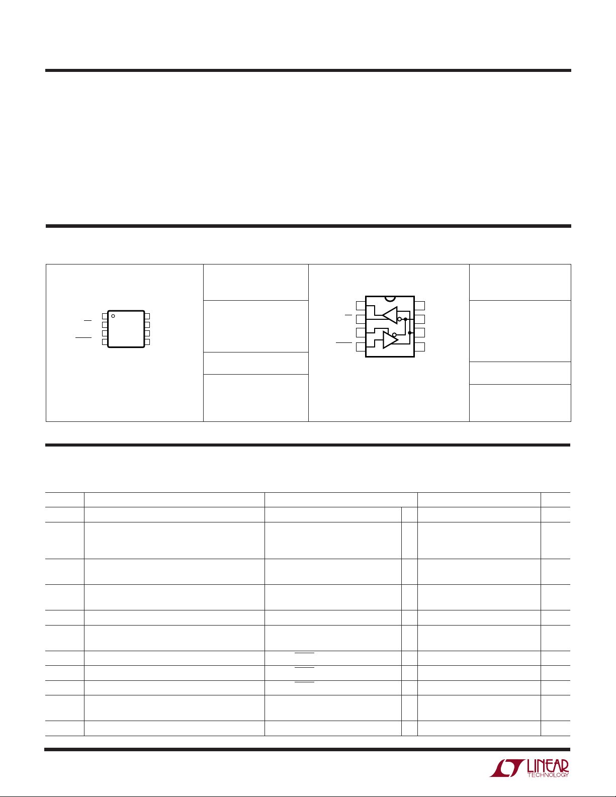
PACKAGE/ORDER INFORMATION
ORDER PART
NUMBER
RO
1
CD
2
DE
3
DI/SHDN
4
8-LEAD PLASTIC MSOP
T
= 125°C, θJA = 200°C/ W
JMAX
TOP VIEW
MS8 PACKAGE
8
V
CC
7
B
6
A
5
GND
LTC1482CMS8 LTC1482CN8
MS8 PART MARKING
LTCB
Junction Temperature .......................................... 125°C
Operating Temperature Range
LTC1482C ........................................ 0°C ≤ TA ≤ 70°C
LTC1482I...................................... –40°C ≤ TA ≤ 85°C
Storage Temperature Range .................. –65°C to 150°C
Lead Temperature (Soldering, 10 sec)...................300°C
ORDER PART
RO
1
CD
2
DE
3
DI/SHDN
4
N8 PACKAGE
8-LEAD PDIP
T
= 125°C, θJA = 130°C/ W (N8)
JMAX
T
= 125°C, θJA = 135°C/W (S8)
JMAX
TOP VIEW
8-LEAD PLASTIC SO
V
8
CC
B
7
A
6
GND
5
S8 PACKAGE
NUMBER
LTC1482CS8
LTC1482IN8
LTC1482IS8
S8 PART MARKING
1482
1482I
Consult factory for Military grade parts.
ELECTRICAL CHARACTERISTICS
temperature range, otherwise specifications are at T
SYMBOL PARAMETER CONDITIONS MIN TYP MAX UNITS
V
OD1
V
OD2
V
OD3
∆V
OD
V
OC
∆|VOC| Change in Magnitude of Driver Common Mode R = 22Ω, 27Ω or R = 50Ω, Figure 1 ● 0.2 V
V
IH
V
IL
I
IN1
I
IN2
V
THRO
Differential Driver Output Voltage (Unloaded) I
Differential Driver Output Voltage (with Load) R = 50Ω (RS422) ● 2V
Differential Driver Output Voltage V
(with Common Mode)
Change in Magnitude of Driver Differential R = 22Ω, 27Ω or R = 50Ω, Figure 1 ● 0.2 V
Output Voltage for Complementary Output States V
Driver Common Mode Output Voltage R = 22Ω, 27Ω or R = 50Ω, Figure 1 ● 3V
Output Voltage for Complementary Output States
Input High Voltage DE, DI/SHDN ● 2V
Input Low Voltage DE, DI/SHDN ● 0.8 V
Input Current DE, DI/SHDN ● ±2 µA
Input Current (A, B) with Driver Disabled DE = 0, VCC = 0 or 5V, VIN = 12V ● 1.0 mA
Differential Input Threshold Voltage for Receiver –7V ≤ VCM ≤ 12V, DE = 0 ● –0.20 –0.015 V
The ● denotes the specifications which apply over the full operating
= 25°C. VCC = 5V ±5% (Notes 2 and 3) unless otherwise noted.
A
= 0 ● V
OUT
R = 27Ω (RS485) Figure 1
R = 22Ω, Figure 1
= –7V to 12V, Figure 2 ● 1.5 5 V
TST
= –7V to 12V, Figure 2
TST
DE = 0, V
= 0 or 5V, VIN = –7V ● –0.8 mA
CC
● 1.5 5 V
● 1.5 5 V
CC
V
2
Page 3
LTC1482
ELECTRICAL CHARACTERISTICS
temperature range, otherwise specifications are at T
The ● denotes the specifications which apply over the full operating
= 25°C. VCC = 5V ±5% (Notes 2 and 3) unless otherwise noted.
A
SYMBOL PARAMETER CONDITIONS MIN TYP MAX UNITS
V
∆V
V
V
I
OZR
THCD
TH
OH
OL
Differential Input Threshold Voltage for CD = 1 –7V ≤ VCM ≤ 12V, DE = 0 ● –0.20 0.20 V
Receiver Input Hysteresis VCM = 0V, DE = 0 ±30 mV
CD Output High Voltage I
RO Output High Voltage I
RO and CD Output Low Voltage I
Three-State (High Impedance) Receiver Output VCC = Max, 0.4V ≤ V
= –10µA, (VA – VB) = 0V ● 3.4 V
OUT
= –4mA, (VA – VB) = 200mV ● 3.5 V
OUT
= 4mA, (VA – VB) = –200mV ● 0.4 V
OUT
≤ 2.4V ● ±1 µA
OUT
Current in Shutdown DI/SHDN = 0, DE = 0
R
IN
I
CC
I
SHDN
I
OSD1
I
OSD2
I
OS
I
PULL-UP
Receiver Input Resistance –7V ≤ VCM ≤ 12V ● 12 22 kΩ
Supply Current No Load, Driver Enabled (DE = VCC) ● 580 900 µA
No Load, Driver Disabled (DE = 0)
● 430 700 µA
Supply Current in Shutdown Mode DE = 0, DI = 0 ● 10 20 µA
Driver Short-Circuit Current, V
Driver Short-Circuit Current, V
RO and CD Short-Circuit Current 0V ≤ V
= High (Note 4) –7V ≤ V
OUT
= Low (Note 4) –7V ≤ V
OUT
≤ 10V 35 250 mA
OUT
≤ 10V 35 250 mA
OUT
OUT
≤ V
CC
● 785mA
CD Pull-Up Current CD = 0V ● 15 30 60 µA
U
SWITCHING CHARACTERISTICS
temperature range, otherwise specifications are at T
The ● denotes the specifications which apply over the full operating
= 25°C. VCC = 5V ±5% (Notes 2 and 3) unless otherwise noted.
A
SYMBOL PARAMETER CONDITIONS MIN TYP MAX UNITS
t
PLH
t
PHL
t
SKEW
tr, t
f
t
ZH
t
ZL
t
LZ
t
HZ
t
ZH(SHDN)
Driver Input to Output R
= 54Ω, CL1 = CL2 = 100pF ● 10 28 60 ns
DIFF
Driver Input to Output (Figures 4, 6) ● 10 30 60 ns
Driver Output to Output ● 210 ns
Driver Rise or Fall Time ● 31540 ns
Driver Enable to Output High CL = 100pF (Figures 5, 7) S2 Closed ● 40 70 ns
Driver Enable to Output Low CL = 100pF (Figures 5, 7) S1 Closed ● 40 100 ns
Driver Disable Time from Low CL = 15pF (Figures 5, 7) S1 Closed ● 40 70 ns
Driver Disable Time from High CL = 15pF (Figures 5, 7) S2 Closed ● 40 70 ns
Driver Enable from Shutdown to Output High CL = 100pF (Figures 5, 7) S2 Closed ● 40 100 ns
(Note 5)
t
ZL(SHDN)
t
HZ(SHDN)
t
LZ(SHDN)
f
MAX
t
PLH
Driver Enable from Shutdown to Output Low CL = 100pF (Figures 5, 7) S1 Closed ● 40 100 ns
Driver Disable on Shutdown from Output High CL = 15pF (Figures 5, 7) S2 Closed ● 40 100 ns
Driver Disable on Shutdown from Output Low CL = 15pF (Figures 5, 7) S1 Closed ● 40 100 ns
Maximum Data Rate (Note 6) ● 4 5 Mbps
Receiver Input to Output (Note 7) R
= 54Ω, CL1 = CL2 = 100pF, ● 30 138 200 ns
DIFF
(Figures 4, 8)
t
PHL
Receiver Input to Output R
= 54Ω, CL1 = CL2 = 100pF, ● 30 122 200 ns
DIFF
(Figures 4, 8)
t
SKD
|t
– t
PLH
| Differential Receiver Skew R
PHL
= 54Ω, CL1 = CL2 = 100pF, 16 ns
DIFF
(Figures 4, 8)
t
t
CDH
CDL
Receiver Input to CD Output High (Note 7) R
Receiver Input to CD Output Low (Note 7) R
= 54Ω, CL1 = CL2 = 100pF, ● 2900 5000 ns
DIFF
(Figures 4, 10) DI/SHDN = V
= 54Ω, CL1 = CL2 = 100pF, ● 150 300 ns
DIFF
(Figures 4, 10) DI/SHDN = V
CC
CC
3
Page 4

LTC1482
U
SWITCHING CHARACTERISTICS
temperature range, otherwise specifications are at T
SYMBOL PARAMETER CONDITIONS MIN TYP MAX UNITS
t
CDH(SHDN)
t
CDL(SHDN)
t
ZH(SHDN)
t
ZL(SHDN)
t
HZ(SHDN)
t
LZ(SHDN)
Receiver Input to CD Output High at Shutdown R
Receiver Input to CD Output Low from Shutdown R
Receiver Enable from Shutdown to Output High CL = 15pF (Figures 3, 9) S2 Closed, ● 30 600 ns
Receiver Enable from Shutdown to Output Low CL = 15pF (Figures 3, 9) S1 Closed, ● 2600 5000 ns
Receiver Disable from High on Shutdown CL = 15pF (Figures 3, 9) S2 Closed, ● 200 600 ns
Receiver Disable from Low on Shutdown CL = 15pF (Figures 3, 9) S1 Closed, ● 200 600 ns
The ● denotes the specifications which apply over the full operating
= 25°C. VCC = 5V ±5% (Notes 2 and 3) unless otherwise noted.
A
= 54Ω, CL1 = CL2 = 100pF, ● 2600 5000 ns
DIFF
(Figures 4, 11) DI/SHDN = DE
= 54Ω, CL1 = CL2 = 100pF, ● 2600 5000 ns
DIFF
(Figures 4, 11) DI/SHDN = DE
A = 750mV, B = –750mV, DE = 0,
DI/SHDN =
A = –750mV, B = 750mV, DE = 0,
DI/SHDN =
A = 750mV, B = –750mV, DE = 0,
DI/SHDN =
A = –750mV, B = 750mV, DE = 0,
DI/SHDN =
Note 1: Absolute Maximum Ratings are those values beyond which the life of
a device may be impaired.
Note 2: All typicals are given for V
= 5V and TA = 25°C.
CC
Note 3: All currents into device pins are positive; all currents out of device
pins are negative. All voltages are referenced to device ground unless
otherwise specified.
Note 4: For higher ambient temperatures, the part may enter thermal
shutdown during short-circuit conditions.
Note 5: Both driver input and driver enable pins are pulled high
simultaneously.
Note 6: Guaranteed by design.
Note 7: Measured with an external LTC1485 driver.
UW
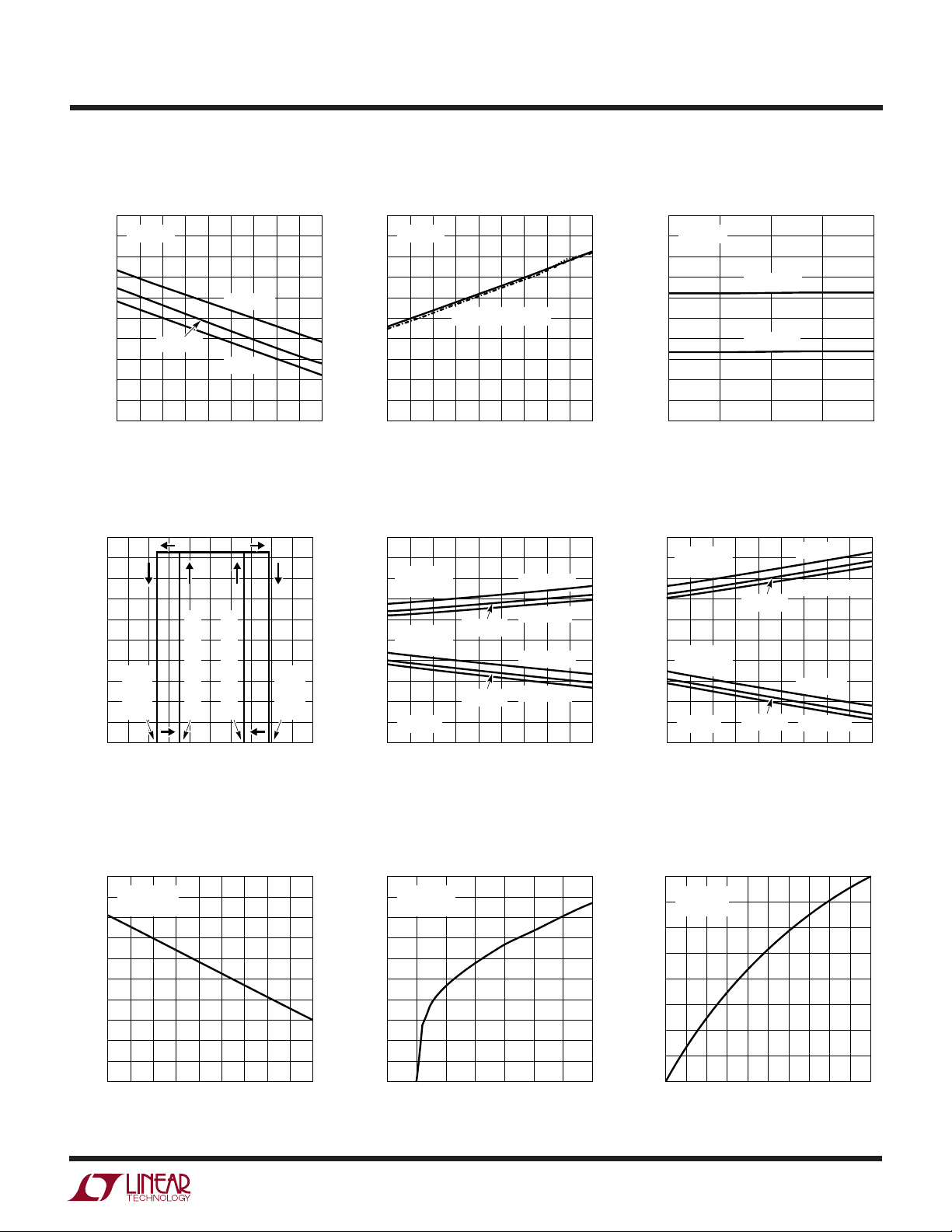
TYPICAL PERFOR A CE CHARACTERISTICS
Receiver Output Voltage vs Input
Voltage
6
TA = 25°C
5
4
3
2
1
RECEIVER OUTPUT VOLTAGE (V)
V
THRO(LOW)
0
–0.16 –0.12 –0.08 –0.04 0
–0.2
INPUT VOLTAGE (V)
V
THRO(HIGH)
1482 G01
Receiver Input Threshold Voltage
(Output High) vs Temperature
0
–0.02
–0.04
–0.06
–0.08
–0.1
–0.12
–0.14
–0.16
–0.18
RECEIVER INPUT THRESHOLD VOLTAGE (mV)
–0.20
–55 –35 –15 5 25 45 65 85 105 125
VCM = 12V
VCM = 0V
TEMPERATURE (°C)
VCC = 5V
V
VCM = –7V
THRO(HIGH)
1482 G02
Receiver Input Threshold Voltage
(Output Low) vs Temperature
0
–0.02
–0.04
–0.06
–0.08
–0.1
–0.12
–0.14
–0.16
–0.18
RECEIVER INPUT THRESHOLD VOLTAGE (mV)
–0.20
–55 –35 –15 5 25 45 65 85 105 125
VCM = 12V
VCM = 0V
TEMPERATURE (°C)
VCC = 5V
V
VCM = –7V
THRO(LOW)
1482 G03
4
Page 5
UW
TEMPERATURE (°C)
CARRIER DETECT THRESHOLD VOLTAGE (V)
1482 G09
0.25
0.20
0.15
0.10
0.05
0
–0.05
–0.10
–0.15
–0.20
–0.25
VCC = 5V
POSITIVE
V
THCD(LOW)
NEGATIVE
V
THCD(LOW)
–55 –35 –15 5 25 45 65 85 105 125
VCM = 12V
VCM = –7V
VCM = 12V
VCM = –7V
VCM = 0V
VCM = 0V
TYPICAL PERFOR A CE CHARACTERISTICS
LTC1482
Receiver Input Offset Voltage vs
Temperature
0
VCC = 5V
–20
–40
–60
–80
–100
–120
–140
–160
–180
RECEIVER INPUT OFFSET VOLTAGE (mV)
–200
–55 –35 –15 5 25 45 65 85 105 125
VCM = 0V
TEMPERATURE (°C)
VCM = 12V
VCM = –7V
Carrier Detect Output Voltage vs
Receiver Input Voltage
5.0
4.5
4.0
3.5
3.0
2.5
2.0
1.5
1.0
0.5
CARRIER DETECT OUTPUT VOLTAGE (V)
0
–0.25
THCD(LOW)
NEGATIVE
V
–0.15 –0.05 0.05 0.15 0.25
RECEIVER INPUT VOLTAGE (V)
THCD(HIGH)
THCD(HIGH)
NEGATIVE, V
POSITIVE, V
1482 G04
THCD(LOW)
POSITIVE
V
1482 G07
Receiver Hysteresis vs
Temperature
100
VCC = 5V
90
80
70
60
50
40
HYSTERESIS (mV)
30
20
10
0
–55 –35 –15 5 25 45 65 85 105 125
VCM = –7V TO 12V
TEMPERATURE (°C)
Carrier Detect Threshold Voltage
(Output High) vs Temperature
0.25
0.20
POSITIVE
0.15
V
THCD(HIGH)
0.10
0.05
NEGATIVE
0
V
–0.05
–0.10
–0.15
–0.20
CARRIER DETECT THRESHOLD VOLTAGE (V)
–0.25
THCD(HIGH)
VCC = 5V
–55 –35 –15 5 25 45 65 85 105 125
VCM = 0V
VCM = 0V
TEMPERATURE (°C)
VCM = 12V
VCM = –7V
VCM = 12V
VCM = –7V
1482 G05
1482 G08
Receiver Input Threshold Voltage
vs Supply Voltage
0
TA = 25°C
–0.02
–0.04
–0.06
–0.08
–0.10
–0.12
–0.14
–0.16
–0.18
RECEIVER INPUT THRESHOLD VOLTAGE (V)
–0.20
4.5
V
THRO(HIGH)
V
THRO(LOW)
4.75 5 5.25 5.5
SUPPLY VOLTAGE (V)
Carrier Detect Threshold Voltage
(Output Low) vs Temperature
1482 G06
Receiver Output High Voltage vs
Temperature
4.5
VCC = 4.75V
4.4
4.3
4.2
4.1
4.0
3.9
3.8
3.7
RECEIVER OUTPUT HIGH VOLTAGE (V)
3.6
3.5
= –8mA
I
OUT
–55 –35 –15 5 25 45 65 85 105 125
TEMPERATURE (°C)
1482 G10
Carrier Detect Output High
Voltage vs Output Current
5.0
VCC = 4.75V
4.5
= 25°C
T
A
4.0
3.5
3.0
2.5
2.0
1.5
1.0
0.5
CARRIER DETECT OUTPUT HIGH VOLTAGE (V)
0
–35 –30 –25 –20 –15 –10 –5 0
OUTPUT CURRENT (µA)
1482 G11
Receiver and Carrier Detect
Output Low Voltage vs Output
Current
40
TA = 25°C
35
= 4.75
V
CC
30
25
20
15
OUTPUT CURRENT (mA)
10
5
0
0
0.2 0.4 0.6 0.8 1 1.2 1.4 1.6 1.8 2
OUTPUT LOW VOLTAGE (V)
1482 G12
5
Page 6

LTC1482
UW
TYPICAL PERFOR A CE CHARACTERISTICS
Receiver Output High Voltage vs
Temperature
4.8
VCC = 4.75V
4.6
I = 8mA
4.4
4.2
4.0
3.8
3.6
OUTPUT VOLTAGE (V)
3.4
3.2
3.0
–55 –35 –15 5 25 45 65 85 105 125
TEMPERATURE (°C)
1482 G13
Carrier Detect Output High
Voltage vs Temperature
4.00
VCC = 4.75V
3.95
3.90
3.85
3.80
3.75
3.70
3.65
3.60
3.55
CARRIER DETECT OUTPUT HIGH VOLTAGE (V)
3.50
= 10µA
I
OUT
V
OH
–55 –35 –15 5 25 45 65 85 105 125
TEMPERATURE (°C)
1482 G14
Receiver and Carrier Detect
Output Low Voltage vs
Temperature
0.50
VCC = 4.75V
0.45
0.40
0.35
0.30
0.25
0.20
0.15
RECEIVER AND CARRIER
0.10
DETECT OUTPUT LOW VOLTAGE
0.05
= 8mA
I
OUT
0
–55 –35 –15 5 25 45 65 85 105 125
TEMPERATURE (°C)
1482 G15
Receiver Propagation Delay vs
Temperature Receiver Skew vs Temperature
200
VCC = 5V
180
160
140
120
100
80
60
40
RECEIVER PROPAGATION DELAY (ns)
20
0
–55 –35 –15 5 25 45 65 85 105 125
t
PLH
t
PHL
TEMPERATURE (°C)
1482 G16
30
VCC = 5V
25
20
15
10
RECEIVER SKEW (ns)
5
0
–55 –35 –15 5 25 45 65 85 105 125
|t
– t
PLH
PHL
TEMPERATURE (°C)
Receiver Short-Circuit Current vs
Temperature Supply Current vs Temperature
100
VCC = 5.25V
90
80
70
60
50
40
30
20
10
RECEIVER SHORT-CIRCUIT CURRENT (mA)
0
–55 –35 –15 5 25 45 65 85 105 125
OUTPUT LOW
SHORT TO V
OUTPUT HIGH
SHORT TO GROUND
TEMPERATURE (°C)
CC
1482 G19
1000
VCC = 5V
900
800
700
600
500
400
300
SUPPLY CURRENT (µA)
200
100
DRIVER ENABLED
NO LOAD
DRIVER DISABLED
0
–30 –5 20 45 70 95 120 145 170
–55
THERMAL SHUTDOWN
WITH DRIVER
ENABLED
TEMPERATURE (°C)
Receiver Propagation Delay vs
Supply Voltage
150
TA = 25°C
t
140
|
1482 G17
130
120
110
RECEIVER PROPAGATION DELAY (ns)
100
4.5
4.75 5 5.25 5.5
PLH
t
PHL
SUPPLY VOLTAGE (V)
1482 G18
Logic Input Threshold vs
Temperature
2.00
1.95
1.90
1.85
1482 G20
1.80
1.75
1.70
1.65
1.60
1.55
LOGIC INPUT THRESHOLD VOLTAGE (V)
1.50
–55
VCC = 5.25V
VCC = 4.75V
–35 –15 5 25 45 65 85 105 125
TEMPERATURE (°C)
VCC = 5V
1482 G21
6
Page 7

UW
OUTPUT CURRENT (mA)
0
10 20 30 40 50 60 70 80 90 100
DRIVER DIFFERENTIAL OUTPUT VOLTAGE (V)
1482 G30
5.0
4.5
4.0
3.5
3.0
2.5
2.0
1.5
1.0
0.5
0
VCC = 5V
TYPICAL PERFOR A CE CHARACTERISTICS
LTC1482
Driver Differential Output Voltage
vs Temperature
3.0
2.5
2.0
VCC = 5.25V
1.5
1.0
0.5
0
DRIVER DIFFERENTIAL OUTPUT VOLTAGE (V)
–0.5
–55
–35 –15 5 25 45 65 85 105 125
VCC = 5V
VCC = 4.75V
∆VOD, VCC = 4.5V TO 5.25V
TEMPERATURE (°C)
RL = 44Ω
VCC = 4.5V
Driver Common Mode Output
Voltage vs Temperature
3.0
2.5
2.0
1.5
VCC = 5.25V
VCC = 5V
RL = 44Ω
VCC = 4.75V
VCC = 4.5V
1482 G22
Driver Differential Output Voltage
vs Temperature
3.0
2.5
VCC = 5.25V
2.0
1.5
1.0
0.5
0
DRIVER DIFFERENTIAL OUTPUT VOLTAGE (V)
–0.5
–55
–35 –15 5 25 45 65 85 105 125
VCC = 5V
VCC = 4.75V
∆VOD, VCC = 4.5V TO 5.25V
TEMPERATURE (°C)
RL = 54Ω
VCC = 4.5V
Driver Common Mode Output
Voltage vs Temperature
3.0
2.5
2.0
1.5
VCC = 5.25V
VCC = 5V
RL = 54Ω
VCC = 4.75V
VCC = 4.5V
1482 G23
Driver Differential Output Voltage
vs Temperature
3.5
3.0
2.5
VCC = 5.25V
2.0
1.5
1.0
0.5
0
DRIVER DIFFERENTIAL OUTPUT VOLTAGE (V)
–0.5
–35 –15 5 25 45 65 85 105 125
–55
VCC = 5V
∆VOD, VCC = 4.5V TO 5.25V
TEMPERATURE (°C)
RL = 100Ω
VCC = 4.75V
VCC = 4.5V
Driver Common Mode Output
Voltage vs Temperature
3.0
2.5
2.0
1.5
VCC = 5.25V
VCC = 5V
RL = 100Ω
VCC = 4.75V
VCC = 4.5V
1482 G24
1.0
0.5
DRIVER COMMON MODE VOLTAGE (V)
0
–55
∆VOC, VCC = 4.5V TO 5.25V
–35 –15 5 25 45 65 85 105 125
TEMPERATURE (°C)
Driver Differential Output Voltage
vs Temperature
3.5
SEE FIGURE 2
3.0
2.5
VCC = 5.25V
2.0
1.5
1.0
0.5
0
DRIVER DIFFERENTIAL OUTPUT VOLTAGE (V)
–0.5
–35 –15 5 25 45 65 85 105 125
–55
VCC = 5V
∆V
FOR VCC = 4.5V TO 5.25V
OD3
TEMPERATURE (°C)
VCC = 4.75V
1482 G25
VCM = –7V
V
OD3
DI/SD HIGH
VCC = 4.5V
1482 G28
1.0
0.5
DRIVER COMMON MODE VOLTAGE (V)
0
–55
∆VOC, VCC = 4.5V TO 5.25V
–35 –15 5 25 45 65 85 105 125
TEMPERATURE (°C)
Driver Differential Output Voltage
vs Temperature
3.0
2.5
2.0
VCC = 5.25V
1.5
VCM = 12V
V
OD3
1.0
DI/SD HIGH
SEE FIGURE 2
0.5
0
DRIVER DIFFERENTIAL OUTPUT VOLTAGE (V)
–0.5
–35 –15 5 25 45 65 85 105 125
–55
VCC = 5V
∆V
FOR VCC = 4.5V TO 5.25V
OD3
TEMPERATURE (°C)
VCC = 4.75V
VCC = 4.5V
1482 G26
1482 G29
1.0
0.5
DRIVER COMMON MODE VOLTAGE (V)
0
–55
∆VOC, VCC = 4.5V TO 5.25V
–35 –15 5 25 45 65 85 105 125
TEMPERATURE (°C)
Driver Differential Output Voltage
vs Output Current
1482 G27
7
Page 8

LTC1482
UW
TYPICAL PERFOR A CE CHARACTERISTICS
Driver Output High Voltage vs
Output Current
5.0
VCC = 4.75V
4.5
4.0
3.5
3.0
2.5
2.0
1.5
1.0
DRIVER OUTPUT HIGH VOLTAGE (V)
0.5
0
–90 –80 –70 –60 –50 –40 –30 –20 –10 0
–100
OUTPUT CURRENT (mA)
Driver Skew vs Temperature
5.0
4.5
4.0
3.5
3.0
2.5
2.0
DRIVER SKEW (ns)
1.5
1.0
0.5
0
–35 –15 5 25 45 65 85 105 125
–55
TEMPERATURE (°C)
1482 G31
1482 G34
Driver Output Low Voltage vs
Output Current
3.0
VCC = 4.75V
2.5
2.0
1.5
1.0
0.5
DRIVER OUTPUT LOW VOLTAGE (V)
0
10 20 30 40 50 60 70 80 90 100
0
OUTPUT CURRENT (mA)
Driver Propagation Delay vs
Supply Voltage
40
TA = 25°C
35
30
25
20
15
10
DRIVER PROPAGATION DELAY (ns)
5
0
4.5
4.75 5 5.25 5.5
t
PHL
t
PLH
SUPPLY VOLTAGE (V)
1482 G32
1482 G35
Driver Propagation Delay vs
Temperature
40
VCC = 5V
35
30
25
20
15
10
DRIVER PROPAGATION DELAY (ns)
5
0
–35 –15 5 25 45 65 85 105 125
–55
t
PLH
t
PHL
TEMPERATURE (°C)
Driver Short-Circuit Current vs
Temperature
250
200
150
100
50
DRIVER SHORT-CIRCUIT CURRENT (mA)
0
–55
DRIVER OUTPUT HIGH
SHORT TO –7V
DRIVER OUTPUT LOW
SHORT TO 10V
–35 –15 5 25 45 65 85 105 125
TEMPERATURE (°C)
VCC = 5.25V
1482 G33
1482 G36
UUU
PIN FUNCTIONS
RO (Pin 1): Receiver Output. If a carrier is present (CD low)
and the part is not in shutdown, RO is high if the receiver
input differential voltage (A – B) ≥ V
(A – B) ≤ V
THRO(MIN)
. RO is forced to high (fail-safe state)
THRO(MAX)
and low if
if a carrier is not present (CD = 1). In shutdown, RO is
three-stated. If the driver is enabled, RO follows the logic
level at the driver input.
CD (Pin 2): Open-Drain Carrier Detect Output. Provided
that the part is not in shutdown, the CD output is low if
V
THCD(MIN)
< (A – B) < V
≥ (A – B) ≥ V
THCD(MAX)
. This is true regardless of whether
THCD(MAX)
and high if V
THCD(MIN)
the A and B pins are driven by the internal (DE = 1) or an
8
external (DE = 0) driver. A weak internal pull-up removes
the need for an external pull-up resistor if fast rise times
are not important. Several LTC1482s can share the same
CD line. CD = 1 forces RO to the high fail-safe state. In
shutdown, CD is three-stated. This pin can be pulled above
VCC but should not be taken above 8V to avoid damage.
DE (Pin 3): Driver Enable Input. DE = 0 disables or threestates the driver outputs. DE = 1 enables the driver outputs
with the high/low state of the outputs set by DI/SHDN.
DI/SHDN (Pin 4): Driver Input and Shutdown Input. It is
used together with the DE pin to put the part in shutdown
Page 9

UUU
PIN FUNCTIONS
LTC1482
(DE = 0, DI/SHDN = 0) or to disable the driver while keeping
the receiver alive (DE = 0, DI/SHDN = 1). When the driver
is enabled (DE = 1), DI/SHDN = 0 forces the A output low
and the B output high. DI/SHDN = 1 forces the A output
high and the B output low.
GND (Pin 5): Ground.
A (Pin 6): Driver Output/Receiver Input. The input resis-
tance is typically 22k when the driver is disabled (DE = 0).
U
U
FU CTIO TABLES
Driver Enabled (DE = 1)
DI/SHDN A B RO CD
00100
11010
X A Shorted to B 1 1
Note 1: DE = 0, DI/SHDN = 0 puts the part in ICC shutdown and the supply
current drawn by the V
alive except in shutdown.
Note 2: The table is valid regardless of the presence of an external
termination resistor.
Note 3: Although the RO and the driver outputs are three-stated, the A and
B pins each present a 22kΩ receiver input resistance to ground.
pin drops to 20µA max. The receiver is always
CC
When the driver is enabled, the A output follows the logic
level at the DI/SHDN pin.
B (Pin 7): Driver Output/Receiver Input. The input resistance is typically 22k when the driver is disabled (DE = 0).
When the driver is enabled, the B output is inverted from
the logic level at the DI/SHDN pin.
VCC (Pin 8): Positive Supply. 4.75V < V
< 5.25V. A 0.1µF
CC
bypass capacitor is recommended.
Driver Disabled (DE = 0, Notes 1, 2)
DI/SHDN A – B RO CD
0 X (Note 3) Z 1 (Internal Pull-Up)
1V
THCD(MIN)
1 A and B are Open 1 1
1 A and B are Shorted 1 1
1V
1V
THCD(MIN)
THCD(MIN)
X = Don’t Care
Z = High Impedance
< (A – B) < V
≥ (A – B) ≥ V
and (A – B) ≤ V
≥ (A – B) ≥ V
and (A – B) ≥ V
THCD(MAX)
THCD(MAX)
THRO(MIN)
THCD(MAX)
THRO(MAX)
11
00
10
TEST CIRCUITS
15pF
60Ω
375Ω
375Ω
V
CC
1k
1482 F04
CD
RO
1482 F02
V
TST
–7V TO 12V
RECEIVER
OUTPUT
OUTPUT
UNDER TEST
TEST POINT
C
500Ω
C
L
L
Figure 5. Driver Timing Test Load
S1
1k
S2
S1
S2
1482 F05
1k
V
CC
A
R
V
OD
V
OC
R
B
1482 F01
Figure 1. Driver DC Test Load #1 Figure 3. Receiver Timing Test Load
DE
A
DI
R
DIFF
B
C
L1
C
L2
A
V
OD3
B
Figure 2. Driver DC Test Load #2
A
B
Figure 4. Driver/Receiver Timing Test Load
1482 F03
V
CC
9
Page 10

LTC1482
UWW
SWITCHI G TI E WAVEFOR S
DI/SHDN
A, B
A, B
3V
0V
V
O
–V
O
B
A
3V
DE
0V
5V
V
V
OH
0V
V
O
1/2 V
NOTE: DE = 1
OL
NOTE: DI = 0 FOR t
1.5V
t
PLH
t
DSKEW
90%
10%
t
r
O
50%
t
SKEW
f = 1MHz, tr ≤ 10ns, tf ≤ 10ns
VO = V(A) – V(B)
1.5V
t
PHL
90%
50%
10%
t
f
SKEW
1482 F06
t
Figure 6. Driver Propagation Delays
1.5V
ZL(SHDN)
t
ZL(SHDN), tZL
2.3V
2.3V
t
ZH(SHDN), tZH
, t
LZ(SHDN)
; DI = DE FOR t
f = 1MHz, tr ≤ 10ns, tf ≤ 10ns
OUTPUT NORMALLY LOW
500Ω PULL-UP TO V
OUTPUT NORMALLY HIGH,
500Ω PULL-DOWN TO GND
ZH(SHDN)
, t
; DI = DE FOR tZL, tLZ; DI = VCC FOR tZH, t
HZ(SHDN)
1.5V
tLZ, t
LZ(SHDN)
CC
tHZ, t
HZ(SHDN)
HZ
0.5V
0.5V
1482 F07
A – B
RO
RO
RO
Figure 7. Driver Enable and Disable Timing
V
–V
OD2
OD2
V
5V
OL
NOTE: t
SKD
= |t
0V
PHL
– t
PLH
t
PHL
1.5V
|, DE = V
CC
f = 1MHz, tr ≤ 10ns, tf ≤ 10ns
INPUT
OUTPUT
Figure 8. Receiver Propagation Delays
3V
DI
5V
0V
5V
0V
NOTE: DE = 0, RO IS THREE-STATED IN SHUTDOWN, 1kΩ PULL-UP FOR NORMALLY LOW OUTPUT,
1kΩ PULL-DOWN FOR NORMALLY HIGH OUTPUT
1.5V
1.5V
1.5V
t
ZL(SHDN)
t
ZH(SHDN)
f = 1MHz, tr ≤ 10ns, tf ≤ 10ns
OUTPUT
OUTPUT
t
t
LZ(SHDN)
t
HZ(SHDN)
PLH
0V
1.5V
1.5V
1482 F08
0.5V
0.5V
1482 F09
10
Figure 9. Receiver Enable and Shutdown Timing
Page 11

UWW
SWITCHI G TI E WAVEFOR S
V
OD2
A – B
–V
OD2
V
OH
CD
V
OL
NOTE: 1kΩ PULL-UP AT CD
t
CDL
1.5V
INPUT0V
Figure 10. Carrier Detect Timing
LTC1482
t
CDH
1.5V
1482 F10
A – B
5V
DI
0V
V
OH
CD
V
OL
V
OD2
–V
OD2
5V
RO
0V
NOTE: 1kΩ PULL-UP AT CD
1.5V
1.5V
t
CDH(SHDN)
1.5V
THREE-STATE
Figure 11. Shutdown Carrier Detect Timing
t
CDL(SHDN)
1.5V
1482 F11
11
Page 12

LTC1482
U
WUU
APPLICATIONS INFORMATION
Carrier Detect Operation
The carrier detect or CD pin is an open-drain output with
a weak internal pull-up (30µA typical). This allows several
LTC1482s to share the same carrier detect line. The
internal pull-up has a series diode, permitting users to tie
the CD output to a voltage higher than VCC (8V max). When
driving low, the CD output can sink up to 4mA while
maintaining the output below a TTL VOL of 0.4V. An
external pull-up resistor is recommended if fast rise times
are important.
The LTC1482 defines the presence of a carrier as
V
THCD(MIN)
carrier is present. When the carrier is absent, the weak
internal pull-up pulls CD high. For slow moving input
signals (below about 32kHz for signals conforming to
RS485 specifications), the CD output will go high when the
(A – B) signal is within the V
For faster input signals, the CD output does not glitch high
when the (A – B) signal is traversing the transition region.
This is achieved through internal delays in the CD signal
path. It takes t
signal is removed. There are no additional built-in delays
for CD going low so that t
When the LTC1482 is not in shutdown mode, CD = 1
always forces the receiver output (RO) high. If the driver
is enabled (DE = 1), CD = 0 as long as V
≥ V
THCD
excessive loading between these pins will cause this
condition to be violated and the CD pin will pull high. If the
driver is disabled, CD is guaranteed to go high when:
a) A is shorted to B,
b) A and B are open (with or without termination) or
c) V
The last condition occurs if the external driver is loaded
excessively.
In shutdown mode, RO is three-stated and CD is taken high
by the weak internal pull-up. On exiting shutdown, it takes
longer (t
carrier is present.
≥ (A – B) ≥ V
( ≤5µs) for CD to go high after the carrier
CDH
max. Shorting the A and B pins together or
min ≤ A – B ≤ V
THCD
CDL(SHDN)
THCD(MAX)
THCD(MIN)
CDL
= 5µs max) for CD to pull low when a
. CD pulls low when a
to V
THCD(MAX)
is only 300ns max.
min ≥ (A – B)
THCD
max
THCD
range.
When VCC is applied, some time is needed for CD and RO
to become valid. The time needed depends on the capacitance at the CD pin, the VCC rise time and the loads
connected to the A and B pins. For a load capacitance of
15pF and a 1µs VCC rise time, a wait time of 10µs is
recommended.
Receiver Output and Fail-Safe
If CD is low, the receiver output, RO, responds to the input
differential voltage and is guaranteed (by testing) to go
high if (A – B) ≥ V
Some data encoding schemes require that the output of
the receiver maintain a known state (usually logic 1) when
data transmission ends and all drivers on the line are
forced into three-state. The carrier detect mechanism
ensures that RO will be high regardless of whether the line
is open, floating or shorted together, or whether the line is
terminated or not. This removes external components
required with earlier RS485 devices for the case where the
required known state is a logic 1. External components are
needed if the required state is a logic 0.
Fail-safe operates over the –7V to 12V common mode
range and fast common mode steps do not affect the
receiver output.
Note that the CD output only goes high after all the drivers
are three-stated due to built-in delays (t
signal path (see Carrier Detect Operation). During the time
interval (see Figure 11) beginning at driver three-state and
ending at CD going high, the receiver output stays at the
last state just prior to the driver three-stating.
ICC Shutdown Mode
The supply current of the LTC1482 is reduced to 20µA max
by taking both the DE and DI/SHDN pins low. In shutdown,
all internal circuits are powered down and the driver and
receiver outputs are three-stated. The CD output is taken
high by the weak internal pull-up.
Logic within the LTC1482 prevents slow DE and DI/SHDN
transitions from generating internal shutdown pulses by
rejecting “shutdown pulses” of less than 50ns (typ) in
duration. Without this logic, the driver outputs will glitch
when three-stated momentarily.
THRO(MAX)
and low if (A – B) ≤ V
CDH
THCD(MIN)
) in the CD
.
12
Page 13

LTC1482
U
WUU
APPLICATIONS INFORMATION
The supply current does not drop below 20µA immedi-
ately. DE and DI/SHDN must be low for a least 600ns
simultaneously for ICC to drop to half its operating value
(driver outputs unloaded) and for t
ping to the 20µA level. Taking either DE or DI/SHDN high
will wake the LTC1482 within 5µs.
In some applications, the A and B lines are pulled to VCC or
GND through external resistors to force the line to a high
or low state when all connected drivers are disabled. In
shutdown, the supply current will be higher than 10µA due
to the additional current drawn through the external pullup and the 22k input resistance of the LTC1482.
ESD Protection
The ESD performance of the LTC1482 A and B pins is
characterized to meet ±15kV using the Human Body
Model (100pF, 1.5kΩ), IEC-1000-4-2 Level 4 (±8kV)
contact mode and IEC-1000-4-2 Level 3 (±8kV) air discharge mode. This means that external voltage suppressors are not required in many applications, when compared with parts that are only protected to ±2kV. Pins
other than the A and B pins are protected to ±3kV typical
per the Human Body Model.
When powered up, the LTC1482 does not latch up or
sustain damage when the A and B pins are tested using any
of the three conditions listed. The data during the ESD
event may be corrupted, but after the event the LTC1482
continues to operate normally. The additional ESD protection at the A and B pins is important in applications where
these pins are exposed to the external world via connections to sockets.
CDH(SHDN)
before drop-
Fault Protection
When shorted to –7V or 10V at room temperature, the
short-circuit current in the driver pins is limited by internal
protection circuitry to 250mA. Over the industrial temperature range, the absolute maximum positive voltage at
any driver pin should be limited to 10V to avoid damage to
the part. At higher ambient temperatures, the rise in die
temperature, due to the short-circuit current, may trip the
thermal shutdown circuit. This circuit protects the part
against prolonged shorts at the driver outputs. If a driver
output is shorted to another output or to VCC , the current
will be limited to 250mA. If the die temperature rises above
150°C, the thermal shutdown circuit three-states the
driver outputs to open the current path. When the die cools
down to about 130°C, the driver outputs are taken out of
three-state. If the short persists, the part will heat again
and the cycle will repeat. This thermal oscillation occurs at
about 10Hz and protects the part from excessive power
dissipation. The average fault current drops as the driver
cycles between active and three-state. When the short is
removed, the part will return to normal operation.
When the driver is disabled, the receiver inputs can
withstand the entire –7V to 12V RS485 common mode
range without damage.
13
Page 14

LTC1482
U
PACKAGE DESCRIPTION
0.007
(0.18)
0.021
± 0.006
(0.53 ± 0.015)
* DIMENSION DOES NOT INCLUDE MOLD FLASH, PROTRUSIONS OR GATE BURRS. MOLD FLASH,
PROTRUSIONS OR GATE BURRS SHALL NOT EXCEED 0.006" (0.152mm) PER SIDE
** DIMENSION DOES NOT INCLUDE INTERLEAD FLASH OR PROTRUSIONS.
INTERLEAD FLASH OR PROTRUSIONS SHALL NOT EXCEED 0.006" (0.152mm) PER SIDE
° – 6° TYP
0
Dimensions in inches (millimeters), unless otherwise noted.
MS8 Package
8-Lead Plastic MSOP
(LTC DWG # 05-08-1660)
0.040
± 0.006
(1.02 ± 0.15)
SEATING
PLANE
0.012
(0.30)
0.0256
REF
(0.65)
BSC
0.034 ± 0.004
(0.86 ± 0.102)
0.006 ± 0.004
(0.15 ± 0.102)
0.118 ± 0.004*
(3.00 ± 0.102)
0.193 ± 0.006
(4.90 ± 0.15)
8
7
12
6
5
0.118 ± 0.004**
MSOP (MS8) 1098
4
3
(3.00 ± 0.102)
N8 Package
8-Lead PDIP (Narrow 0.300)
(LTC DWG # 05-08-1510)
876
0.255 ± 0.015*
(6.477 ± 0.381)
12
0.300 – 0.325
(7.620 – 8.255)
0.065
(1.651)
0.009 – 0.015
(0.229 – 0.381)
+0.035
0.325
–0.015
+0.889
8.255
()
–0.381
*THESE DIMENSIONS DO NOT INCLUDE MOLD FLASH OR PROTRUSIONS.
MOLD FLASH OR PROTRUSIONS SHALL NOT EXCEED 0.010 INCH (0.254mm)
TYP
0.045 – 0.065
(1.143 – 1.651)
0.100
(2.54)
BSC
0.400*
(10.160)
MAX
3
5
4
0.130 ± 0.005
(3.302 ± 0.127)
0.125
(3.175)
MIN
0.018 ± 0.003
(0.457 ± 0.076)
0.020
(0.508)
MIN
N8 1098
14
Page 15

PACKAGE DESCRIPTION
U
Dimensions in inches (millimeters), unless otherwise noted.
S8 Package
8-Lead Plastic Small Outline (Narrow 0.150)
(LTC DWG # 05-08-1610)
0.189 – 0.197*
(4.801 – 5.004)
7
8
5
6
LTC1482
0.228 – 0.244
(5.791 – 6.197)
0.010 – 0.020
(0.254 – 0.508)
0.008 – 0.010
(0.203 – 0.254)
*
DIMENSION DOES NOT INCLUDE MOLD FLASH. MOLD FLASH
SHALL NOT EXCEED 0.006" (0.152mm) PER SIDE
**
DIMENSION DOES NOT INCLUDE INTERLEAD FLASH. INTERLEAD
FLASH SHALL NOT EXCEED 0.010" (0.254mm) PER SIDE
× 45°
0°– 8° TYP
0.016 – 0.050
(0.406 – 1.270)
0.053 – 0.069
(1.346 – 1.752)
0.014 – 0.019
(0.355 – 0.483)
TYP
0.150 – 0.157**
(3.810 – 3.988)
1
3
2
4
0.004 – 0.010
(0.101 – 0.254)
0.050
(1.270)
BSC
SO8 1298
Information furnished by Linear Technology Corporation is believed to be accurate and reliable.
However, no responsibility is assumed for its use. Linear Technology Corporation makes no representation that the interconnection of its circuits as described herein will not infringe on existing patent rights.
15
Page 16

LTC1482
U
TYPICAL APPLICATIO
Fail-Safe “0” Application (Idle State = Logic “0”)
5V
LTC1482
RO
CD
RO
I1
CD
DE
DI
I2
DE
DI/
SHDN
D
V
CC
GND
B
A
“A”
“B”
1482 TA02
R
RELATED PARTS
PART NUMBER DESCRIPTION COMMENTS
LTC485 5V Low Power RS485 Interface Transceiver Low Power
LTC1480 3.3V Ultralow Power RS485 Transceiver with Shutdown Lower Supply Voltage
LTC1481 5V Ultralow Power RS485 Transceiver with Shutdown Lowest Power
LTC1483 5V Ultralow Power RS485 Low EMI Transceiver with Shutdown Low EMI/Lowest Power
LTC1484 5V Low Power RS485 Transceiver with Fail-Safe Receiver Output Low Power, High Output State When Inputs are Open,
Shorted or Terminated
LTC1485 5V RS485 Transceiver High Speed, 10Mbps, ±15kV ESD Protection
LTC1487 5V Ultralow Power RS485 with Low EMI, Shutdown and Highest Input Impedance, Low EMI, Lowest Power
High Input Impedance
LTC1535 Isolated RS485 Transceiver 2500V
LTC1685 52Mbps RS485 Transceiver Propagation Delay Skew 500ps (Typ)
LTC1690 5V Differential Driver and Receiver Pair with Fail-Safe Receiver Output Low Power, ±15kV ESD Protection
LT1785 ±60V Fault Protected RS485 Transceiver ±15kV ESD Protection, Industry Standard Pinout
RMS
Isolation
16
Linear Technology Corporation
1630 McCarthy Blvd., Milpitas, CA 95035-7417
(408) 432-1900 ● FAX: (408) 434-0507
●
www.linear-tech.com
1482f LT/TP 0400 4K • PRINTED IN USA
LINEAR TECHNOLOGY CORPORATION 1998
 Loading...