

Page 1
FEATURES
■
Extremely Low R
■
No Parasitic Body Diode
■
Built-In Short-Circuit Protection: 2A
■
Built-In Thermal Overload Protection
■
Operates from 2.7V to 5.5V
■
Inrush Current Limited
■
Ultralow Standby Current: 0.01µA
■
Built-In Charge Pump
■
Controlled Rise and Fall Times: tR = 1ms
■
Single Switch in 8-Pin SO Package
■
Dual Switch in Narrow 16-Pin SO Package
Switch: 0.07
DS(ON)
U
APPLICATIONS
■
Notebook Computer Power Management
■
Power Supply/Load Protection
■
Supply/Battery Switch-Over Circuits
■
Circuit Breaker Function
■
"Hot Swap" Board Protection
■
Peripheral Power Protection
Ω
LTC1477/LTC1478
Single and Dual Protected
High Side Switches
U
DESCRIPTION
The LTC®1477/LTC1478 protected high side switches
provide extremely low R
DS(ON)
protection against short-circuit and thermal overload conditions. A built-in charge pump generates gate drive
higher than the supply voltage to fully enhance the internal
NMOS switch. This switch has no parasitic body diode and
therefore no current flows through the switch when it is
turned off and the output is forced above the input supply
voltage. (DMOS switches have parasitic body diodes that
become forward biased under these conditions.)
Two levels of protection are provided by the
LTC1477/LTC1478. The first level of protection is shortcircuit current limit which is set at 2A. The short-circuit
current can be reduced to as low as 0.85A by disconnecting portions of the power device (see Applications Information). The second level of protection is provided by
thermal overload protection which limits the die temperature to approximately 130°C.
The LTC1477 single is available in 8-lead SO packaging.
The LTC1478 dual is available in 16-lead SO packaging.
switching with built-in
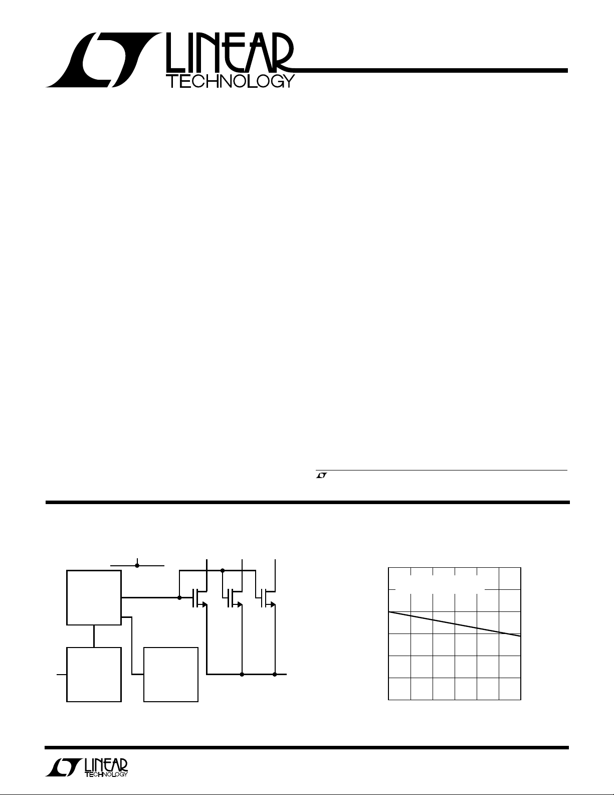
SI PLIFIED BLOCK DIAGRAM
EN
GATE CHARGE
AND
DISCHARGE
CONTROL LOGIC
CHARGE
PUMP
*NMOS SWITCHES WITH NO PARASITIC BODY DIODES
V
INS
CURRENT LIMIT
AND THERMAL
SHUTDOWN
V
IN1
***
V
IN2
, LTC and LT are registered trademarks of Linear Technology Corporation.
WW
V
IN3
V
OUT
LTC1477/1478 • TA01
5.20
5.10
5.00
4.90
4.80
OUTPUT VOLTAGE (V)
4.70
4.60
Switch Output Voltage
TA = 25°C
= V
V
0
= V
IN1
IN2
0.5 0.75 1.00
0.25
OUTPUT CURRENT (A)
IN3
= V
INS
= 5V
1.25 1.50
LTC1477/1478 • TP02
1
Page 2
LTC1477/LTC1478
WW
W
U
ABSOLUTE MAXIMUM RATINGS
Supply Voltage .......................................................... 7V
Enable Input Voltage...................... (7V) to (GND –0.3V)
Output Voltage (OFF) (Note 1) .......(7V) to (GND –0.3V)
Output Short-Circuit Duration.......................... Indefinite
Junction Temperature...........................................110°C
U
W
PACKAGE/ORDER INFORMATION
ORDER PART
NUMBER
LTC1477CS8
S8 PART MARKING
1477
V
1
OUT
V
2
IN1
V
3
INS
EN
4
8-LEAD PLASTIC SO
T
= 110°C, θJA = 120°C/W
JMAX
TOP VIEW
S8 PACKAGE
V
8
OUT
V
7
IN2
V
6
IN3
GND
5
Operating Temperature
LTC1477C/LTC1478C ..............................0°C to 70°C
Storage Temperature Range ................. –65°C to 150°C
Lead Temperature (Soldering, 10 sec)..................300°C
U
1
AV
OUT
2
AV
IN
3
AV
INS
4
AEN
5
GND
6
BV
IN3
7
BV
IN2
8
BV
OUT
16-LEAD PLASTIC SO
T
JMAX
TOP VIEW
16
15
14
13
12
11
10
9
S PACKAGE
= 110°C, θJA = 100°C/ W
AV
AV
AV
GND
BEN
BV
BV
BV
OUT
IN2
IN3
INS
IN1
OUT
ORDER PART
NUMBER
LTC1478CS
Consult factory for Industrial and Military grade parts.
ELECTRICAL CHARACTERISTICS
V
= V
= V
= V
INS
IN1
IN2
SYMBOL PARAMETER CONDITIONS MIN TYP MAX UNITS
V
IN
I
VIN
R
ON
I
LKG
I
SC
V
ENH
V
ENL
I
EN
t
D+R
The
Supply Voltage Range 2.7 5.5 V
Supply Current Switch OFF, Enable = 0V ● 0.01 10 µA
ON Resistance V
Output Leakage Current OFF Switch OFF, Enable = 0V ● ±20 µA
Short-Circuit Current Limit V
Enable Input High Voltage 3.0V ≤ V
Enable Input Low Voltage 3.0V ≤ V
Enable Input Current 0V ≤ VEN ≤ 5.5V ● ±1 µA
Delay and Rise Time R
● denotes specifications which apply over the full operating
temperature range.
Note 1: The V
Note 2: The V
pins are typically connected to V
V
IN3
pins must be connected together.
OUT
and V
INS
selectively disconnected to reduce the short-circuit current limit and
= 5V (Note 2), TA = 25°C, unless otherwise noted. Each channel of the LTC1478 is tested separately (Note 3).
IN3
Switch ON, Enable = 5V, VIN = 5V ● 120 180 µA
Switch ON, Enable = 3.3V, VIN = 3.3V ● 80 120 µA
= V
= V
= V
INS
V
INS
V
INS
V
INS
INS
V
INS
OUT
IN1
= V
= V
= V
= V
= V
IN2
= V
IN1
IN2
= 5V, V
IN1
= 3.3V, V
IN1
= V
IN1
IN2
= 5V, V
IN1
≤ 5.5V ● 2.0 V
INS
≤ 5.5V ● 0.8 V
INS
= 100Ω, C
= 5V, I
IN3
= V
= 3.3V, I
IN3
= V
IN2
IN3
= V
IN2
= V
= 5V, V
IN3
= V
IN2
IN3
= 1µF, to 90% of Final Value 0.50 1.00 2.00 ms
OUT
= 1A 0.07 0.12 Ω
OUT
= 1A 0.08 0.12 Ω
OUT
= NC, I
= NC, I
IN3
= NC, V
= 0.5A 0.12 0.20 Ω
OUT
= 0.5A 0.13 0.20 Ω
OUT
= 0V, (Note 4) 1.60 2.00 2.40 A
OUT
= 0V, (Note 4) 0.68 0.85 1.02 A
OUT
increase the ON resistance of the switch. The LTC1478 GND pins must be
connected together. (See Pin Functions and Block Diagram for more detail.)
Note 3: Other channel turned OFF, i.e. AEN and BEN = 0V.
pins must be connected together. The V
IN1
INS
and V
pins but can be
IN1
IN2
and
Note 4: The output is protected with fold-back current limit which reduces
the short-circuit (0V) currents below peak permissible current levels at
higher output voltages. (See Typical Performance Characteristics for
further detail on output current versus output voltage).
2
Page 3
W
JUNCTION TEMPERATURE (°C)
0
0
SWITCH RESISTANCE (Ω)
0.05
0.10
0.15
0.20
0.25
0.30
25 50 75 100
LTC1477/1478 • TPC03
125
V
INS
= V
IN1
= 5V
V
IN2
= V
IN3
= NC
ALL VIN PINS = 5V
OUTPUT VOLTAGE (V)
0
0
OUTPUT CURRENT (A)
1
2
3
4
6
1
234
LTC1477/1478 • TPC06
56
5
TA = 25°C
ALL VIN PINS = 5V
V
IN2
= V
IN3
= NC
TIME (ms)
–0.4
INRUSH CURRENT (A)OUTPUT VOLTAGE (V)
0
1
2.8
LTC1477/1478 • TPC09
6
4
0
0.4
1.2
2.0
2
3
2
0
0.8
1.6
2.4
C
OUT
= 470µF
R
OUT
= 10Ω
C
OUT
= 10µF
R
OUT
= 10Ω
CURRENT
LIMITED
TJ = 25°C
ALL V
IN
PINS = 3.3V
U
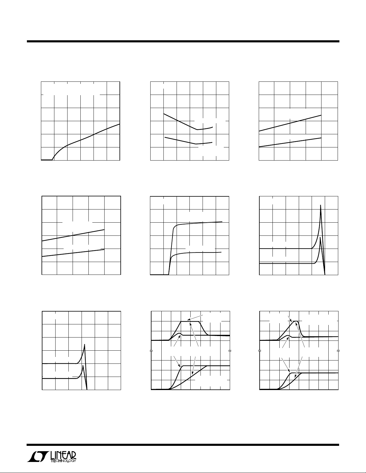
TYPICAL PERFORMANCE CHARACTERISTICS
LTC1477/LTC1478
Supply Current (ON) Switch Resistance
300
TA = 25°C
OUTPUT TURNED ON, NO LOAD
250
200
150
100
SUPPLY CURRENT (µA)
50
0
0
1
SUPPLY VOLTAGE (V)
234
LTC1477/1478 • TPC01
56
SWITCH RESISTANCE (Ω)
0.30
0.25
0.20
0.15
0.10
0.05
0
TA = 25°C
1
2
Switch Resistance (3.3V) Short-Circuit Current
SWITCH RESISTANCE (Ω)
0.30
0.25
0.20
0.15
0.10
0.05
V
= V
= 3.3V
INS
IN1
= V
V
= NC
IN2
IN3
ALL VIN PINS = 3.3V
3.0
TJ = 25°C
2.5
2.0
1.5
1.0
SHORT-CIRCUIT CURRENT (A)
0.5
V
= V
IN2
ALL VIN PINS
CONNECTED
345
INPUT VOLTAGE (V)
ALL VIN PINS
CONNECTED
V
= V
IN2
IN3
= NC
IN3
67
LTC1477/1478 • TPC02
= NC
Switch Resistance (5V)
Output Current (5V)
0
6
5
4
3
2
OUTPUT CURRENT (A)
1
0
0
25 50 75 100
JUNCTION TEMPERATURE (°C)
125
LTC1477/1478 • TPC04
0
0
234
1
SUPPLY VOLTAGE (V)
Output Current (3.3V) Inrush Current (5V)
TA = 25°C
ALL VIN PINS = 3.3V
V
= V
= NC
IN2
IN3
0
234
1
OUTPUT VOLTAGE (V)
56
LTC1477/1478 • TPC07
3
2
1
0
INRUSH CURRENT (A)OUTPUT VOLTAGE (V)
6
4
2
0
–0.4
C
= 10µF
OUT
= 10Ω
R
OUT
0
0.4
1.2
0.8
TIME (ms)
C
OUT
R
OUT
LTC1477/1478 • TPC05
CURRENT
LIMITED
= 470µF
= 10Ω
TJ = 25°C
ALL V
IN
1.6
56
PINS = 5V
2.0
2.4
LTC1477/1478 • TPC08
Inrush Current (3.3V)
2.8
3
Page 4

LTC1477/LTC1478
UUU
PIN FUNCTIONS
LTC1477
EN (Pin 4): The enable input is a high impedance CMOS
gate with an ESD protection diode to ground and should
not be forced below ground. This input has about 100mV
of built-in hysteresis to ensure clean switching.
V
, V
INS
connected to the V
V
INS
(Pins 3,2): The V
IN1
supply pin (see Block Diagram). The
IN1
supply pin provides power for the input control logic,
the current limit and thermal shutdown circuitry; plus
provides a sense connection to the input power supply.
The gate of the NMOS switch is powered by a charge pump
from the V
supply pin (see Block Diagram). The V
INS
supply pin provides connection to the drain of 1/2 of the
output power device.
V
, V
IN2
typically tied to the V
(Pins 7,6): The V
IN3
INS
and V
resistance; i.e., when all four VIN pins are connected
together the entire power device is connected (see Block
Diagram). Each auxiliary supply pin, V
connected to the drain of 1/4 of the power device. The V
and V
pins can be selectively disconnected to reduce
IN3
the short-circuit current limit at the expense of higher
R
. (See Applications Information section for more
DS(ON)
details.)
V
(Pins 1,8): The output pins of the LTC1477 must
OUT
always be tied together. The output is protected against
accidental short circuits to ground by a current limit circuit
which protects the system power supply and load against
damage. A second level of protection is provided by
thermal shutdown circuitry which limits the die temperature to 130°C.
supply pin must always be
INS
and V
IN2
supply pins for lowest ON
IN1
supply pins are
IN3
and V
IN2
IN3
IN1
, is
IN2
LTC1478
AEN, BEN (Pins 4,12): The enable inputs are high imped-
ance CMOS gates with ESD protection diodes to ground
and should not be forced below ground. These inputs
have about 100mV of built-in hysteresis to ensure clean
switching.
AV
, AV
INS
or BV
INS
AV
or BV
IN1
and BV
logic, the current limit and thermal shutdown circuitry;
plus, provides a sense connection to the input power
supply. The gate of the NMOS switch is powered by a
charge pump from the AV
Block Diagram). The AV
connection to the drain of 1/2 of the output power device.
AV
, AV
IN2
AV
, BV
IN3
AV
, AV
INS
resistance; i.e., when all four AVIN, BV
nected together the entire power device is connected (see
Block Diagram). Each auxiliary supply pin, AV
BV
and BV
IN2
mately 1/4 of the corresponding power device. The AV
AV
, BV
IN3
nected to reduce the short-circuit current limit at the
expense of higher R
section for more details.)
AV
, BV
OUT
are protected against accidental short circuits to ground
by a current limit circuit which protects the system power
supplies and loads against damage. A second level of
protection is provided by thermal shutdown circuitry
which limits the die temperature to approximately 130°C.
IN1
, BV
INS
, BV
(Pins 3,2; 11,10): The AV
IN1
supply pin must always be connected to the
supply pin (see Block Diagram). The AV
IN1
supply pins provide power for the input control
INS
and BV
INS
and BV
IN1
IN3
and BV
IN2
IN1
IN2
OUT
, BV
, BV
, BV
IN2
IN3
INS
, is connected to the drain of approxi-
IN3
and BV
DS(ON)
, (Pins 15,14; 7,6): The AV
IN3
supply pins are typically tied to the
and BV
pins can be selectively discon-
IN3
supply pins for lowest ON
IN1
. (See Applications Information
(Pins 1,16; 8,9): The outputs of the LTC1478
supply pins (see
INS
supply pins provide
IN1
pins are con-
IN
, AV
IN2
IN2
IN3
IN2
INS
INS
,
,
,
4
Page 5

U
OPERATION
LTC1477/LTC1478
(LTC1477 or single channel of LTC1478)
Input TTL-CMOS Converter
The LTC1477 enable input is designed to accommodate a
wide range of 3V and 5V logic families. The input threshold
voltage is approximately 1.4V with 100mV of hysteresis.
The input enables the bias generator, the gate charge
pump and the protection circuitry. Therefore, when the
enable input is turned off, the entire circuit is powered
down and the supply current drops below 1µA.
Ramped Switch Control
The LTC1477 gate charge pump includes circuitry which
ramps the NMOS switch on slowly (1ms typical rise time)
but turns it off much more quickly (typically 20µs).
Bias, Oscillator and Gate Charge Pump
When the switch is enabled, a bias current generator and
high frequency oscillator are turned on. The on-chip
capacitive charge pump generates approximately 12V of
gate drive for the internal low R
NMOS switch from
DS(ON)
the power supply. No external 12V supply is required to
switch the output.
Switch Protection
Two levels of protection are designed into the power
switch in the LTC1477. The switch is protected against
accidental short circuits with a current limit circuit which
limits the output current to typically 2A when the output is
shorted to ground. The LTC1477 also has thermal shutdown set at approximately 130°C which limits the power
dissipation to safe levels.
LTC1478 Operation
The LTC1478 dual protected switch can be thought of as
two independent LTC1477 single protected switches. The
input supply voltages may be from separate power sources.
The ground connection, however, is common to both
channels and must be connected to the same potential.
W
BLOCK DIAGRAM
TTL-TO-CMOS
EN
CONVERTER
(LTC1477 or single channel of LTC1478)
V
INS
GATE CHARGE
AND
DISCHARGE
CONTROL LOGIC
OSCILLATOR
AND BIAS
U
WUU
CHARGE
PUMP
APPLICATIONS INFORMATION
Tailoring I
The LTC1477 is designed to current limit at approximately
2A during a short circuit with all the VIN pins connected to
the input power supply. It is possible however, to reduce
this current by selectively disconnecting two of the four
power supply pins (V
of disconnecting these pins on R
current limit
LIMIT
and R
DS(ON)
and V
IN2
for Load Requirements
). Table 1 lists the effects
IN3
and short-circuit
DS(ON)
V
IN1
CURRENT LIMIT
AND THERMAL
SHUTDOWN
Table 1. Effects of Disconnecting V
ALL VIN PINS V
CONNECTED DISCONNECTED DISCONNECTED
R
DS(ON)
I
LIMIT
Note: 5V Operation
0.07Ω 0.09Ω 0.12Ω
2A 1.5A 0.85A
V
IN2
IN3
V
IN3
V
OUT
LTC1477/1478 • BD01
and V
IN2
V
IN3
IN2
AND V
IN3
Note that there is an inverse relationship between output
current limit and switch resistance. This allows the tailor-
5
Page 6

LTC1477/LTC1478
+
1µF
0.1µF
LTC1477/1478 • TA04
ON/OFF
2.7V TO 5.5V
ISC = 1.5A
NC
LTC1477
V
OUT
V
IN2
V
IN3
GND
V
OUT
V
IN1
V
INS
EN
U
WUU
APPLICATIONS INFORMATION
ing of the switch parameters to the expected load current
and system current limit requirements.
A couple of examples are helpful:
1. If a nominal load of 1A was controlled by the switch
configured to current limit at 2A (all VIN pins connected
together), the R
drop across the switch would be 70mV. The power
dissipated by the switch would only be 70mW.
2. If a nominal load of 0.5A was controlled by the switch
configured to current limit at 0.85A (V
disconnected), the R
But the voltage drop would remain at 70mV and the
switch power dissipation would drop to 35mW.
Supply Bypassing
For best results, bypass the supply input pins with a single
1.0µ F capacitor as close as possible to the LTC1477.
Sometimes, much larger capacitors are already available
at the output of the power supply. In this case, it is still
good practice to use a 0.1µ F capacitor as close as possible
would be 0.07Ω and the voltage
DS(ON)
would increase to 0.14Ω.
DS(ON)
IN2
and V
IN3
to the LTC1477, especially if the power supply output
capacitor is more than 2 inches away on the printed circuit
board.
Output Capacitor
The output pin is designed to ramp on slowly, typically
1ms rise time. Therefore, very large output capacitors can
be driven without producing voltage spikes on the supply
pins (see graphs in Typical Performance Characteristics).
The output pin should have a 1µF capacitor for noise
reduction and smoothing.
Supply and Input Sequencing
The LTC1477 is designed to operate with continuous
power (quiescent current drops to < 1µ A when disabled).
If the power must be turned off, for example to enter a
system “sleep” mode, the enable input must be turned off
100µ s before the input supply is turned off to ensure that
the gate of the NMOS switch is completely discharged
before power is removed. However, the input control and
power can be applied simultaneously during power up.
TYPICAL APPLICATIONS
2A Protected Switch 1.5A Protected Switch
2.7V TO 5.5V
2.7V TO 5.5V
6
0.1µF
0.1µF
ON/OFF
ON/OFF
V
OUT
V
IN1
LTC1477
V
INS
EN
0.85A Protected Switch 2A Protected Switch Driving a Large Capacitive Load
V
OUT
V
IN1
LTC1477
V
INS
EN
V
U
V
OUT
V
IN2
V
IN3
GND
OUT
V
IN2
V
IN3
GND
+
LTC1477/1478 • TA03
+
NC
NC
LTC1477/1478 • TA05
ISC = 2A
1µF
= 0.85A
I
SC
1µF
2.7V TO 5.5V
0.1µF
ON/OFF
V
OUT
V
OUT
V
IN1
V
INS
EN
LTC1477
V
V
V
GND
OUT
IN2
IN3
+
C
LOAD
100µF
LTC1477/1478 • TA06
Page 7

U
TYPICAL APPLICATIONS
Adding Short-Circuit Protection to an LT1301 Step-Up Switching Regulator (0.01µA Standby Current)
5V
0.1µF
V
OUT
V
IN1
LTC1477
V
INS
ON/OFF
EN
*COILCRAFT DO1608-103
5V to 3.3V Selector Switch with Slope Control and 0.01µA Standby Current
V
V
V
GND
OUT
IN2
IN3
LTC1477/LTC1478
L1*
10µH
+
100µF
10V
V
IN
24
SEL
LT1301
3
SHDN
PGND
76
SW
SENSE
I
LIM
GND
18
D1
MBRS130LT3
+
0.1µF
NC
DN117 • F03
5
12V
47µF
16V
TANT
+
SINGLE
Li-Ion
CELL*
5V
0.1µF
5V ON/OFF*
3.3V
0.1µF
3.3V ON/OFF*
*ALLOW AT LEAST 100ms BETWEEN 5V AND 3.3V SWITCHING FOR DISCHARGE OF 100µF OUTPUT CAPACITOR
AV
AV
AV
AEN
GND
BV
BV
BV
OUT
IN1
INS
IN3
IN2
OUT
LTC1478
AV
BV
AV
AV
BV
BV
OUT
IN2
IN3
GND
BEN
INS
IN1
OUT
1k
LTC1477/1478 • TA08
Single Li-Ion Cell to 5V Converter/Switch with Load Disconnect Below 2.7V
22µH
100µF
16V
562k
1%
432k
1%
220k
SUMIDA
CD54-220
34
V
IN
6
I
LIM
LT1304CS8-5
1
LBI
7
SHDN
SENSENC
5
MBRS130LT3
SW
8
2
LBO
(5V)(2.7V to 4.2V)
V
OUT
V
100µF
+
10V
TANT
IN1
V
INS
EN
LTC1477
LTC1477/1478 • TA09
V
OUT
V
IN2
V
IN3
GND
5V/2A OR
3.3V/2A
+
100µF
10V
5V
+
1µF
NC
NC
*PRIMARY Li-Ion BATTERY PROTECTION MUST BE PROVIDED BY AN INDEPENDENT CIRCUIT
Information furnished by Linear Technology Corporation is believed to be accurate and reliable.
However, no responsibility is assumed for its use. Linear Technology Corporation makes no representation that the interconnection of its circuits as described herein will not infringe on existing patent rights.
7
Page 8

LTC1477/LTC1478
PACKAGE DESCRIPTION
0.010 – 0.020
(0.254 – 0.508)
0.008 – 0.010
(0.203 – 0.254)
*
DIMENSION DOES NOT INCLUDE MOLD FLASH. MOLD FLASH
SHALL NOT EXCEED 0.006" (0.152mm) PER SIDE
**
DIMENSION DOES NOT INCLUDE INTERLEAD FLASH. INTERLEAD
FLASH SHALL NOT EXCEED 0.010" (0.254mm) PER SIDE
× 45°
0.016 – 0.050
0.406 – 1.270
0.053 – 0.069
(1.346 – 1.752)
0°– 8° TYP
U
Dimension in inches (millimeters) unless otherwise noted.
S8 Package
8-Lead Plastic Small Outline (Narrow 0.150)
(LTC DWG # 05-08-1610)
0.004 – 0.010
(0.101 – 0.254)
0.228 – 0.244
0.014 – 0.019
(0.355 – 0.483)
0.050
(1.270)
BSC
S Package
16-Lead Plastic Small Outline (Narrow 0.150)
(LTC DWG # 05-08-1610)
16
15
(5.791 – 6.197)
0.386 – 0.394*
(9.804 – 10.008)
13
14
12
11 10
0.189 – 0.197*
(4.801 – 5.004)
7
8
1
2
5
6
0.150 – 0.157**
(3.810 – 3.988)
3
9
SO8 0695
4
0.228 – 0.244
(5.791 – 6.197)
3
2
0.010 – 0.020
(0.254 – 0.508)
0.008 – 0.010
(0.203 – 0.254)
*
DIMENSION DOES NOT INCLUDE MOLD FLASH. MOLD FLASH
SHALL NOT EXCEED 0.006" (0.152mm) PER SIDE
**
DIMENSION DOES NOT INCLUDE INTERLEAD FLASH. INTERLEAD
FLASH SHALL NOT EXCEED 0.010" (0.254mm) PER SIDE
× 45°
0° – 8° TYP
0.016 – 0.050
0.406 – 1.270
1
0.053 – 0.069
(1.346 – 1.752)
0.014 – 0.019
(0.355 – 0.483)
4
RELATED PARTS
PART NUMBER DESCRIPTION COMMENTS
LTC1153 Electronic Circuit Breaker MOSFET Driver with Adjustable Reset Time
LTC1154 Single High Side Driver MOSFET Driver with Switch Status Output
LTC1155 Dual High Side Driver Dual MOSFET Driver with Protection
TM
LTC1470 5V and 3.3V VCC Switch SafeSlot
LTC1471 Dual 5V and 3.3V VCC Switch Dual Version of LTC1470 in 16-Lead SO
LTC1472 PCMCIA VCC and VPP Switches Complete Single Channel SafeSlot Protection
SafeSlot is a trademark of Linear Technology Corporation.
Protected Switch in 8-Lead SO
5
0.050
(1.270)
TYP
0.150 – 0.157**
(3.810 – 3.988)
7
6
8
0.004 – 0.010
(0.101 – 0.254)
S16 0695
8
Linear Technology Corporation
1630 McCarthy Blvd., Milpitas, CA 95035-7417
(408) 432-1900
●
FAX
: (408) 434-0507
●
TELEX
: 499-3977
LT/GP 0995 10K • PRINTED IN USA
LINEAR TECHNOLOGY CORPORATION 1 995
 Loading...