

Page 1
FEATURES
PowerPath
DESCRIPTIO
LTC1473L
Dual Low Voltage
TM
Switch Driver
U
■
Power Path Management for Systems
with Multiple DC Sources
■
Switches and Isolates Sources from 3.3V to 10V
■
All N-Channel Switching to Reduce Power Losses
and System Cost
■
Built-In Step-Up Regulator for N-Channel Gate Drive
■
Capacitor Inrush and Short-Circuit Current Limited
■
User-Programmable Timer Prevents Overdissipation
During Current Limiting
■
Undervoltage Lockout Prevents Operation with Low
Inputs
■
Small Footprint: 16-Pin Narrow SSOP
U
APPLICATIO S
■
Portable Computers
■
Portable Instruments
■
Fault Tolerant Computers
■
Battery-Backup Systems
■
3.3V/5V Power Management
The LTC®1473L provides reliable and efficient switching
between two DC power sources. This device drives two
external sets of back-to-back N-channel MOSFET switches
to route power to the input of a low voltage system. An
internal boost regulator provides the voltage to fully enhance the logic-level N-channel MOSFET switches while
an internal undervoltage lock-out circuit keeps the system
alive down to 2.8V.
The LTC1473L senses current to limit inrush between the
batteries and the system supply capacitor during switchover transitions or during fault conditions. A user-programmable timer monitors the time the MOSFET switches
are in current limit and latches them off when the programmed time is exceeded.
A unique “2-diode” logic mode ensures system start-up
regardless of which input receives power first.
, LTC and LT are registered trademarks of Linear Technology Corporation.
PowerPath is a trademark of Linear Technology Corporation.
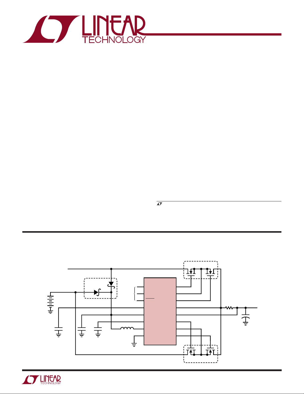
TYPICAL APPLICATIO
DCIN
3.3V
V
BAT1
4× NiMH
C
TIMER
2000pF
1µF
* COILCRAFT 1812LS-105XKBC
BAT54C
U
1µF
3.3V to 4-Cell NiMH Backup Switch
LOGIC
DRIVEN
1mH*
1
2
3
4
5
6
7
8
IN1
IN2
DIODE
TIMER
+
V
V
GG
SW
GND
LTC1473L
GA1
SAB1
GB1
SENSE
SENSE
GA2
SAB2
GB2
16
15
14
13
+
12
–
11
10
9
Si9926DY
Si9926DY
R
SENSE
0.04Ω
1473 TA01
3.3V OR
V
+
BAT1
C
OUT
1
Page 2
LTC1473L
WW
W
ABSOLUTE AXI U RATI GS
(Note 1)
SENSE+, SENSE–, V+..................................–0.3 to 10V
GA1, GB1, GA2, GB2 ...................................–0.3 to 20V
SAB1, SAB2.................................................–0.3 to 10V
SW, VGG......................................................–0.3 to 20V
IN1, IN2, DIODE...........................................–0.3V to 7V
Junction Temperature (Note 2).............................125°C
Operating Temperature Range.....................0°C to 70°C
Storage Temperature Range................. –65°C to 150°C
Lead Temperature (Soldering, 10 sec)..................300°C
U
UUW
PACKAGE/ORDER I FOR A TIO
TOP VIEW
IN1
1
IN2
2
DIODE
3
TIMER
4
+
V
5
V
6
GG
SW
7
GND
8
GN PACKAGE
16-LEAD NARROW PLASTIC SSOP
T
= 125°C, θJA = 150°C/W
JMAX
16
15
14
13
12
11
10
9
GA1
SAB1
GB1
SENSE
SENSE
GA2
SAB2
GB2
+
–
ORDER PART
NUMBER
LTC1473LCGN
GN PART MARKING
1473L
Consult factory for Military and Industrial grade parts.
ELECTRICAL CHARACTERISTICS
The ● denotes the specifications which apply over the full operating
temperature range, otherwise specifications are at TA = 25°C. Test circuit, V+ = 5V, unless otherwise specified.
SYMBOL PARAMETER CONDITIONS MIN TYP MAX UNITS
+
V
I
S
V
GS
+
V
UVLO
+
V
UVLOHYS
V
HIDIGIN
V
LODIGIN
I
IN
V
GS(ON)
V
GS(OFF)
I
BSENSE
I
BSENSE
V
SENSE
I
PDSAB
I
TIMER
V
TIMER
t
ON
t
OFF
t
D1
t
D2
f
OVGG
Supply Operating Range 2.8 9 V
Supply Current V
IN1
= V
DIODE
= 5V, V
IN2
= 0V, V
SENSE
+
= V
–
= 5V ● 100 200 µA
SENSE
VGS Gate Supply Voltage VGS = VGG – V+, 2.8V ≤ V+ ≤ 10V (Note 3) ● 7.5 8.5 9.5 V
V+ Undervoltage Lockout Threshold V+ Ramping Down ● 2.3 2.5 2.8 V
V+ Undervoltage Lockout Hysteresis 70 mV
Digital Input Logic High (Note 4) ● 2 0.9 V
Digital Input Logic Low (Note 4) ● 0.6 0.4 V
Input Current V
Gate-to-Source ON Voltage I
Gate-to-Source OFF Voltage I
+
SENSE+ Input Bias Current V
–
SENSE– Input Bias Current V
Inrush Current Limit Sense Voltage V
SAB1, SAB2 Pull-Down Current V
Timer Source Current V
Timer Latch Threshold Voltage V
Gate Drive Rise Time C
Gate Drive Fall Time C
Gate Drive Turn-On Delay C
Gate Drive Turn-Off Delay C
= V
IN1
= I
GA1
= I
GA1
SENSE
V
SENSE
SENSE
V
SENSE
SENSE–
V
SENSE–
= V
IN1
= V
V
IN1
= 0.4V, V
IN1
V
SENSE
= 0.4V, V
IN1
= 1000pF, V
GS
= 1000pF, V
GS
= 1000pF, V
GS
= 1000pF, V
GS
= V
IN2
= I
GA2
= I
GA2
+
= V
SENSE
+
= V
SENSE
+
= V
SENSE–
+
= V
SENSE
= 10V (V
= 0V (V
= V
IN2
= 0.4V, V
IN2
+
– V
SENSE
= 5V ±1 µA
DIODE
= I
GB1
GB1
DIODE
IN2
IN2
= –1µA, V
GB2
= I
= 100µA, V
GB2
–
= 10V (Note 3) ● 24.510µA
–
= 0V (Note 5) ● –300 –175 –75 µA
= 10V (Note 3) ● 24.510µA
–
= 0V (Note 5) ● –300 –175 –75 µA
– V
SENSE+
SENSE+
– V
SENSE
SENSE
= 0.4V, V+ = 10V (Note 3) 5 20 35 µA
= 2V 30 140 300 µA
DIODE
= V
= V
SAB1
SAB1
SAB1
SAB1
= 2V, V
DIODE
–
= 300mV
= 2V ● 1.05 1.16 1.25 V
DIODE
= V
= 0V (Note 6) 33 µs
SAB2
= V
= 5V (Note 6) 2 µs
SAB2
= V
= 0V (Note 6) 22 µs
SAB2
= V
= 5V (Note 6) 1 µs
SAB2
= V
SAB1
SAB1
–
) (Note 3) 0.15 0.20 0.25 V
–
) 0.10 0.20 0.30 V
TIMER
= 5V ● 4.5 5.6 7.0 V
SAB2
= V
= 5V ● 0 0.4 V
SAB2
= 0V, ● 369µA
VGS Regulator Operating Frequency 30 kHz
2
Page 3
ELECTRICAL CHARACTERISTICS
LTC1473L
Note 1: Absolute Maximum Ratings are those values beyond which the life
of a device may be impaired.
Note 2: T
dissipation P
is calculated from the ambient temperature TA and power
J
according to the following formula:
D
TJ = TA + (PD)(150°C/W)
Note 3: Some tests are performed under more stringent conditions to
ensure reliable operation over the entire supply voltage range.
Note 4: Digital inputs include: IN1, IN2 and DIODE.
Note 5: I
increases by the same amount as I
S
their common mode falls below 5V.
Note 6: Gate turn-on and turn-off times are measured with no inrush
current limiting, i.e., V
4.5V and fall times are measured from 4.5V to 1V. Delay times are
measured from the input transition to when the gate voltage has risen or
fallen to 3V. Results are not tested, but guaranteed by design.
UW
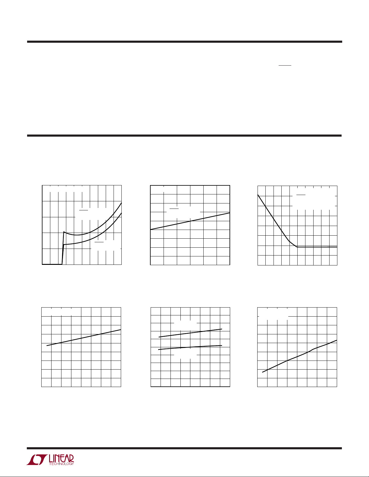
TYPICAL PERFOR A CE CHARACTERISTICS
DC Supply Current
vs Supply Voltage
250
200
150
100
SUPPLY CURRENT (µA)
50
0
0
V
SENSE
+
= V
2 45678913
+
–
= V
SENSE
V
= V
DIODE
IN1
V
IN2
V
DIODE
V
IN1
SUPPLY VOLTAGE (V)
= 5V
= 0V
= V
= 5V
IN2
= 0V
10
1473 G01
DC Supply Current
vs Temperature
140
V+ = 5V
130
120
110
100
90
80
SUPPLY CURRENT (µA)
70
60
50
–25 25 50 75 100
–50
V
= V
DIODE
TEMPERATURE (°C)
= 5V
IN1
V
= 0V
IN2
0
1473 G02
+
+ I
BSENSE
= 0V. Gate rise times are measured from 1V to
SENSE
DC Supply Current vs V
400
350
300
250
200
150
SUPPLY CURRENT (µA)
100
50
0
0
V
V+ = 5V
V
DIODE
V
IN2
V
SENSE
567 101234 89
COMMON MODE (V)
SENSE
BSENSE
= V
= 0V
+
– V
–
when
SENSE
= 5V
IN1
SENSE
–
= 0V
1473 G03
VGS Gate-to-Source ON Voltage
vs Temperature
6.0
V+ = V
= 10V
5.9
5.8
5.7
5.6
5.5
5.4
5.3
GATE-TO-SOURCE ON VOLTAGE (V)
GS
5.2
V
5.1
SAB
–60–40–20 204060800
TEMPERATURE (°C)
1473 G04
100
Undervoltage Lockout Threshold (V+)
vs Temperature
2.75
2.70
2.65
2.60
2.55
2.50
2.45
2.40
2.35
2.30
UNDERVOLTAGE LOCKOUT THRESHOLD (V)
2.25
–60
–40 0
START-UP
THRESHOLD
SHUTDOWN
THRESHOLD
–20
20
TEMPERATURE (°C)
40
VGS Gate Supply Voltage
vs Temperature
9.0
V+ = 5V
= VGG – V
V
8.9
GS
8.8
8.7
8.6
8.5
8.4
GATE SUPPLY VOLTAGE (V)
8.3
GS
V
8.2
80
60
100
1473 G05
8.1
–40–60
+
–20 20406080100
0
TEMPERATURE (°C)
1473 G06
3
Page 4
LTC1473L
UW
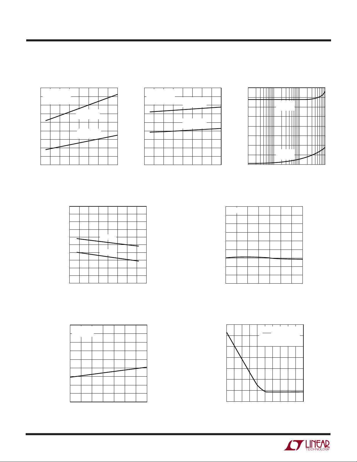
TYPICAL PERFOR A CE CHARACTERISTICS
Turn-Off Delay and Gate Fall Time
vs Temperature
2.2
+
= 5V
V
= 1000pF
C
2.0
LOAD
V
= 5V
SAB
1.8
1.6
1.4
1.2
1.0
0.8
0.6
TURN-OFF DELAY AND GATE FALL TIME (µs)
0.4
–20 20406080100
–40–60
GATE FALL
TIME
TURN-OFF
DELAY
0
TEMPERATURE (°C)
Logic Input Threshold Voltage
vs Temperature
2.0
1.8
1.6
1.4
1.2
1.0
0.8
0.6
0.4
INPUT THRESHOLD VOLTAGE (V)
0.2
0
–60
–40 0
–20
TEMPERATURE (°C)
1473 G07
V+ = 10V
V+ = 2.8V
20
Turn-On Delay and Gate Rise Time
vs Temperature
45
+
= 5V
V
40
35
30
25
20
15
10
5
TURN-ON DELAY AND GATE RISE TIME (µs)
0
= 1000pF
C
LOAD
V
= 0V
SAB
–40 –20 20 40 60 80 100
–60
TEMPERATURE (°C)
GATE RISE
TIME
TURN-ON
DELAY
0
1473 G08
Rise and Fall Time
vs Gate Capacitive Loading
40
35
30
25
20
15
10
RISE AND FALL TIME (µs)
5
0
10
RISE TIME
= 0V
V
SAB
FALL TIME
= 5V
V
SAB
100 1000 10000
GATE CAPACITIVE LOADING (pF)
1473 G08
Timer Latch Threshold Voltage
vs Temperature
1.28
V+ = 5V
1.26
1.24
1.22
1.20
1.18
1.16
1.14
1.12
TIMER LATCH THRESHOLD VOLTAGE (V)
80
60
40
100
1473 G10
1.10
–25 25 50 75 100 125
–50
0
TEMPERATURE (°C)
1473 G11
4
Timer Source Current
vs Temperature
8.5
V+ = 5V
TIMER = 0V
8.0
7.5
7.0
6.5
6.0
5.5
5.0
TIMER SOURCE CURRENT (µA)
4.5
4.0
–25 25 50 75 100 125
–50
0
TEMPERATURE (°C)
1473 G12
SENSE Pin Source Current
(I
300
250
200
150
100
50
SENSE PIN CURRENT (µA)
0
–50
0
) vs V
BSENSE
123456789
SENSE
V+ = 5V
V
V
V
V
SENSE
DIODE
= 0V
IN2
SENSE
(V)
= V
+
– V
IN1
SENSE
= 5V
–
= 0V
10
1473 G13
Page 5
UUU
PI FU CTIO S
LTC1473L
IN1 (Pin 1): Logic Input of Gate Drivers GA1 and GB1. IN1
is disabled when IN2 is high or DIODE is low. During
2-diode mode, asserting IN1 disables the fault timer
function.
IN2 (Pin 2): Logic Input of Gate Drivers GA2 and GB2. IN2
is disabled when IN1 is high or DIODE is low. During
2-diode mode, asserting IN2 disables the fault timer
function.
DIODE (Pin 3): “2-Diode Mode” Logic Input. Diode overrides IN1 and IN2 by forcing the two back-to-back
external N-channel MOSFET switches to mimic two diodes.
TIMER (Pin 4): Fault Timer. A capacitor connected from
this pin to GND programs the time the MOSFET switches
are allowed to be in current limit. To disable this function,
Pin 4 can be grounded.
V+ (Pin 5): Power Supply. Bypass this pin with at least a
1µF capacitor.
VGG (Pin 6): Gate Driver Supply. This high voltage supply
is intended only for driving the internal micropower gate
drive circuitry.
circuitry
. Bypass this pin with at least 1µF.
Do not load this pin with any external
SW (Pin 7): Open Drain of an Internal N-Channel MOSFET
Switch. This pin drives the bottom of the VGG switching
regulator inductor which is connected between this pin and
the V+ pin.
GND (Pin 8): Ground.
GB2, GA2 (Pins 9, 11): Switch Gate Drivers. GA2 and GB2
drive the gates of the second back-to-back external
N-channel switches.
SAB2 (Pin 10): Source Return. The SAB2 pin is connected
to the sources of SW A2 and SW B2. A small pull-down
current source returns this node to 0V when the switches
are turned off.
SENSE– (Pin 12): Inrush Current Input. This pin should be
connected directly to the bottom (output side) of the low
valued resistor in series with the two input power selector
switch pairs, SW A1/B1 and SW A2/B2, for detecting and
controlling the inrush current into and out of the power
supply sources and the output capacitor.
SENSE+ (Pin 13): Inrush Current Input. This pin should be
connected directly to the top (switch side) of the low
valued resistor in series with the two input power selector
switch pairs, SW A1/B1 and SW A2/B2, for detecting and
controlling the inrush current into and out of the power
supply sources and the output capacitor. Current limit is
invoked when (V
Pin Function Table
PIN NAME DESCRIPTION MIN TYP MAX MIN MAX
1 IN1 Logic Input of Gate Drivers GA1 and GB1 0.4 1 2 –0.3 7
2 IN2 Logic Input of Gate Drivers GA2 and GB2 0.4 1 2 –0.3 7
3 DIODE “2-Diode Mode” Logic Input 0.4 1 2 –0.3 7
4 TIMER Fault Timer Programs Time in Current Limit 1.16 –0.3 5
5V+Power Supply 2.8 9 –0.3 10
6VGGGate Driver Supply 10.2 20 –0.3 20
7 SW Switch Node of Internal Boost Switching Regulator 0 20 –0.3 20
8 GND Ground 0 0 0
9 GB2 Switch Gate Driver for Switch B2 0 17 –0.3 20
10 SAB2 Source Return of Switch 2 0 10 –0.3 10
11 GA2 Switch Gate Driver for Switch A2 0 17 –0.3 20
12 SENSE
13 SENSE
14 GB1 Switch Gate Driver for Switch B1 0 17 –0.3 20
15 SAB1 Source Return of Switch 1 0 10 –0.3 10
16 GA1 Switch Gate Driver for Switch A1 0 17 –0.3 20
–
Inrush Current Input, Low Side 0 10 –0.3 10
+
Inrush Current Input, High Side 0 10 –0.3 10
NOMINAL (V) ABSOLUTE MAX (V)
SENSE
+
– V
SENSE
–
) exceeds ±0.2V.
5
Page 6

LTC1473L
UUU
PI FU CTIO S
GB1, GA1 (Pins 14, 16): Switch Gate Drivers. GA1 and GB1
drive the gates of the first back-to-back external N-channel
switches.
UU
W
FU CTIO AL DIAGRA
1
IN1
IN2
2
DIODE
3
+
V
6µA
SAB1 (Pin 15): Source Return. The SAB1 pin is connected
to the sources of SW A1 and SW B1. A small pull-down
current source returns this node to 0V when the switches
are turned off.
GA1
16
SW A1/B1
GATE
DRIVERS
INRUSH
CURRENT
SENSE
SW A2/B2
GATE
DRIVERS
SAB1
15
GB1
14
+
SENSE
13
–
SENSE
12
GA2
11
SAB2
10
TIMER
V
SW
GND
GB2
4
TO
GATE
DRIVERS
+
V
5
6
GG
7
V
GG
SWITCHING
REGULATOR
8
900k
+
–
1.16V
R
LATCH
S
9
1473 FD
6
Page 7

OPERATIO
V
SENSE
+
V
SENSE
–
GA1
GB1
SAB1
SW A1
SW B1
R
SENSE
1473 F02
BAT1
+
OUTPUT
LOAD
C
OUT
V
GG
LTC1473L
6V
6V
± 200mV
THRESHOLD
SW A/B
GATE
DRIVERS
BIDIRECTIONAL
INRUSH CURRENT
SENSING AND
LIMITING
LTC1473L
U
The LTC1473L is responsible for low-loss switching and
isolation for a dual supply system, where during a power
backup situation, a battery pack can be connected or
disconnected seamlessly. Smooth switching between input power sources is accomplished with the help of
low-loss N-channel switches. They are driven by special
gate drive circuitry which limits the inrush current in and
out of the battery packs and the system power supply
capacitors.
All N-Channel Switching
The LTC1473L drives external back-to-back N-channel
MOSFET switches to direct power from two sources: the
primary battery and the secondary battery, or a battery and
a DC power supply. (N-channel MOSFET switches are
more cost effective and provide lower voltage drops than
their P-channel counterparts.)
Gate Drive (VGG) Power Supply
The gate drive for the low-loss N-channel switches is
supplied by an internal micropower boost regulator which
is regulated at approximately 8.5V above V+, up to 20V
maximum. In a DC supply and backup battery system, the
LTC1473L V+ pin is diode ORed through two external
Schottky diodes connected to the two main power sources,
DCIN and BAT1. Thus, VGG is regulated at 8.5V above the
higher power source and will provide the overdrive
required to fully enhance the MOSFET switches.
Figure 2 shows a block diagram of a switch driver pair, SW
A1/B1. A bidirectional current sensing and limiting circuit
determines when the voltage drop across R
SENSE
reaches
±200mV. The gate-to-source voltage, VGS, of the appro-
priate switch is limited during the transition period until
the inrush current subsides.
This scheme allows capacitors and MOSFET switches of
differing sizes and current ratings to be used in the same
system without circuit modifications.
BAT1DCIN
LTC1473L
TO GATE
DRIVERS
+
(8.5V + V
)
V
GG
SWITCHING
REGULATOR
Figure 1. VGG Switching Regulator
V
V
GG
SW
GND
+
L1
1mH
C1
1µF
25V
C2
1µF
25V
1473 F01
For maximum efficiency the input to the boost regulator
inductor is connected to V+ as shown in Figure 1. C1
provides filtering to the input of the 1mH switched inductor, L1, which is housed in a small surface mount package.
An internal diode directs the current from the 1mH inductor to the VGG output capacitor C2.
Inrush and Short-Circuit Current Limiting
The LTC1473L uses an adaptive inrush current limiting
scheme to reduce current flowing in and out of the battery
and the following system’s input capacitor during switchover transitions. The voltage across a single small valued
resistor, R
neous current flowing through either of the two switch
, is measured to ascertain the instanta-
SENSE
pairs, SW A1/B1 and SW A2/B2, during the transitions.
Figure 2. SW A1/B1 Inrush Current Limiting
7
Page 8

LTC1473L
U
WUU
APPLICATIO S I FOR ATIO
After the transition period, the VGS of both MOSFETs in the
selected switch pair rises to approximately 5.6V. The gate
drive is set at 5.6V to provide ample overdrive for logiclevel MOSFET switches without exceeding their maximum
VGS rating.
In the event of a fault condition, the current limit loop limits
the inrush of current into the short. At the instant the
MOSFET switch is in current limit, i.e., when the voltage
drop across R
It will continue to time as long as the MOSFET switch is in
current limit. Eventually the preset time will lapse and the
MOSFET switch will latch off. The latch is reset by deselecting the gate drive input. Fault time-out is programmed
by an external capacitor connected between the TIMER pin
and ground.
POWER PATH SWITCHING CONCEPTS
Power Source Selection
The LTC1473L drives low-loss switches to direct power
from either the battery pack or the DC supply during power
backup situations.
Figure 3 is a conceptual block diagram that illustrates the
main features of an LTC1473L dual supply power management system starting with a 4 NiMH battery pack and a 5V/
3.3V DC supply and ending with an uninterrupted output
load. Switches SW A1/B1 and SW A2/B2 direct power
from either the DC supply or the battery to the output load.
is ±200mV, a fault timer starts timing.
SENSE
Each of the switches is controlled by a logic compatible
input that can interface directly with a digital pin.
Using Tantalum Capacitors
The inrush (and “outrush”) current of the load capacitor is
limited by the LTC1473L, i.e., the current flowing both in
and out of the capacitor during transitions from one input
power source to another is limited. In many applications,
this inrush current limiting makes it feasible to use lower
cost/size tantalum surface mount capacitors in place of
more expensive/larger aluminum electrolytics.
Note: The capacitor manufacturer should be consulted for
specific inrush current specifications and limitations and
some experimentation may be required to ensure compliance with these limitations under all possible operating
conditions.
Back-to-Back Switch Topology
The simple SPST switches shown in Figure 3 actually
consist of two back-to-back N-channel switches. These
low-loss N-channel switch pairs are housed in 8-pin SO or
SSOP packaging and are available from a number of
manufacturers. The back-to-back topology eliminates the
problems associated with the inherent body diodes in
power MOSFET switches and allows each switch pair to
block current flow in either direction when the two switches
are turned off.
8
DCIN
5V/3.3V
BAT1
4 NiMH
Figure 3. LTC1473L PowerPath Conceptual Diagram
SW A1/B1
SW A2/B2
LTC1473L
1473 F03
INRUSH
CURRENT
LIMITING
+
C
LOAD
Page 9

LTC1473L
U
WUU
APPLICATIO S I FOR ATIO
The back-to-back topology also allows for independent
control of each half of the switch pair which facilitates
bidirectional inrush current limiting and the so-called
“2-diode mode” described in the following section.
The 2-Diode Mode
Under normal operating conditions, both halves of each
switch pair are turned on and off simultaneously. For
example, when the input power source is switched from
BAT1 to DCIN in Figure 4, both gates of switch pair SW
A1/B1 are normally turned off and both gates of switch pair
SW A2/B2 are turned on. The back-to-back body diodes in
switch pair, SW A1/B1, block current flow in or out of the
BAT1 input connector.
In the “2-diode mode,” only the first half of each power
path switch pair, i.e., SW A1 and SW A2, is turned on; and
the second half, i.e., SW B1 and SW B2, is turned off. These
two switch pairs now act simply as two diodes connected
to the two main input power sources as illustrated in
Figure 4. The power path diode with the highest input
voltage passes current through to the output load to
ensure that the output is powered even under start-up or
abnormal operating conditions. (An undervoltage lockout
circuit defeats this mode when the V+ pin drops below
2.5V. The supply to V+ comes from the main power
sources, DCIN and BAT1 through two common cathode
Schottky diodes as shown in Figure 1.)
The 2-diode mode is asserted by applying an active low to
the DIODE input.
COMPONENT SELECTION
N-Channel Switches
The LTC1473L adaptive inrush limiting circuitry permits
the use of a wide range of logic-level N-Channel MOSFET
switches. A number of dual low R
N-channel switches
DS(ON)
in 8-lead surface mount packages are available that are
well suited for LTC1473L applications.
The maximum allowable drain-source voltage, V
DS(MAX)
,
of the two switch pairs, SW A1/B1 and SW A2/B2 must be
high enough to withstand the maximum input DC supply
voltage. Since the DC supply is in the 3.3V to 10V range,
12V MOSFET switches will suffice.
As a general rule, select the switch with the lowest
R
at the maximum allowable VDS. This will mini-
DS(ON)
mize the heat dissipated in the switches while increasing
the overall system efficiency. Higher switch resistances
can be tolerated in some systems with lower current
requirements, but care should be taken to ensure that the
BAT1
DCIN
SW B1
SW A1
ON
Figure 4. LTC1473L PowerPath Switches in 2-Diode Mode
OFF
SW A2
ON
SW B2
OFF
LTC1473L
R
SENSE
+
1473 F04
C
OUTPUT
LOAD
IN
9
Page 10

LTC1473L
U
WUU
APPLICATIO S I FOR ATIO
power dissipated in the switches is never allowed to rise
above the manufacturers’ recommended level.
Inrush Current Sense Resistor, R
A small valued sense resistor (current shunt) is used by
the two switch pair drivers to measure and limit the inrush
or short-circuit current flowing through the conducting
switch pair.
The inrush current limit should be set at approximately 2×
or 3× the maximum required output current. For example,
if the maximum current required by the DC/DC converter
is 2A, an inrush current limit of 6A is set by selecting a
0.033Ω sense resistor, R
formula:
R
Note that the voltage drop across the resistor in this
example is only 66mV under normal operating conditions.
Therefore, the power dissipated in the resistor is extremely small (132mW), and a small 1/4W surface mount
resistor can be used in this application (the resistor will
tolerate the higher power dissipation during current limit
for the duration of the fault time-out). A number of small
valued surface mount resistors are available that have
been specifically designed for high efficiency current
sensing applications.
Programmable Fault Timer Capacitor, C
A fault timer capacitor, C
duration the MOSFET switches are allowed to be in current
limit continuously. This feature can be disabled by either
grounding the TIMER pin or asserting DIODE low and
asserting either IN1 or IN2 high.
In the event of a fault condition, the MOSFET switch is
driven into current limit by the inrush current limit loop.
The MOSFET switch operating in current limit is in a high
dissipation mode and can fail catastrophically if not
promptly terminated.
The fault time delay is programmed with an external
capacitor connected between the TIMER pin and GND. At
= (200mV)/I
SENSE
INRUSH
TIMER
SENSE
, using the following
SENSE
TIMER
, is used to program the time
the instant the MOSFET switch enters current limit, a 6µA
current source starts charging C
pin. When the voltage across C
internal latch is set and the MOSFET switch is turned off.
To reset the latch, the logic input of the MOSFET gate
driver must be deselected.
The fault time delay should be programmed as large as
possible, at least 3× to 5× the maximum switching transition period, to avoid prematurely tripping the protection
circuit. Conversely, for the protection circuit to be effective, the fault time delay must be within the safe operating
area of the MOSFET switches as stated in the manufacturer’s
data sheet.
The maximum switching transition period happens during
a cold start, when a fully charged battery is connected to
an unpowered system. The inrush current charging up the
system supply capacitor to the battery voltage determines
the switching transition period.
The following example illustrates the calculation of C
Assume the maximum battery voltage is 10V, the system
supply capacitor is 100µF, the inrush current limit is 6A
and the maximum current required by the following system is 2A. Then, the maximum switching transition period
is calculated using the following formula:
VC
()
BAT MAX
()
()
F
µ
A
µ
6
V
.
IN SYSTEM
−
=µ
t
SW MAX
t
SW MAX
Multiplying 3 by 250µs gives 0.75ms, the minimum fault
delay time. Make sure this delay time does not fall outside
of the safe operating area of the MOSFET switch dissipating 30W (6A • 10V/2). Using this delay time the C
be calculated using the following formula:
Cms
ITMER
Therefore, C
=
()
=
()
=
TIMER
II
INRUSH LOAD
10 100
()
()
−
AA
62
116
can be 3900pF.
through the TIMER
TIMER
reaches 1.16V an
TIMER
TIMER.
()
s
250
TIMER
=075
pF
3879.
can
10
Page 11

LTC1473L
U
WUU
APPLICATIO S I FOR ATIO
VGG Regulator Inductor and Capacitors
The VGG regulator provides a power supply voltage significantly higher than either of the two main power source
voltages to allow the control of N-channel MOSFET
switches. This micropower, step-up voltage regulator is
powered by the higher potential available from the two
main power sources for maximum regulator efficiency.
LTC1473L
+
)
TO GATE
DRIVERS
(8.5V + V
Three external components are required by the VGG regulator: L1, C1 and C2, as shown in Figure 5.
L1 is a small, low current, 1mH surface mount inductor. C1
provides filtering to the input of the 1mH switched inductor and should be at least 1µF to filter switching transients.
The VGG output capacitor, C2, provides storage and filtering for the VGG output and should be at least 1µF and rated
for 25V operation. C1 and C2 can be ceramic capacitors.
BAT1DCIN
+
V
L1*
1mH
V
GG
SW
C1
1µF
25V
V
GG
SWITCHING
REGULATOR
GND
*COILCRAFT 1812LS-105 XKBC. (708) 639-6400
Figure 5. VGG Step-Up Switching Regulator
C2
1µF
25V
1473 F05
11
Page 12

LTC1473L
U
TYPICAL APPLICATIO S
LTC1473L with Battery Charger
DCIN
3.3V
SYNC
AND/OR
SHDN
C3
22µF
25V
GND
GND
L1A, L1B ARE TWO 33µH WINDINGS ON A
*
SINGLE INDUCTOR: COILTRONICS CTX33-3
TOKIN CERAMIC 1E22ZY5U-C203-F
**
LT
0.1µF
V
®
IN
1512
C5
R5
L1A*
C2**
22µF
V
SW
FBS/S
I
FBVC
1k
R4
24Ω
C4
0.22µF
L1B*
R3
1Ω
D1
MBRS130LT3
R1
47.55k
R2
12.45k
C1
22µF
25V
C
TIMER
2000pF
BAT1
4 NiMH
100mA
BAT54C
1µF
1µF
LOGIC
DRIVEN
1mH
Si9926DY
LTC1473L
1
IN1
2
IN2
3
DIODE
4
TIMER
5
+
V
6
V
GG
7
SW
8
GND
SAB1
SENSE
SENSE
SAB2
GA1
GB1
GA2
GB2
16
15
14
13
+
12
–
11
10
9
Si9926DY
R
SENSE
0.04Ω
1473 TA03
3.3V OR
V
BAT1
+
C
OUT
12
Page 13

U
TYPICAL APPLICATIO S
2-Cell Li-Ion to 5V/3.5A DC/DC Converter with Battery Charger and Automatic Switchover Between Battery and DCIN
LTC1473L
74C00
7
3
12
R8
R6
900k
130k
427k
1%
1%
R9
R7
113k
1%
1%
*SUMIDA CDRH125-10
**COILCRAFT 1812LS-105XKBC
***COILTRONICS CTX20-4
–
+
C
TIMER
EXTV
DCIN
C2, 0.1µF
TG
BOOST
SW
V
INTV
CC
BG
PGND
CC
D4
MBRD340
R12
3k
1%
R13
5.1k
1%
+
IN
1µF
16
15
14
13
12
11
10
9
C7
R
0.033Ω
R14
510Ω
5V
SENSE
C10
1µF
C16
220pF
C17
10µF
BAT54C
C8
1µF
+
D1
CMDSH-3
C3
4.7µF
16V
L2**
2,3
L3***
20µH
1,4
R
SENSE
0.033Ω
Si4412DY
Si4412DY
1mH
D5
MBRD340
D6
MBR0540T
R18, 200Ω, 1%
R20
395k
0.1%
R21
164k
0.1%
M1
C4
0.1µF
C11
0.47µF
M2
1
IN1
2
IN2
3
DIODE
4
TIMER
5
V
6
V
7
SW
8
GND
C
OSC
51pF
1
C
CSS, 0.1µF
, 33k
R
C
, 220pF
C
C2
C1
100pF
6
5
4
1
OUT A
2
–
V
LTC1442
3
IN+ A
4
–
B
IN
OUT B
REF
HYST
1000pF
13
12
10
9
+
V
14
8
7
6
5
C
470pF
C5
D3
6.8V
OSC
2
RUN/SS
3
I
TH
4
SFB
C
11
8
500k
R10
50k
1%
R11
1132k
1%
5
6
7
8
R5
BATTERY
SGND
V
OSENSE
SENSE
SENSE
Li-Ion
C9
0.1µF
8.4V
LTC1735
2600pF
+
GG
+
L1*
10µH
D2
MBRS140T3
LTC1473L
1
GND
2
SW
3
BOOST
4
GND
5
GND
6
UV
7
GND
8
OVP
9
CLP
10
CLN
11
COMP1
12
SENSE
C
IN
22µF
30V
OS-CON
SAB1
SENSE
SENSE
SAB2
GA1
GB1
+
–
GA2
GB2
LT1511
R
SENSE
0.015Ω
16
15
14
13
12
11
10
9
GND
GND
V
V
V
PROG
UVOUT
GND
COMP2
SPIN
CC1
CC2
CC3
BAT
V
OUT
R
SENSE
0.033Ω
R16
300Ω
C14
1µF
20k
1%
R2
5V/3.5A
C6
100pF
R17
4.93k
C
OUT
+
1473 TA04
R15
1k
R19
200Ω
1%
R1
105k
1%
C15
0.33µF
C12
10µF
C13
10µF
100µF
10V
× 3
SGND
Si9926DY
Si9926DY
24
23
22
21
20
19
18
V
C
17
16
15
14
13
13
Page 14

LTC1473L
U
TYPICAL APPLICATIO S
Automatic PowerPath Switching for 3.3V Applications
DCIN
3.3V
1.65M
1%
1.13M
1%
Si4966DY
R1
3
R2
6
5
4
LTC1442
+
–
+
–
1.182V
7
1
BAT54C
8
C
BAT1
4 NiMH
TIMER
4700pF
1µF
1mH*
1µF
* COILCRAFT 18126S-105XKBC
2
1
2
3
4
5
6
7
8
IN1
IN2
DIODE
TIMER
+
V
V
GG
SW
GND
LTC1473L
GA1
SAB1
GB1
SENSE
SENSE
GA2
SAB2
GB2
16
15
14
13
+
12
–
11
10
9
Si4966DY
R
SENSE
0.04Ω
1473 TA05
3.3V OR
V
+
BAT1
C
OUT
DCIN
3.3V
DCIN
C
TIMER
550pF
5V
1µF
BAT54C
1µF
3.3V or 5V, 6A, PowerPath Switch
LOGIC
DRIVEN
1mH
LTC1473L
1
IN1
2
IN2
3
DIODE
4
TIMER
5
+
V
6
V
GG
7
SW
8
GND
SAB1
SENSE
SENSE
SAB2
GA1
GB1
GA2
GB2
16
15
14
13
+
12
–
11
10
9
Si4966DY
Si4966DY
R
SENSE
0.015Ω
1473 TA06
3.3V OR 5V
+
6A
C
OUT
14
Page 15

U
TYPICAL APPLICATIO S
Protected Hot SwapTM Switchover Between Two Supplies for Portable PC
100k
SUPPLY V1
5V
D1
MMBD2838LT1
Q1
Si9926DY
LTC1473L
DOCKING
CONNECTOR
5V
LONG PIN
100k
SUPPLY V2
3.3V
*1812LS-105XKBC,
COILCRAFT
PACKAGE DESCRIPTIO
C6
4700pF
C7
1µF
L1*, 1mH
C5
1µF
1
2
3
4
5
6
7
8
IN1
IN2
DIODE
TIMER
+
V
V
GG
SW
GND
LTC1473L
SAB1
SENSE
SENSE
SAB2
GA1
GB1
GA2
GB2
16
15
14
13
+
12
–
11
10
9
Q2
Si9926DY
U
Dimensions in inches (millimeters) unless otherwise noted.
GN Package
16-Lead Plastic SSOP (Narrow 0.150)
(LTC DWG # 05-08-1641)
0.189 – 0.196*
(4.801 – 4.978)
16
15
14
12 11 10
13
(0.229)
9
0.009
REF
R3
0.1Ω
LONG PIN
SHORT PIN
OUT
ON
1473 • TA07
0.015
± 0.004
(0.38 ± 0.10)
0.007 – 0.0098
(0.178 – 0.249)
0.016 – 0.050
(0.406 – 1.270)
* DIMENSION DOES NOT INCLUDE MOLD FLASH. MOLD FLASH
SHALL NOT EXCEED 0.006" (0.152mm) PER SIDE
** DIMENSION DOES NOT INCLUDE INTERLEAD FLASH. INTERLEAD
FLASH SHALL NOT EXCEED 0.010" (0.254mm) PER SIDE
0° – 8° TYP
× 45°
Information furnished by Linear Technology Corporation is believed to be accurate and reliable.
However, no responsibility is assumed for its use. Linear Technology Corporation makes no representation that the interconnection of its circuits as described herein will not infringe on existing patent rights.
0.229 – 0.244
(5.817 – 6.198)
0.053 – 0.068
(1.351 – 1.727)
0.008 – 0.012
(0.203 – 0.305)
12
5
4
3
678
0.0250
(0.635)
BSC
0.150 – 0.157**
(3.810 – 3.988)
0.004 – 0.0098
(0.102 – 0.249)
GN16 (SSOP) 1098
Hot Swap is a trademark of Linear Technology Corporation
15
Page 16

LTC1473L
TYPICAL APPLICATIO
5V
SUPPLY V1
10k
1M
1
5
6
1M
SUPPLY V2
1M
8
3
+
2
–
4
1M
10k
*1812LS-105XKBC, COILCRAFT
U
Protected Automatic Switchover Between Two Supplies
18
LT1121-5
3
1µF
LT1490
+
7
–
C6
2600pF
BAT54C
C7
1µF
C5
1µF
L1*, 1mH
1
2
3
4
5
6
7
8
IN1
IN2
DIODE
TIMER
+
V
V
GG
SW
GND
LTC1473L
SAB1
SENSE
SENSE
SAB2
GA1
GB1
GA2
GB2
Q1
Si9926DY
16
15
14
13
+
12
–
11
10
9
Q2
Si9926DY
R3
0.033Ω
1473 • TA02
OUT
RELATED PARTS
PART NUMBER DESCRIPTION COMMENTS
LTC1155 Dual High Side Micropower MOSFET Driver Internal Charge Pump Requires No External Components
LTC1161 Quad Protected High Side MOSFET Driver Rugged, Designed for Harsh Environment
LTC1735 Single High Efficiency Synchronous DC/DC Controller Constant Frequency, 3.5 ≤ VIN ≤ 36V, Fault Protection
LTC1473 Dual PowerPath Switch Driver V+ Range from 4.75V to 30V
LTC1479 PowerPath Controller for Dual Battery Systems Designed to Interface with a Power Management µP
LT1505 Synchronous Battery Charger with Adapter Current Limit High Efficiency, Up to 8A Charge Current, End-of-Charge Flag,
28-Pin SSOP, 0.5V Dropout Voltage
LT1510 Constant-Voltage/Constant-Current Battery Charger Up to 1.5A Charge Current for Lithium-Ion, NiCd and NiMH Batteries
LT1511 3A Constant-Voltage/Constant-Current Battery Charger High Efficiency, Minimal External Components to Fast Charge
Lithium, NiMH and NiCd Batteries
LTC1558/LTC1559 Backup Battery Controller with Programmable Output Power Supply Backup Using a Single NiCd Cell
LTC1622 Current Mode Step-Down DC/DC Converter 550kHz Operation, 100% Duty Cycle, VIN from 2V to 10V
LTC1628 Dual High Efficiency Synchronous Buck DC/DC Controller 2-Phase Switching, 5V Standby in Shutdown, Fault Protection
LT1769 2A Constant-Voltage/Constant-Current Battery Charger Charges Lithium, NiCd and NiMH Batteries, 28-Lead SSOP
1473lf LT/TP 1099 4K • PRINTED IN USA
LINEAR TECHNOLOGY CORPORATION 1999
16
Linear Technology Corporation
1630 McCarthy Blvd., Milpitas, CA 95035-7417
(408) 432-1900 ● FAX: (408) 434-0507
●
www.linear-tech.com
 Loading...